Note: Descriptions are shown in the official language in which they were submitted.
CA 02473722 2004-07-15
WO 03/065457 PCT/US02/33315
CLUSTER PACKAGING OF LIGHT EMITTING DIODES
Field of the Invention
The present invention relates to microelectronic devices and more particularly
to light emitting diodes.
Background of the Invention
Light emitting diodes (LEDs) are widely used in consumer and commercial
applications. As is well known to those having skill in the art, a light
emitting diode
generally includes a diode region on a microelectronic substrate. The
microelectronic
substrate may comprise, for example, gallium arsenide, gallium phosphide,
alloys
thereof, silicon carbide and/or sapphire. Continued developments in LEDs have
resulted in highly efficient and mechanically robust light sources that can
cover the
visible spectrum and beyond. These attributes, coupled with the potentially
long
service life of solid state devices, may enable a variety of new display
applications,
and may place LEDs in a position to compete with the well entr~nc~"ed
incandescent
and fluorescent lamps.
To increase the output of LEDs, several approaches have been utilized. Two
such approaches include increasing the size of the LEDs and connecting
multiple
discrete LEDs in parallel. Increasing the size of the LEDs may provide
increased
output by increasing the light emitting area of the LED. However, as size
increases,
yields typically decrease. Furthermore, light extraction may be more difficult
as the
size of the LED increases. Thus, increasing the size of the LED may increase
the cost
of the LED in relation to the amount of light produced by the LED.
Providing multiple discrete LEDs which have been individually tested and
interconnected may overcome the yield issues of increased size LEDs as well as
problems with extraction of light from the LEDs. However, individually
testing,
matching and/or interconnecting the multiple LEDs may increase the cost of the
product.
CA 02473722 2004-07-15
WO 03/065457 PCT/US02/33315
Summary of the Invention
Embodiments of the present invention provide methods of forming a light
emitting diode by scoring a semiconductor substrate having a light emitting
region
formed thereon so as to provide score lines between individual ones of a
plurality of
light emitting diodes. The semiconductor substrate is then separated along
selected
ones.of the score lines so as to provide a unitized subset of the plurality of
light
emitting diodes. The unitized subset includes at least two light emitting
diodes.
Electrical connections are provided to the light emitting diodes of the
unitized subset
of the plurality of light emitting diodes.
In further embodiments of the present invention, the score lines define
individual ones of the plurality of light emitting diodes.
In particular embodiments of the present invention, the semiconductor
substrate comprises a silicon carbide substrate. Alternatively, the
semiconductor
substrate may be a sapphire substrate.
In still further embodiments of the present invention, the selected ones of
the
score lines along which the semiconductor substrate is broken are score lines
that
provide a strip of light emitting diodes. Furthermore, the selected ones .of
the score
lines along which the semiconductor substrate is broken may be score lines
that
provide a rectangle of light emitting diodes having at least two parallel rows
of light
emitting diodes. Similarly, the selected ones of the score lines ~lpt~g,which
the
semiconductor substrate is broken may be score lines that provide a square of
light
emitting diodes.
Additionally, electrical connections may be provided by soldering to contacts
of the light emitting diodes. The light emitting diodes may have a common
contact
for each of the light emitting diodes in the unitized subset and individual
contacts
corresponding to each of the light emitting diodes in the unitized subset. In
such
embodiments, electrical connections may be provided by providing a common
connection for the common contact and providing a series-parallel connection
of the
individual contacts. The common connection may be provided by soldering a
connection to the common contact. The parallel connection may be provided by
connecting each of the individual contacts to a conducting bus strip. Such a
parallel
connection may also be provided by connecting a first of the individual
contacts to a
2
CA 02473722 2004-07-15
WO 03/065457 PCT/US02/33315
conducting bus and daisy-chaining remaining ones of the individual contacts to
the
first of the individual contacts.
In additional embodiments of the present invention, the selected ones of the
score lines along which the semiconductor substrate is broken are score lines
selected
to provide a unitized subset of light emitting diodes that provided a selected
wavelength profile. The selected wavelength profile may be a selected range of
wavelengths.
In other embodiments of the present invention, the selected ones of the score
lines along which the semiconductor substrate is broken are score lines
selected to
provide a unitized subset of light emitting diodes that provided a selected
light output
level.
In additional embodiments of the present invention, the score lines provide an
ATON shape to each of the light emitting diodes.
In still further embodiments of the present invention, electrical connections
to
light emitting diodes of the unitized subset of the plurality of light
emitting diodes are
provided to selectively connect the light emitting diodes of the unitized
subset of the
plurality of light emitting diodes so as to provide a set of light emitting
diodes having
a predefined characteristic. The predefined characteristic may be a light
output
characteristic and/or an electrical characteristic, such as a forward bias
voltage.
Brief Description of the Drawings
Figure 1 is a top view of a scored semiconductor substrate prior to breaking
according to embodiments of the present invention;
Figure 2 is a side view of a unitized subset of a plurality of light emitting
diodes according to embodiments of the present invention;
Figure 3 is a top view of interconnected light emitting diodes according to
embodiments of the present invention; and
Figure 4 is a flowchart illustrating operations according to embodiments of
the present invention.
Detailed Description of the Invention
The present invention will now be described with reference to the Figures 1
through 4, which illustrate various embodiments of the present invention. As
illustrated in the Figures, the sizes of layers or regions are exaggerated for
illustrative
3
CA 02473722 2004-07-15
WO 03/065457 PCT/US02/33315
purposes and, thus, are provided to illustrate the general structures of the
present
invention. Furthermore, various aspects of the present invention are described
with
reference to a layer being formed on a substrate or other layer. As will be
appreciated
by those of skill in the art, references to a layer being formed on another
layer or
substrate contemplates that additional layers may.intervene. References to a
layer
being formed on another layer or substrate without an intervening layer are
described
herein as being formed "directly" on the layer or substrate. Like numbers
refer to like
elements throughout.
Figures 1 through 4 illustrate various. embodiments of the present invention
and various processes of fabricating light emitting devices according to
embodiments
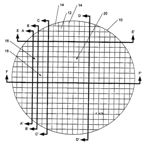
of the present invention. As, seen in Figure 1, a wafer 10, such as a silicon
carbide or
sapphire wafer, has formed thereon a plurality of light emitting devices 12,
such as
light emitting diodes. The periphery of each of the light emitting devices 12
is
defined by a plurality of score lines 14. The score lines 14 may, for example,
be
provided by sawing and/or etching the wafer 10 so as to provide grooves in the
wafer
10 along which the wafer 10 may be separated. For example, with a silicon
carbide
substrate, the score lines may extend into the substrate to a depth which
results in
from about 20,to about 25 pm of the device structure remaining. The light
emitting
devices 12 may have a common light emitting region formed on the wafer 10 or
may
be discrete devices, such as individual devices isolated by mesas, guard
rings,
implanted regions, or the like, formed on and/or in the wafer l0~and~(or in a
layer
formed on the wafer 10.
Alternatively, score lines which, for example, leave about 30 to 40 ~m of the
device structure remaining may be utilized for light extraction which score
lines
which result in from about 20 to about 25 p,m of the device structure
remaining
utilized where the wafer is to be broken. Such may be accomplished by, for
example,
selecting the relatively contiguous devices and determining where the device
array
boundaries are located. Such a determination could then be used to change the
cut
height of the saw forming the score lines. By altering the thickness for score
lines
along a break and score lines provided to differentiate devices and for light
output, the
likelihood of inadvertently breaking the wafer along an incorrect score line
may be
reduced.
According to embodiments of the present invention, the wafer 10 is selectively
separated along score lines 14, which are selected so as to provide a unitized
subset of
4
CA 02473722 2004-07-15
WO 03/065457 PCT/US02/33315
light emitting devices 12. Thus, for example, the wafer 10 may be broken along
score
lines A-A', B-B', E-E' and F-F' to provide a unitized subset 16 of the light
emitting
devices 12 that provides a linear array of 8 light emitting devices.
Similarly, the
wafer 10 may be broken along score lines B-B', C-C', E-E' and F-F' to provide
a
unitized subset 18 of the light emitting devices 12 that provides a 2X8
rectangular
array of light emitting devices. As is fiu~ther illustrated in Figure 1, the
wafer 10 may
be broken along score lines C-C', D-D', E-E' and F-F' to provide a unitized
subset 20
of the light emitting devices 12 that provides an 8X8 square array of light
emitting
devices.
While the light emitting devices 12 in Figure 1 are illustrated as
substantially
square in shape, other shapes of light emitting devices may be provided by
rearranging and/or adding score lines 14. For example, triangular light,
emitting
diodes may be provided by fiuther scoring the wafer 10 to further divide the
light
emitting devices 12. Similarly, combinations of different shaped light
emitting diodes
may also be provided by rearranging and/or adding score lines 14. Thus, for
example,
rectangular and triangular devices may be provided in a single wafer.
Similarly,
different polygonal devices may also be provided in a single wafer.
Additionally,
different shapes, such as arcs, curves or the like may be provided by the
score lines
such that any resulting shape may be provided by separation along selected
score
lines. However, the particular technique of separation may limit the
practicality of
certain shapes. The particular type and/or combination of typesao~.devices in
a
unitized subset of the devices may then be determined by the selection of the
score
lines along which the wafer 10 is broken.
The selective breaking or not breaking of wafer 10 along the score lines of
the
wafer 10 which define the light emitting diodes may be utilized with many
different
types of light emitting devices. Embodiments of the present invention may be
particularly well suited for use with the light emitting diodes described in
United
States Patent Application Serial No. (Attorney Docket No. 5308-162),
entitled "LIGHT EMITTING DIODES INCLUDING SUBSTRATE
MODIFICATIONS FOR LIGHT EXTRACTION AND MANUFACTURING
METHODS THEREFOR" filed January 25, 2002, the disclosure of which is
incorporated herein by reference as if set forth fully herein.
Figure 2 illustrates an interconnection of a unitized subset of light emitting
diodes according to embodiments of the present invention. The unitized subset
of
5
CA 02473722 2004-07-15
WO 03/065457 PCT/US02/33315
light emitting diodes 40 include a substrate 50 having a light emitting region
52
formed thereon. The light emitting diodes 42, 44, 46 and 48 of the unitized
subset of
light emitting diodes 40 may have the ATON shape illustrated in Figure 2,
which
may be provided by the score lines, or may have other shapes or combinations
of
shapes. A conducting material 54 on a support substrate 60 provides electrical
contact
to a contact region and/or regions of the unitized subset of light emitting
diodes 40.
The conducting material 54 may be solder, a eutectic bond and/or conductive
epoxy.
The support substrate 60 has a conducting region 58 thereon, such as a
metallic land
and/or bus, to which a second contact and/or contacts of the unitized subset
of light
emitting diodes 40 is electrically connected by the conductor 56.
The conductor 56 maybe connected to the unitized subset of light emitting
diodes 40 by solder. However, other conductive connections may also be
provided,
such as a eutectic bond and/or conductive epoxy. Furthermore, the light
emitting
diodes 42, 44, 46 and 48 in the unitized subset of light emitting diodes 40
may be
individually connected to the conducting region 84 (e.g. as illustrated in
Figure 3) or
may be daisy-chained together by the conductor 56 and then connected to the
conducting region 58 (e.g. as illustrated in Figure 2). Combinations of daisy-
chained
contacts and individual connections to the conducting region 58, 84 may also
be
provided.
While the embodiments of the present invention illustrated in Figure 2 are
described with reference to a "flip-chip" configuration, where ligl~~
extracted
through the substrate 50, and with reference to light emitting diodes having
contacts
on opposite sides of the device, as will be appreciated by those of skill in
the art in
light of the present disclosure, other configurations may also be utilized
while .still
benefiting from the teachings of the present invention. For example, devices
with
both contacts on the same side of the device may be utilized. Furthermore,
devices
which are not of the "flip-chip" configuration may also be utilized.
Additionally,
while Figure 2 illustrates the unitized subset of light emitting diodes being
mounted
on a support substrate 60, such a support substrate may be omitted.
Turning to Figure 3, a top view of an interconnection of a 2X4 unitized subset
of light emitting diodes 82 is illustrated. As seen in Figure 3, the unitized
subset of
light emitting diodes 82 is mounted on a support substrate 80. Contacts of the
light
emitting diodes of the unitized subset of light emitting diodes 82 are
connected to the
conducting regions 84 of the support substrate 80 so as to provide electrical
6
CA 02473722 2004-07-15
WO 03/065457 PCT/US02/33315
connection to the light emitting diodes. The second contact of the light
emitting
diodes may be made to the opposite side of the light emitting diodes and may
be made
directly to the support substrate 80 by, for example, a soldering process.
While the contacts of the light emitting diodes are illustrated as on opposite
faces of the light emitting diodes in Figure 3, both contacts on a common face
of the
light emitting diodes may also be provided. In such a case, direct electrical
connections from the support substrate 80 may be provided by, for example,
selective
solder connections, eutectic bonds and/or conductive epoxy. Alternatively,
conductors could be connected to both contacts if the contacts were on a face
of the
light emitting diodes opposite the support substrate 80.
Figure 4 illustrates operations according to embodiments of the present
invention. As seen in Figure 4, a wafer with a light emitting region and/or
regions is
fabricated (block 100). The wafer is then scored to define discrete light
emitting
diodes (block 110). This scoring process may produce any desired shape to the
periphery of the light emitting diodes and may be carried out,. for example,
by sawing
and/or etching the wafer to provide the score lines. The scoring of the wafer
is
sufficiently. deep so as to allow the wafer to be broken along the score
lines. The
wafer is then broken along selected ones of the score lines to provide a
unitized subset
of the light emitting diodes having two or more diodes contained therein
(block 120).
The selected score lines may be selected based on one or more criteria. For
example, the score lines may be selected to provide a desired nt~a~nbex of
diodes in the
unitized subset of light emitting diodes.. The score lines may also be
selected to
provide a unitized subset of diodes having a desired optical and/or electrical
property
or properties. For example, the score lines could be selected to provide
diodes with a
desired light output level, wavelength and/or wavelengths. The score lines may
also
be selected to provide a desired wavelength profile, such as a range of
wavelengths.
Similarly, the score lines could be selected to provide a unitized subset of
light
emitting diodes with a desired electrical characteristic, such as forward bias
voltage
Vf. Such a selection may be made based on actual measurements of the light
emitting
diodes on the wafer or may be made based on predicted characteristics of the
light
emitting diodes. Similarly, light emitting diodes within a wafer may be
designed to
have differing characteristics, such as output wavelength. In such a case, the
score
lines could be selected to provide a desired combination of light emitting
diodes
having the differing characteristics.
7
CA 02473722 2004-07-15
WO 03/065457 PCT/US02/33315
After breaking the wafer to provide the unitized subset of light emitting
diodes, connections are made to the light emitting diodes of the unitized
subset of
light emitting diodes (block 130j. Preferably, such connections are made using
solder
technology, however,, eutectic bonds and/or conductive epoxy may also be used.
Furthermore, preferably, the light emitting diodes have connections on
opposite faces
of a substrate and are utilized in a "flip-chip" configuration with light
extracted
through the substrate. In such embodiments, a silicon carbide substrate is
preferred.
While embodiments of the present invention have primarily been described
herein as being separated into unitized subsets of light emitting diodes
through
breaking, as will be appreciated by those of skill in the art in light of the
present
disclosure, other methods for separating the subset of light emitting devices
may be
utilized. For example, the subsets may be separated by sawing, laser cutting,
water jet
milling or other such techniques conventionally utilized for singulation of
individual
dies.
Similarly, while embodiments of the present invention have primarily been
described with reference to each of the light emitting diodes in the unitized
subset of
light emitting diodes having electrical connections provided thereto, the
present
invention should not be construed as limited to such embodiments.. In other
embodiments of the present invention, selected ones of light emitting diodes
of the
unitized subset, which may be all or less than all of the light emitting
diodes, may be
have connections provided. As described above, the light emittan~diodes having
connections provided may be selected to provide a particular characteristic,
such as
wavelength or range of wavelengths, voltage characteristic and/or output level
or the
like. Such selected light emitting diodes may have connections provided as
described
above. Such a selective interconnection may be provided, for example, as
described
in commonly assigned United States Patent Application Serial No. 09/981,523,
entitled "LARGE AREA SILICON CARBIDE DEVICES AND
MANUFACTURING METHODS THEREFOR" which was filed October 17, 2001,
the disclosure of which is incorporated herein by reference as if set forth
fully herein.
In the drawings and specification, there have been disclosed typical preferred
embodiments of the invention and, although specific terms are employed, they
are
used in a generic and descriptive sense only and not for purposes of
limitation, the
scope of the invention being set forth in the following claims.
8