Note: Descriptions are shown in the official language in which they were submitted.
CA 02473836 2004-07-21
WO 03/068669 PCT/SE03/00252
Deflectable microstructure and method of manufacturirig-the~
same through bonding of wafers
Technical field
The present invention relates generally to processes for the manufacture of
free-
hanging micro structures, in particular such structures as mirrors for use in
Spatial Light Modulation (SLM) devices, by employing mirror arrays.
In particular it relates to novel processes for the manufacture of mirror
structures
suitable i.a, for SLM.
Background of the invention
Spatial light modulators (SLM) are transducers that modulate incident light in
a
spatial pattern corresponding to an electrical or optical input. The incident
light
may be modulated in its phase, intensity, polarization, or direction, and the
light
modulation may achieved by a variety of materials exhibiting various
electrooptic or
magnetoopotic effects and by materials that modulate light by surface
deformation.
SLMs have found numerous applications in the areas of optical information
processing, projection displays, and electrostatic printing. See references
cited in L.
Hornbeck, 128 X 128 Deformable Mirror Device, 30 IEEE Trap. Elec. Dev. 539
(1983).
The known beam SLMs have problems including beam insulator charging effects,
lack of overvoltage protection against beam collapse, small-angle and
nonuniform
beam deflection leading to optical inefficiency and nonuniformity, and high
voltage
addressing of the pixels.
US-6,062,461 discloses a manufacturing method, and is incorporated herein by
reference.
Within the semiconductor industry, there are numerous applications that
require
bonding two or more semiconductor wafers together, an example being
CA 02473836 2004-07-21
WO 03/068669 PCT/SE03/00252
2
semiconductor sensors formed by a silicon wafer (referred to herein as a
device
wafer) with a micromachined structure or micromachine, which is capped by a
second wafer (referred to herein as a capping wafer). Specific examples of
semiconductor sensors include yaw (angular rate) sensors, accelerometers and
pressure sensors, each of which typically entails a cavity formed in the
capping
wafer to receive and/or provide clearance for the micromachine of the device
wafer.
Absolute pressure sensors require that the cavity be evacuated and
hermetically
sealed, while the performance of yaw sensors and accelerometers with
resonating
and tunneling micromachines generally benefit if the cavity is evacuated so
that the
micromachine operates in a vacuum.
The integrity of the bond between the wafers is essential for promoting the
life of a
semiconductor sensing device. As a result, various bonding techniques have
been
suggested for the purpose of maximizing the strength and reliability of the
bond.
For example, the use of adhesives, dielectrics such as glass frit, and solders
as
intermediate bonding materials have all been suggested in the prior art.
Silicon
direct and anodic bonding techniques that do not require an intermediate
material
have also been used. As can be expected, each of these bonding techniques can
be
incompatible or less than ideal for certain applications. An example of
particular
interest here is the manufacture of resonating and tunneling micromachines
that
require a vacuum for improved performance. Silicon direct and anodic bonding
methods require very smooth bonding surfaces, and therefore cannot produce a
vacuum seal when unplanarized metal crossunders are employed, as is often
required to electrically interconnect resonating and tunneling micromachines
to
bond pads outside the vacuum-sealed cavity of a sensor. In contrast, organic
adhesives, glass frit and solder can be used to cover metal steps of up to
21,000
.ANG. found on CMOS, bipolar and BICMOS wafers. However, organic adhesives
have not been found to reliably seal micromachines under vacuum, and bonding
techniques employing glass frit require temperatures typically in the range of
about
385~C. to 410~C., which can cause polysilicon, electroformed metal and LIGA
micromachines to warp, bend and/or become electrically unstable. As a further
example, yaw sensors with resonating micromachined structures are prone to
exhibit zero offset drift, compass effect and start-up drift if subjected to
the
CA 02473836 2004-07-21
WO 03/068669 PCT/SE03/00252
3
temperatures necessary to bond wafers with glass frit.
In contrast, solder wafer bonds can be formed at temperatures of 350~C. and
less,
and have been successfully used to form vacuum seals between wafers having a
micromachined structure, as disclosed in U.S. patent application Ser. No.
08/785,683 to Sparks et al., assigned to the assignee of the present
invention.
Because solder alloys cannot wet or bond to semiconductor materials such as
silicon and ceramics, solder wafer bonding requires solderable bond pads
adhered
to each wafer and to which the solder will metallurgically bond. As shown in
Sparks
et al., solder bonding of two wafers to form an evacuated cavity requires a
pair of
complementary solderable rings on the device and capping wafers. A drawback to
this requirement is the close alignment tolerances required to align the
solderable
rings, which complicates the bonding process when performed in a vacuum to
obtain an evacuated cavity for housing the micromachine.
From the above, it can be appreciated that improved bonding processes are
desired
to form a semiconductor sensor having a micromachined structure enclosed in an
evacuated cavity and metal crossunders interconnecting the micromachine to
bond
pads outside of the cavity.
US-5,061,049 discloses a device that overcomes some of the problems associated
with the prior art technology. However, there are still some problems, i.a.
the Al
mirrors are made by deposition processes and are not mono crystalline, and
therefore they cannot be perfectly planar, neither on a microscale nor on a
macroscale. Polishing will always introduce some surface roughness. Also, the
prior
art devices are "binary" in their nature, i.e. they are either "on" or "off'
(deflected or
non-deflected). Furthermore, they all suffer from hysteresis effects to some
extent.
Finally, the usable wave lengths are restricted to the visible spectrum.
Summary of the invention
Thus, there is still room for improvements in the f°ield of devices
comprising free-
hanging micro structures, such as micro mirrors for SLM, and it is the object
of the
CA 02473836 2004-07-21
WO 03/068669 PCT/SE03/00252
4
present invention to provide a novel method for making such free-hanging
devices
in general, and in particular mirrors and/or arrays, that have superior
properties
compared to previously known devices. This object is achieved in one aspect
with a
method according to claim 1.
In one embodiment the method involves the use of eutectic solder material for
the
bonding of wafers to form well defined structures exhibiting well defined
spacing
between wafers.
In another embodiment the spacing accuracy is further improved by employing
spacing elements.
In a further embodiment the bonding is achieved by utilizing the material in
one of
the wafers as one component of the eutectic bond.
Further embodiments are defined in additional dependent claims.
In a further aspect, the invention comprises mono-crystalline free-hanging
members, e.g. mirrors, preferably made of silicon or other materials that can
be
processed in a single crystalline state to form micro structures.
The advantages with the novel and inventive method is the ability to
manufacture
devices exhibiting i.a.
- superior mechanical properties (no hysteresis effects);
- perfectly planar reflective surface, both with regard to surface roughness
and
macroscopic planarity (no curving of the surface);
- excellent reflective properties, operable with wave lengths down to about
100
nm (deposition of different materials, e.g metals such as gold increases the
reflectivity for longer wave lengths 600-2000nm) ;
- sufficiently intrinsically electrically conductive (doping can be provided
during manufacture) .
Brief Description of the Drawings
CA 02473836 2004-07-21
WO 03/068669 PCT/SE03/00252
The invention will be described in detail below with reference to the
drawings, in
which
5 Fig. 1 shows two wafers to be bonded together;
Fig. 2 shows the wafers bonded together;
Fig. 3 shows an assembly where mirrors have been created by etching
sacrifical material;
Fig. 4 shows two non-bonded wafers according to an alternative
embodiment;
Fig. 5 shows the embodiment of Fig. 4 in a finished state.
Fig. 6 shows two wafers before bonding according to a further
embodiment;
Fig. 7 shows the wafers in Fig. 6 bonded together;
Fig. 8 shhows a finished structure;
Fig. 9 is a perspective view of a further embodiment of the invention with
two non-bonded wafers;
Fig. 10 shows the cross-sectional view A-A~ in Fig.9;
Fig. 11 shows the two wafers of the embodiment of Figs. 9-10 before
bonding the wafers together;
Fig. 12 shows the embodiment of Fig. 9-10 with the wafers bonded
together using an eutectic bond;
CA 02473836 2004-07-21
WO 03/068669 PCT/SE03/00252
6
Fig. 13 shows the dicing of the bottom wafer, the top wafer is used as a
carrier/support wafer;
S Fig.14 shows an assembly where a te~x~,porary carrier wafer is used, and
wherein the top wafer has 'been sacrificially removed;
Fig.15 shows an assembly where reflecting mirrors have been created by
metal deposition and the suspension and hinges as well as the device
itself (e.g, dicing tracks) are defined by etching according to a third
embodiment; and
Fig. 16 shows the final diced mirror device released from the temporary
carne- wafer according to a third embodiment,
Detailed desariptioa of the iaventioa
For the purpose of the present invention, the terms "eutectic wafer bonding",
"eutectic wafer bond", eutectic bump" and solder bump", will have the meanings
ZO explained below.
Some alloys of metals and semiconductor materials form. eutectic compositions
that
solidifies/freeaes at lower temperatures than all other compositions formed by
the
materials in question. This effect can. be used for~o:irr.in.g or bonding two
different
materials together.
A "eutectic bond", is formed when two materials capable of forming a eutectic
are
bro~xght together iz~ a non-oxidizing exwironment (vender inert gas or .ix~.
vacuum)
while applying heat (and optionall~r pressure) so as to heat the materials to
a
temperature above the eutectic point_
If two wafers (e.g. of singXe crysta77ine silicon) on the surfaces of which
two or more
eutectic materials are present are forced together under pressure and with
heat
CA 02473836 2004-07-21
WO 03/068669 PCT/SE03/00252
7
applied, the two materials will form a "eutectic wafer bond". The simplest
case is
when one eutectic material is provided on a respective wafer. However, a
number of
other combinations are possible.
Preferred materials for forming eutectic bonds, for the purpose of the present
invention, are Au and Si. Thereby, the silicon is provided as the wafer
material, and
suitably pure silicon wafers are used. Alternatively, wafers of other
materials with
deposited silicon on the surface can be used. The Au is provided on selected
areas
or spots, on one or both of the wafers that are to be joined together by
bonding (for
the purpose of the present invention these areas or spots are referred to as
"eutectic
bumps", although they consist of a single material and do not form a eutectic
alloy
until bonding has occurred). However, many other eutectic alloys are known in
the
art.
The eutectic point of the preferred eutectic bonding of Au-Si is at a
temperature of
363°C. When two (silicon) wafers having the suitable Au bumps are
heated to this
temperature a liquid Au-Si alloy that contains 3% Si and 97% Au is formed. The
actual bonding temperature is some tens of degrees higher than the actual
eutectic
point, which allows sufficient solid-liquid inter-diffusion at the interface.
Optionally
also a pressure can be used during the bonding, generating the necessary
temperature increase to form the eutectic composition. The eutectic alloy then
solidifies on cooling and the wafers are thereby bonded together.
The generic term "eutectic bonding", as defined herein, includes the notion of
"solder bonding", where two or more materials are deposited on at least one of
the
wafers which should be bonded together. Commonly used materials, referred to
as
"solder alloys", include AuSn, PbSn, AgSn, InSn, SbSn. For the purpose of the
present invention the preferred alloy is AuSn. Several ways of depositing and
structuring these solder alloys are known in art. A solder or "solder bump" or
"eutectic bump" is formed when these alloys are heated to the eutectic point
forming, so called re-flow. This commonly used definition of a solder is
extended for
the purpose of the present invention in the same way as for eutectic bumps.
This
means that also configurations where one of the materials, e.g. Au could be
CA 02473836 2004-07-21
WO 03/068669 PCT/SE03/00252
8
structured on one wafer in solder or eutectic bumps, and then the other
material
needed to form the eutectic solder, are structured on the other wafer in the
same
bump configuration, are referred to as "eutectic bumps". This type of bonding
is
also included in our definition of a solder bonding even though it may differ
from
the common notion of a solder. The other wafer to be solder bonded will
require a
soldering area of a material that will wet the solder when they are brought
into
contact and heated to and above the melting point (=eutectic point) of the
solder.
The nomenclature "AuSn" or "AuSi" refers to a mixture (=alloy) of Au and Sn,
and
Au and Si, respectively. The Au and Sn can be deposited as separate layers
with the
understanding that the Sn will tend to migrate at elevated temperature into
the ,Au
to form the eutectic solder bumps. However, for ease of manufacturing, the
Au/Sn
eutectic is preferably deposited as separate layers except in those
embodiments
where the migration of Sn into Au or Au into Si is specifically relied upon to
form
eutectic AuSn solder (e.g by a re-flow process), AuSi eutectica, respectively.
One of the important features of the invention is the provision of hinge
members for
the micro structures, e.g. mirrors, such that the structures are deflectable
from a
nominal position. The deflection is achieved by electrostatic action through
application of voltage across a gap between an electrode (on the bottom wafer)
and
the structure, e.g. the mirror. The hinge must be defined so as to have a
lateral
extension or width that is small compared to the width of the structure that
is to be
deflectable. Preferably, the hinge should have a point of attachment or
connection
to the deflectable member that is located about the mid point of one edge of
said
member. In the case of circular structures, or other irregular shapes, the
lateral
extension of the hinge should be such that a sufficient flexibility is
achieved for the
electrostatic action to enable said deflection. The actual ratio between the
width or
extension of the hinge will be a matter of experimentation, that can be
performed by
the skilled man without undue burden.
The hinges can be achieved in different manners. The basic feature is that a
hinge
should be thin enough that deflection is easily achieved. If the deflectable
structure
in itself is sufficiently thin, it will suffice to make the lateral extension
of the hinge
CA 02473836 2004-07-21
WO 03/068669 PCT/SE03/00252
9
small enough compared to the width of the structure. If on the other hand the
structure is so thick that it renders the structure itself too rigid, the
hinge can be
made to be thinner, by partially etching through the material at the hinge,
such
that the part of the structure that is free hanging and the part that is
attached to
the support is thicker than the hinge member. The hinges can also be defined
by
making the length of the hinge from the point of attachment on the free
hanging,
deflectable micro structure, to the point of attachment to its support
structure,
sufficiently large to render the micro structure deflectable.
In one embodiment there are at least two hinges forming a gimbal structure, so
as
to render the micro structure deflectable in two directions.
Figs. 1 - 5 schematically shows an embodiment of the process according to the
invention of assembling two wafers for the purpose of making mirror arrays.
The process comprises making two separate wafers, a first wafer (upper wafer
in
Fig. 1) carrying the mono/single crystalline materials, e.g. silicon, GaAs,
SiC etc,
from which the mirrors are to be made, and a second wafer carrying CMOS
electronics, electrodes, bond pads and other components necessary for the
function
of the final array.
In summary the process can be described as follows:
Making the SOI-wafer (Top-wafer), Fig. 1:
1. - Evaporation Ti/Au for plating base (eg. 1001/ 10000 to cover entire wafer
2. - Lithography and Electroplating solder material, Au/Sn (e.g.l llm) in
finite
bumps and in separate layers
3. - Lithography and Au/Ti etch
Making the CMOS or bottom electrode wafer, Fig. 1:
CA 02473836 2004-07-21
WO 03/068669 PCT/SE03/00252
1. - Evaporation (or electroplating (Au), electroless plating (Ni/Au) or
sputtering
(TiW/Au) a solderable layer (e.g. 100A/ 100010
2. - Lithography and etch of this solderable layer
5 Bonding of wafers
1. - Wafer bonding (heat to 300~C and pressure e.g 0.5 bar)
2. - Stripping the thick sacrificial layer of the SOI-wafer (Deep Reactive Ion
etch)
and a wet HF-etch of oxide layer
10 3. - Lithography and silicon etch to define the mirrors with hinges
Thus, the first wafer (top wafer in Fig. 1) can be a conventional SOI wafer
(Silicon
On Insulator), commonly used in the semiconductor industry as starting
material in
numerous applications. However, it is not strictly necessary to employ an SOI,
since
other etch stop layers are possible. The SOI wafer can be provided with a
pattern of
A1 in thin layers, deposited by e.g. sputtering and defining the final
mirrors.
However, the provision of A1 is not required for the purpose of the invention,
and
can be dispensed with. For certain applications the single crystalline silicon
itself
will have a sufficient reflectivity and conductivity to function as mirror/
electrode
material. If its conductivity must be increased, the silicon wafer can be
doped in
selected regions according to a desired pattern so as to define the mirrors.
In such
cases the final mirror elements are produced by masking/etching after bonding
the
wafers together to form an assembly, as will be described further below.
Solder bumps of the selected solder material (Au/Sn shown) are plated onto the
wafer at the desired points, e.g. in at least one point near an edge of the
area
defining the mirror (see Fig. 1), so as to render the final mirror "beam"
cantilevering.
The number of bumps may vary depending on the shape of the beam.
The second wafer (bottom wafer in Fig. 1), which can be a CMOS wafer or a
plain Si
wafer structured or non-structured, comprises electrodes made by depositing
suitable electrically conductive materials such as Al, Au, Ni, Ti etc or using
highly
doped silicon as it is or using a plain or structured wafer with wafer through
vias.
CA 02473836 2004-07-21
WO 03/068669 PCT/SE03/00252
11
There are also provided soldering bumps of e.g. Ni/Au, which is a preferred
material, but in no way the only possible. These bumps are disposed in a
pattern
exactly matching the solder bumps on the first wafer. They are made by
electroplating or by electroless plating.
The wafer is suitably partially covered by a thin oxide layer, or a layer of
some other
non-wetting material, such that the electrodes as well as the Ni/Au bumps are
exposed for the purpose of creating different wetting properties on the bumps
and
the area surrounding them. Also the upper wafer should be provided with non-
wetting material surrounding the contact spots with which the solder is to
cooperate to form the final bond.
For assembly the two wafers are brought together (Fig. 2) in a non-oxidizing
environment (under inert gas or in vacuum) while applying heat (and optionally
pressure) so as to melt the solder. When the wafers are aligned, heating is
terminated and the solder solidifies.
When the wafers have been bonded together yielding the structure seen in Fig.
2,
the sacrificial layer on the SOI is etched away (wet or dry), and then the
oxide is
etched away, by dry plasma etc or wet etch, the latter in order to maintain
the
mirror surface finish.
The silicon layer is patterned by lithographic methods and etched to create
the
desired beam structure for the mirrors.
Optionally A1 is deposited (see Fig. 3) by sputtering, and the definition of
the final
structures is made by suitable patterning and etching in conventional way.
Finally, the individual chips are self aligned. This is an important feature
of the
invention and is performed by making use of the fact that the solder has other
wetting properties on the Ni/Au bumps than on the surrounding oxide layer. The
self alignment is achieved by cutting out the individual mirror array chips
from the
CA 02473836 2004-07-21
WO 03/068669 PCT/SE03/00252
12
wafer assembly, and exposing each of them separately to heat again so as to
melt
the solder. Thereby the solder will float out to completely cover the Ni/Au
bumps,
and if there should have occurred a slight misalignment in the wafer bonding
process, the two parts of each mirror chip will adjust themselves by this
operation.
Another important and advantageous feature of the present invention is that if
the
Ni/Au bumps are made to exhibit a larger surface area than the matching solder
bumps, it will become possible to reduce the spacing between the wafers in the
bonding process. Namely, the solder bump, which has a defined height as
provided
on the upper wafer, will float out on the larger Ni/Au bump, and in the
process the
height of the Au/Sn bump is of course reduced. This enables a reduced spacing
between wafers than what otherwise would be possible, and thus the final
mirror
can be located closer to the electrode, and with a higher accuracy.
Fig. 4 illustrates a further feature of the invention, namely the provision of
spacer
members defining the distance between mirror and electrode. These spacers are
provided on the SOI wafer (first wafer) in alignment with the contact bumps
(Ni/Au)
on the CMOS wafer (second wafer) and on which there has been provided solder,
e.g. Au/Sn. When the wafers are brought together and the heat is applied, the
solder melts and spacer members will come into contact with the CMOS wafer,
thereby providing an exact definition of the spacing between the wafers, which
can
be seen in Fig. 5. This corresponds to the arrangement in Fig. 3, wherein the
solder
itself will define the spacing.
EMBODIMENT 3
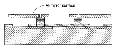
Fig. 8 schematically shows a third preferred embodiment of the final mirror or
mirror arrays device fabricated according to the invention. ,
In summary the process can be described as follows with reference to Figs. 6-
7:
Making the SOI-wafer (Top-wafer) which is then normally is not processed
further
before the AuSi eutectic bonding. Optionally this wafer can be deposited with
a
CA 02473836 2004-07-21
WO 03/068669 PCT/SE03/00252
13
metal layer as mirror electrodes following the processing according to
embodiment
1.
The second wafer (bottom wafer in Fig. 6), which can be a CMOS wafer or a
plain Si
wafer structured or non-structured, comprises electrodes made by depositing
suitable electrically conductive materials such as Al, Au, Ni, Ti etc or using
highly
doped silicon as it is or using a plain or structured wafer with wafer through
vices
(i.e. electrical connections through the wafer). The bottom wafer is also
provided
with eutectic bumps (as defined above) of e.g. Ni/Au or TiW/Au, consisting of
a
diffusion barrier and a top layer of gold. Other eutectic alloys suitable for
bonding
exists and are known to the skilled man, but our preferred materials are Au
bumps
bonding to Si, although this is in no way the only possible material. These
bumps
are disposed in a pattern but must not match any bumps on the first wafer, as
in
the case for the previously described embodiment. The bumps are made by
electroplating, by electro less plating, by evaporation or by sputtering or a
combination of these methods.
For assembly the two wafers are brought together in a non-oxidizing
environment
(under inert gas or in vacuum) without any need for coarse alignment as with
the
process according to embodiments described above (Figs. 1-5). This is an
important
feature of the invention and is performed by making use of the fact that the
Au
bumps could be directly bonded to the Silicon without any metal layers needing
the
good wetting property. Ap plying heat (and optionally pressure) the eutectic
phase of
the alloy is obtained. At the eutectic point (e.g. at 363°C for the
AuSi alloy), a liquid
Au-Si alloy that contains 3% Si and 97% Au is formed. The actual bonding
temperature is some tens of °C higher than the eutectic point, which
allows
sufficient solid-liquid interdiffusion at the interface. The eutectic alloy
then
solidifies on cooling and the wafers are bonded together. In case a metal
electrode is
used a coarse alignment of the two wafers are needed before the bonding (e.g.
the
electrodes on respective wafer need to overlap with each other). When the
wafers are
aligned, heating is terminated and the eutectic bumps solidifies.
CA 02473836 2004-07-21
WO 03/068669 PCT/SE03/00252
14
When the wafers have been bonded together yielding the structure seen in Fig.
7,
the sacrificial layer on the SOI is etched away (wet or dry), and then the
oxide is
etched away, following the process described above for the previously
described
embodiment.
The silicon layer is patterned by lithographic methods aligning the mask
direct
against the patterns (e.g. electrodes or eutectic bumps) on the second wafer
(bottom
wafer) and etched to create the desired beam/hinge structure for the mirrors.
This
is an important feature of the invention since it makes use of direct
alignment of
the mask towards patterns on the wafer (e.g. the conventional method in
semiconductor / IC / MEMS manufacturing) rather than relying on the alignment
accuracy during bonding. Using the above described feature of direct alignment
the
mis-alignment compensation techniques of the bonding, by self alignment
feature,
used in the previously described embodiments are not needed. The final SLM
device
is shown in Fig. 8.
Optionally A1 is deposited by sputtering, and the definition of the final
structures is
made by suitable patterning and etching in conventional way.
EMBODIMENT 4
Fig. 9 schematically shows a perspective view of a fourth embodiment of the
final
mirror or mirror arrays device fabricated according to the invention. For
clarity the
mirrors and hinge/suspension structures are removed in the right part of the
drawing looking into the cavity where the electrodes are shown. Fig. 10 is a
cross
section at
A-A' in Fig. 9.
The process comprises making two separate wafers, a first wafer carrying the
3 0 mono / single crystalline materials, e. g. silicon, GaAs, SiC etc, from
which the
mirrors) are to be made, and a second wafer carrying components necessary for
the
function of the final mirror device such as electrodes, bond pads, via
contacts,
CA 02473836 2004-07-21
WO 03/068669 PCT/SE03/00252
CMOS electronics. Then the two wafers are bonded together using an eutectic
bonding method according to the present invention.
In summary the process can be described as follows:
5
Making the SOI-wafer (Top-wafer, Fig. 11):
1. - Evaporation or sputtering of thin layers of Ti/Au as electrode
structures.
Also the eutectic bumps used for bonding spots are defined in this step.
10 2. - Lithography and Si etch (preferably dry plasma DRI-etching) forming
hinge
structures. (not necessary)
Making the bottom electrode wafer (Fig. 11):
15 3. -Etching of cavities (not necessary), oxidation, (opening of contact
holes for
grounding the substrate), Metal deposition of a seed-layer.
4. - Lithography (lift-off or plating mold) and deposition of an eutectic
structure
(Au/Sn as an example of solder or only Au as an eutectic sublayer) by
evaporation, sputtering or electroplating (thickness 0.5-10 I_lm),
5. - Lithography and etch of the seed-layer used to define the electrode
patterns
Bonding of wafers (Fig. 12):
6. - Wafer bonding (heat above 363C and pressure e.g 0.5 bar for eutectic
bonding with Au bumps direct to Si or heat above 283C for AuSn - Au solder
bonding)
7. - Lithography and etch of oxide and silicon to define die tracks from
backside
on bottom wafer to define and later separate each component, the top wafer
is used as a robust carrier wafer
8. - Mounting to a temporary carrier wafer using resolvable tapes or other
adhesives such as resist
9. - Stripping the thick layer of the SOI-wafer (Deep Reactive Ion etch) and a
wet HF-etch of oxide layer
CA 02473836 2004-07-21
WO 03/068669 PCT/SE03/00252
16
10.- Metal deposition, lithography and metal etch to define the reflective
part of
the mirrors
11.- Lithography and silicon etch to define the mirrors with hinges as well as
die
tracks.
12.- Removal from the temporary carrier wafer (e.g. release of the adhesive
material either by heating the wafer for removal of the tape or solvent
cleaning to remove the resist) then final individual mirror devices according
to this invention are finished.
Thus, the first wafer (top wafer in Fig. 11) can be a conventional SOI wafer
(Silicon
On Insulator), commonly used in the semiconductor industry as starting
material in
numerous applications. However, it is not strictly necessary to employ an SOI,
since
other etch stop layers are possible. The SOI wafer can be provided with a
pattern of
a thin metal layer, deposited by e.g. sputtering or evaporation and defining
the final
mirror electrodes as well as the eutectic bumps defining the bonding areas
later on.
However, the provision of the metal layer is not required for the purpose of
the
invention, and can be dispensed with. For certain applications the single
crystalline
silicon itself will have a sufficient reflectivity and conductivity to
function as
mirror/electrode material. If the conductivity must be increased, the silicon
wafer
can be doped in selected regions according to a desired pattern so as to
define the
mirror electrodes. In such cases the final mirror elements are produced by
masking/etching after bonding the wafers together to form an assembly, as
described above. For certain eutectic bonding alloys (e.g. Au-Si) the top
whole single
crystalline surface is used as the bonding areas. Then no eutectic bumps are
needed. To minimize any bimorph effects coming from unsymmetrical mirrors
which could create mirror curvature the same material and thickness should be
used both for electrodes and later on as the reflective material on the other
side of
the mirror. Therefore the choice of material is dependent on which wavelengths
the
mirror should reflect. For some applications the electrode material isn't
suitable as
eutectic bumps then the deposition and photolithography patterning of the
electrodes and the eutectic bumps have to be made in two separate steps.
CA 02473836 2004-07-21
WO 03/068669 PCT/SE03/00252
17
Optionally the top wafer could be photolithography patterned and silicon
etched to
a certain depth into the SOI wafer to form optimum hinges, gimbals and
suspension
springs, via structures (partially through) or other structures. Including
this etching
step the mirrors remain thicker, e.g. exhibiting less curvature, while the
become
softer and thus easier to actuate.
When solder bonding should be used the top wafer is suitably partially covered
by a
thin oxide layer, or a layer of some other non-wetting material, such that the
electrodes as well as the Ni/Au bumps (e.g. bonding spots with which the
solder is
to cooperate to form the final bond) are exposed for the purpose of creating
different
wetting properties on these spots and the area surrounding them. Also the
bottom
wafer should be provided with non-wetting material surrounding the solder
bumps.
The second wafer (bottom wafer in Fig. 11), which can be a structured or non-
structured plain Si wafer or a CMOS wafer or a wafer with wafer-through vies,
comprises electrodes made by depositing suitable electrically conductive
materials
such as Al, Au, Ni, Ti, TiW etc. or doped silicon areas. To increase the
tilting angle
of the mirrors a cavity could be formed under the mirrors) by wet e.g. KOH or
dry
plasma DRI-etching. Then an insulation layer e.g. oxide is needed before the
metallization of the electrodes. By opening up contact holes through this
oxide
grounding the substrate by special grounding electrodes/pads could be achieved
and also the eutectic bumps could be grounded. Then a deposition of a seed-
layer is
performed. Our preferred seed-layer consists of an adhesion layer (e.g. Ti or
Cr) and
a diffusion barrier (e.g. Ni, Pt, TiW) and then a gold layer provided by
evaporation
(or electroplating (Au), or electroless plating (Ni/Au), or sputtering (TiW/Au
or
combination of these with a typical thickness of 100A/ 1000A/4000-10.000 A).
The
final gold layer should to be thick enough for wire bonding. However, other
materials are of course possible
Eutectic bumps of the selected material are deposited onto the bottom wafer at
the
desired points, e.g. on a frame around the mirrors as illustrated in Figs. 9
and 11.
The number of bumps may vary depending on the size of the mirrors. However, it
is
CA 02473836 2004-07-21
WO 03/068669 PCT/SE03/00252
18
not strictly necessary to employ a frame with eutectic bonding materials
between
each mirror, also other attachment/suspension configurations are possible.
Our two preferred eutectic bumps are Ni/Au (for Au-Si eutectic bonding) or
AuSn
(for AuSn-Au solder bonding), but these are in no way the only possible
choices for
eutectic bonding. These bumps are disposed in a pattern exactly matching the
bonding contact areas Ni/Au for solder bonding) on the top wafer but for the
case of
Au-Si eutectic bonding the Au bumps on the bottom wafer don't need to fit with
bumps on the top wafer since the whole wafer consist of bonding areas.
However,
when metallized electrodes are used on the top wafer the two wafers need to be
aligned to each other in a way that the electrodes on respective wafer overlap
with
each other. The bumps on the bottom wafer are preferably made by
electroplating
(Au or Au/Sn) but also electroless plating (Au) or sputtering (Au) or
evaporation (Au
or Au/Sn), screen-printing (AuSn) as well as other metalisation methods can be
used.
For assembly the two wafers are brought together in a non-oxidizing
environment
(under inert gas or in vacuum). Applying heat (and optionally pressure) the
eutectic
phase of the alloy is obtained. At the eutectic points (e.g, at 363°C
for the AuSi alloy
or 282°C for the AuSn alloy), a liquid alloy is formed. The actual
bonding
temperature is some tens of °C higher than the eutectic points, which
allows
sufficient solid-liquid interdiffusion at the interface. The eutectic alloy
then
solidifies on cooling and the wafers are bonded together. When the wafers are
aligned, heating is terminated and the eutectic bumps solidifies and a solid
assembly of the two wafers into one robust wafer package is formed as shown in
Fig. 12.
When the wafers have been bonded together yielding the structure seen in Fig.
l2,
the backside of the bottom wafer is photolithography patterned followed by
oxide
and silicon etching to define die tracks for later separation of the different
dies on
the wafer into individual free dies. The silicon etch (preferable dry DRIE)
stops on
the oxide on the front side of this wafer. The top wafer is used as a robust
carrier
wafer as shown in Fig. 13.
CA 02473836 2004-07-21
WO 03/068669 PCT/SE03/00252
19
The two bonded wafers (one package) is then mounted on a temporary carrier
wafer
using some adhesive materials (resolvable tapes, resist, etc). When the wafers
have
been bonded together and mounted on the temporary carrier wafer yielding the
structure seen in Fig. 14, the sacrificial layer on the SOI is etched away
(wet or dry),
and then the oxide is etched away, by dry plasma etc or wet etch, the latter
in order
to maintain the mirror surface finish.
Optionally a reflective material (preferably the same material, processing
method
and thickness as for the electrode on the other side of the mirror to achieve
a flat
mirror) is deposited by sputtering or evaporation, and the definition of the
final
reflective mirror area is made by suitable patterning and etching in
conventional
way. To minimize the amount of photolithography masks the same mask could be
used for the lithography of the electrodes and solder spots (on bottom side of
the
SOI wafer) as for the reflective mirrors (on the top side of the SOI wafer
after
sacrificial removal of the carrier substrate).
The silicon layer is patterned by lithographic methods and etched to create
the
desired hinge structure for the mirrors as shown in Fig. 15.
Finally, the individual chips are released from the temporary carrier wafer by
release of the adhesion layer. A single finished structure is shown in Fig.
16.
Optionally, the individual chips could be self aligned in the same way as
already
described for embodiment 1. Also the use of larger Ni/Au bumps than the AuSn
solder could be used to reduce the height of the bonding bumps for closer
vertical
distance between the electrode areas in the same way as described above in
embodiment 1.
EMBODIMENT 5:
Similiar structure as embodiment 4 but placing the solder on top wafer and
contact
areas on the bottom wafer (as embodiment 1 but with the final structure
according
to embodiment 4).
CA 02473836 2004-07-21
WO 03/068669 PCT/SE03/00252
EMBODIMENT 6:
Similar structure as embodiment 4 but bonding Silicon rods (epitaxial grown or
defined by etching on bottom wafer) bonding to an Au eutectic bump on the top
5 wafer.
Finally, the individual chips are self aligned. This is an important feature
of the
invention and is performed by making use of the fact that the solder has other
wetting properties on the Ni/Au bumps than on the surrounding oxide layer. The
10 self alignment is achieved by cutting out the individual mirror array chips
from the
wafer assembly, and exposing each of them separately to heat again so as to
melt
the solder. Thereby the solder will float out to completely cover the Ni/Au
bumps,
and if there should have occurred a slight misalignment in the wafer bonding
process, the two parts of each mirror chip will adjust themselves by this
operation.
Another important and advantageous feature of the present invention is that if
the
Ni/Au bumps are made to exhibit a larger surface area than the matching solder
bumps, it will become possible to reduce the spacing between the wafers in the
bonding process. Namely, the solder bump, which has a defined height as
provided
on the upper wafer, will float out on the larger Ni/Au bump, and in the
process the
height of the Au/Sn bump is of course reduced. This enables a reduced spacing
between wafers than what otherwise would be possible, and thus the final
mirror
can be located closer to the electrode, and with a higher accuracy.