Note: Descriptions are shown in the official language in which they were submitted.
CA 02474054 2004-07-22
WO 03/063211 PCT/US03/02115
-1-
APPARATUS INCORPORATING SMALL-FEATURE-SIZE AND LARGE-
FEATURE-SIZE COMPONENTS AND METHOD FOR MAKING SAME
BACKGROUND OF THE INVENTION
Field of the Invention
[001] The field of the invention generally relates to apparatuses
having both large-feature-size components and small-feature-size
components, and methods of making such apparatuses. The invention
more particularly relates to combination of VLSI integrated circuits and
macro-scale components to form a single device.
Description of the Related Art
[002] VLSI provides many effective methods for creation of
microscopic-scale and smaller components. Such miniaturization
provides many advantages in terms of speed of operation, size of
footprint, amount of necessary resources, and speed of manufacture for
electronic devices.
[003] Unfortunately, some components of electronic devices are
not well-suited to formation through well-known VLSI processes.
These components often are necessarily very large (macroscopic-
scale) relative to devices or components of devices formed through
VLSI. One such component is an antenna, which may need to have a
characteristic length to allow for adequate transmission on a preferred
frequency, and for which the characteristic length in question may be
appropriately measured in centimeters or meters for example.
Formation of a conductor for use as an antenna using VLSI tends to
waste time and material resources, as a 30 cm conductor (for example)
can easily be formed through less expensive processes.
CA 02474054 2004-07-22
WO 03/063211 PCT/US03/02115
-2-
[004) Thus, the problem then becomes a matter of combining a
large-scale component such as an antenna with a small-scale
component such as an integrated circuit. For a conventional radio, this
may involve use of packaging for the integrated circuit, conductors on a
printed circuit board, a connector attached to the printed circuit board,
and an antenna attached to the connector. This approach is simple
enough for a device having rigid packaging and flexible size constraints.
However, other applications may have more demanding requirements
for size and materials cost.
(005] In particular, it may be useful to have a small radio-
transmitter with flexible materials allowing for bending and other
abusive actions without degradation in functionality. Similarly, such a
small radio-transmitter may need to be producible rapidly in quantities
of millions or billions, thus requiring ease of assembly and relatively
inexpensive materials on a per-unit basis. Using a printed-circuit board
approach for such a radio-transmitter will likely not succeed. Moreover,
avoiding such time (and/or space) consuming processing operations
as thermal cure may be advantageous.
[006] It is possible to separately produce elements, such as
integrated circuits and then place them where desired on a different
and perhaps larger substrate. Prior techniques can be generally
divided into two types: deterministic methods or random methods.
Deterministic methods, such as pick and place, use a human or robot
arm to pick each element and place it into its corresponding location in
a different substrate. Pick and place methods place devices generally
one at a time, and are generally not applicable to very small or
numerous elements such as those needed for large arrays, such as an
active matrix liquid crystal display. Random placement techniques are
more effective and result in high yields if the elements to be placed
CA 02474054 2004-07-22
WO 03/063211 PCT/US03/02115
-3-
have the right shape. U.S. Patent No. 5,545,291 and U.S. Patent No.
5,904,545 describe methods that use random placement. In this
method, microstructures are assembled onto a different substrate
through fluid transport. This is sometimes referred to as fluidic self
assembly (FSA). Using this technique, various integrated circuits, each
containing a functional component, may be fabricated on one substrate
and then separated from that substrate and assembled onto a
separate substrate through the fluidic self assembly process. The
process involves combining the integrated circuits with a fluid, and
dispensing the fluid and integrated circuits over the surface of a
receiving substrate that has receptor regions (e.g., openings). The
integrated circuits flow in the fluid over the surface and randomly align
onto receptor regions, thereby becoming embedded in the substrate.
[007] Once the integrated circuits have been deposited into the
receptor regions, the remainder of the device can be assembled.
Typically, this involves coating the substrate with a planarization layer to
provide electrical insulation and physical retention for the integrated
circuits. The planarization layer creates a level surface on top of the
substrate by filling in the portions of the receptor regions that are not
filled by integrated circuits. After the planarization layer has been
deposited, other elements, including pixel electrodes and traces for
example, may be installed.
[008] Using FSA, the functional components of the device can
be manufactured and tested separately from the rest of the device.
SUMMARY OF THE INVENTION
[009] The present invention relates generally to the field of
fabricating elements on a substrate. In one embodiment, the invention
is an apparatus. The apparatus includes a substrate having
CA 02474054 2004-07-22
WO 03/063211 PCT/US03/02115
-4-
embedded therein an integrated circuit, the integrated circuit having a
conductive pad. The apparatus further includes a conductive medium
attached to the conductive pad of the integrated circuit. The apparatus
also includes a large-scale component attached to the conductive
medium, the large-scale component electrically coupled to the
integrated circuit.
[010] In an alternate embodiment, the invention is a method.
The method includes attaching a conductive medium to a substrate
having embedded therein an integrated circuit such that the conductive
medium is connected electrically to the integrated circuit. The method
also includes attaching a large-scale component to the conductive
medium such that the large-scale component is electrically connected
to the conductive medium.
[011] In another alternate embodiment, the invention is an
apparatus. The apparatus includes an integrated circuit embedded
within a substrate. The apparatus also includes a thin-film dielectric
layer formed over a portion of the integrated circuit and a portion of the
substrate. The apparatus further includes a conductive medium formed
over a portion of the thin-film dielectric layer, the conductive medium
having direct electrical connection with the integrated circuit.
[012] In yet another alternate embodiment, the invention is a
method. The method includes forming a thin-film insulator on a portion
of an integrated circuit and a portion of a substrate, the integrated circuit
being embedded within the substrate. The method also includes
attaching a conductive medium to the thin-film insulator and to the
integrated circuit, the conductive medium electrically connected to the
integrated circuit.
[013] In still another alternate embodiment, the invention is an
apparatus. The apparatus includes a strap comprising a substrate with
CA 02474054 2004-07-22
WO 03/063211 PCT/US03/02115
-5-
an embedded integrated circuit, the integrated circuit having a
conductive pad, and a conductive medium attached to the conductive
pad of the integrated circuit.
BRIEF DESCRIPTION OF THE DRAWINGS
[014] The present invention is illustrated by way of example and
not limitation in the accompanying figures.
[015] Figure 1 illustrates a side view of an embodiment of a
strap.
[016] Figure 2 illustrates a side view of an embodiment of the
strap of Figure 1 as attached to a large-scale component.
[017] Figure 3A illustrates a view of an embodiment of the
apparatus of Figure 1 along the line A-A in the direction indicated.
(018] Figure 3B illustrates a view of an embodiment of the
apparatus of Figure 2 along the line B-B in the direction indicated.
[019] Figure 4 illustrates an embodiment of an antenna.
[020] Figure 5 illustrates an embodiment of a tape spool having
adhered thereon straps including Nanoblock ICs.
[021] Figure 6 illustrates an embodiment of a method of forming
an apparatus including both small-feature-size and large-feature-size
components.
[022] Figure 7 illustrates an alternate embodiment of a method
of forming an apparatus including both small-feature-size and large-
feature-size components.
[023] Figure 8 illustrates an alternate embodiment of a strap
from a side view.
[024] Figure 9 illustrates yet another alternate embodiment of a
strap from a side view.
CA 02474054 2004-07-22
WO 03/063211 PCT/US03/02115
-6-
[025] Figure 10 illustrates a side view of still another alternate
embodiment of a strap.
[026] Figure 11 illustrates another alternate embodiment of a
method of forming an apparatus including both small-feature-size and
large-feature-size components.
[027] Figure 12A illustrates a top view of another embodiment of
a substrate.
[028] Figure 12B illustrates a side view of another embodiment
of a substrate.
[029] Figure 13 illustrates a side view of yet another
embodiment of a substrate.
[030] Figure 14 illustrates a side view of still another
embodiment of a substrate.
DETAILED DESCRIPTION
[031] An apparatus incorporating small-feature-size and large-
feature-size components and method for making same is described. In
the following description, for purposes of explanation, numerous
specific details are set forth in order to provide a thorough
understanding of the invention. It will be apparent to one skilled in the
art, however, that the invention can be practiced without these specific
details. In other instances, structures and devices are shown in block
diagram form to avoid obscuring the invention.
[032] Reference in the specification to "one embodiment" or "an
embodiment" means that a particular feature, structure, or characteristic
described in connection with the embodiment is included in at least
one embodiment of the invention. The appearances of the phrase "in
one embodiment" in various places in the specification are not
CA 02474054 2004-07-22
WO 03/063211 PCT/US03/02115
-7-
necessarily all referring to the same embodiment, nor are separate or
alternative embodiments mutually exclusive of other embodiments.
[033] The present invention relates generally to the field of
fabricating elements on a substrate. In one embodiment, the invention
is an apparatus. The apparatus includes a strap, including a substrate
with an embedded integrated circuit, , and a conductive medium
attached to the conductive pad of the IC. The apparatus also includes a
large-scale component attached to the conductive medium, the large-
scale component electrically coupled to the integrated circuit.
[034] In an alternate embodiment, the invention is a method.
The method includes creating a strap by attaching a conductive
medium to a substrate with an embedded integrated circuit such that
the conductive medium is connected electrically to the integrated circuit.
The method also includes attaching a large-scale component to the
conductive medium such that the large-scale component is electrically
connected to the integrated circuit. The conductive medium may be
applied by screen, stencil, or ink jet printing, laminating, hot pressing,
laser assisted chemical vapor deposition, physical vapor deposition,
shadow masking, evaporating, extrusion coating, curtain coating,
electroplating, or other additive techniques. The conductive medium
may be a fluid, silver ink, electrically conductive tape (thermoplastic or
thermosetting polymer with conductive filler), electrically conductive
paste (solder paste or conductive filler in a polymer matrix), solder,
metal film, metal particles suspended in a carrier, conductive polymer,
carbon-based conductor, or other thick-film material for example. One
exemplary conductive medium product is Acheson Colloids Electrodag
4795.
[035] In another alternate embodiment, the invention is an
apparatus. The apparatus includes an integrated circuit embedded
CA 02474054 2004-07-22
WO 03/063211 PCT/US03/02115
_$_
within a substrate. The apparatus also includes a thin-film dielectric
layer formed over a portion of the integrated circuit and a portion of the
substrate. The apparatus further includes a conductive medium formed
over a portion of the thin-film dielectric layer, the conductive medium
having direct electrical connection with the integrated circuit. The
apparatus is called a strap.
[036] In yet another alternate embodiment, the invention is a
method. The method includes forming a thin-film insulator on a portion
of an integrated circuit and a portion of a substrate, the integrated circuit
embedded within the substrate. The method also includes attaching a
conductive medium to the thin-film insulator and to the integrated circuit,
the conductive medium electrically connected to the integrated circuit.
[037] In still another alternate embodiment, the invention is an
apparatus. The apparatus includes a substrate having embedded
therein an integrated circuit, the integrated circuit having a conductive
pad. The apparatus also includes a conductive medium attached to the
conductive pad of the integrated circuit. This apparatus is referred to as
a strap.
[038] In yet another alternate embodiment, the invention is an
apparatus. The apparatus includes a strap having embedded therein a
NanobIockT"" IC (Nanoblock is a trademark of ALIEN Technology
Corporation) and a conductor electrically coupled to the Nanoblock IC.
The Nanoblock IC may have been produced using conventional VLSI
procedures and embedded using fluidic self-assembly (FSA) for
example. The substrate has attached thereon a conductive medium,
allowing for electrical coupling between the Nanoblock IC and the
conductor. Attached to the conductive medium is a substrate including
an antenna, allowing for electrical coupling between the antenna and
the Nanoblock IC.
CA 02474054 2004-07-22
WO 03/063211 PCT/US03/02115
_g_
[039] In still another alternate embodiment, the invention is a
method. The method includes attaching a conductive medium to a
substrate having embedded therein a Nanoblock IC such that the
conductive medium is coupled electrically to the Nanoblock IC, thereby
forming a strap. The method further includes attaching a large-scale
component to the conductive medium such that the large-scale
component is electrically connected or coupled to the conductive
medium. The method may further include fabricating the Nanoblock IC
and performing FSA to embed the Nanoblock IC in the substrate. The
method may also involve a large-scale component which may be an
antenna, a power source such as a battery or a button cell, or a thick-
film cell printed on the strap or other substrate; a display electrode or a
display; a logic device, or a sensor; among other examples.
[040] In a further alternate embodiment, the invention is an
apparatus. The apparatus includes a substrate having embedded
therein a Nanoblock IC. The substrate has attached thereto a
conductive medium , allowing for electrical connection between the
Nanoblock IC and the conductive medium. Attached to the conductive
medium is a substrate such as an antenna, allowing for electrical
coupling between the antenna and the Nanoblock IC.
(041] For purposes of the discussion in this document, both the
previous statements and following statements, a distinction must be
made between thin film and thick film processes. Thin films are
applied through use of vacuum or low-pressure processes. Thick films
are applied using non-vacuum processes, typically at or near
atmospheric pressure. One having skill in the art will appreciate that
exact magnitudes of ambient pressure for low-pressure of vacuum as
opposed to atmospheric pressure may be difficult to state. However,
one having skill in the art will also appreciate that the differences
CA 02474054 2004-07-22
WO 03/063211 PCT/US03/02115
-10-
between low-pressure and atmospheric pressure are relatively large
compared to atmospheric pressure.
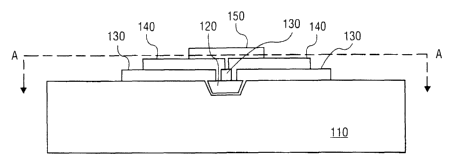
[042] Figure 1 illustrates a side view of an embodiment of a
strap, including a substrate with an embedded Nanoblock IC,
planarizing layer,and conductive medium that contacts the pad on the
NanoBIockT"" IC. The substrate 110 has an opening in it to contain the
Nanoblock IC, and may be a flexible plastic substrate for example.
Nanoblock IC 120 is a Nanoblock IC formed via conventional VLSI. The
Nanoblock IC 120 may be embedded in the opening of the substrate
110 through FSA for example. Nanoblock IC 120 may have a variety of
functions or structures consistent with an integrated circuit. In one
embodiment, Nanoblock IC 120 includes circuitry suitable for receiving
radio signals from an external antenna and sending radio signals via
the external antenna. Moreover, in one embodiment, Nanoblock IC 120
may receive power from an external source via an external antenna, and
use such power to send a radio signal via the external antenna.
[043] Formed above Nanoblock IC 120 is planarization layer
130, which may be formed through a conventional thin-film deposition,
pattern and etch or other similar method, and which may be formed of
an insulating material such as silicon dioxide for example. Formed
above planarization layer 130 are two conductors 140, which may be
formed from a screen-printed electrically conductive paste for example,
and which occupy two contact holes in the planarization layer 130.
Preferably, the two conductors 140 attach to conductive pads of
Nanoblock IC 120, and the two conductors 140 preferably do not directly
connect to each other. Formed above conductors 140 is insulating
layer 150 which may be formed through a thin-film or thick-film process
for example, and may fill in space between the two conductors 140. As
will be appreciated, a conductor may in some instances connect to
CA 02474054 2004-07-22
WO 03/063211 PCT/US03/02115
-11-
multiple pads of an integrated circuit by design. One example of such a
situation is connecting all ground pads of an IC to a single conductor to
achieve a common ground potential.
[044J As will be appreciated, Nanoblock IC 120 may be formed
with sufficiently large pads as to allow for direct connection between the
two conductors and the Nanoblock IC, thereby avoiding the requirement
of an intervening conductor. As will also be appreciated, such a
structure will, in some embodiments, require direct (vertical) connection
between any large-scale component and the Nanoblock IC through the
conductive medium, as some conductive media have isotropic
conductivity. Furthermore, note that conductive media may include
metal particles suspended in a carrier, conductive polymers, paste,
silver ink, carbon-based conductors, solder, and other conductors.
Also, note that the large-scale component discussed in this application
may be an antenna, an electronic display or display electrode, a sensor,
a power source such as a battery or solar cell, or another logic or
memory device (such as but not limited to microprocessors, memory,
and other logic devices), for example.
[045J Figure 2 illustrates a side view of an embodiment of the
strap of Figure 1 as attached to a large-scale component. Conductors
270 each have a direct connection to one of the conductors 140, and
potentially having a connection to one or more of insulation layer 150,
planarization layer 130, and substrate 110. Attached to each of
conductors 270 are one of conductors 280, which may be conductive
pads of an antenna or conductive ends of an antenna for example.
Thus, as illustrated, each of conductors 280 may be said to be coupled
(electrically) to Nanoblock IC 120. Substrate 290 is the material in
which conductors 280 are embedded or to which conductors 280 are
attached, and is preferably insulating in nature.
CA 02474054 2004-07-22
WO 03/063211 PCT/US03/02115
-12-
[046] Space 260 is a space between the two conductors 270,
which may be occupied by substrate 290 and/or insulator 150, or may
be left as a void in the structure. It is important to note that in most
applications, each of the two conductors 270 would not be connected
directly to the other conductor 270, and a similar statement may be
made with respect to the two conductors 280.
[047] In one embodiment, the conductive medium 270 is an
electrically conductive tape (such as those available from the Sony
Corporation, including Sony DP1122, for example). Moreover, the
conductive tape may be isotropically or anisotropically conductive. Such
a conductive tape may be applied (adhered) by rolling the tape along a
row of straps, applying sufficient pressure and possibly heat to adhere
the tape to the straps, and then cutting the tape to separate the
individual straps. This may be done in various manners.
[048] Alternatively, the conductive medium 270 or 140 may be a
conductive paste (such as those available from Ablestick, including
Ablebond 8175A for example) which is put on the straps) through a
screen printing process for example. Such a paste may be screened
on to the straps at moderate resolutions relative to overall
manufacturing tolerances, thereby allowing for useful connection to
conductors 140. Furthermore, a conductive medium 270 may also be a
metal particles suspended in a carrier, a conductive polymer, a carbon-
based conductor, a solder, or other conductive medium as will be
appreciated by those skilled in the art.
[049] Figure 3A illustrates a view of an embodiment of the strap
of Figure 1 along the line A-A in the direction indicated. The various
overlaps between substrate 110, Nanoblock IC 120, planarization layer
130, conductors 140 and insulation layer 150 are all illustrated.
Moreover, contact holes 315 in the planarization layer 130 are
CA 02474054 2004-07-22
WO 03/063211 PCT/US03/02115
-13-
illustrated, thus making apparent the connection between conductors
140 and Nanoblock IC 120.
[050] Figure 3B illustrates a view of an embodiment of the
apparatus of Figure 2 along the line B-B in the direction indicated.
Illustrated are overlaps between conductive layers 140, insulation layer
150, and conductors 280. For clarity, substrate 110 is also shown and
substrate 290 is not shown.
[051] Figure 4 illustrates an embodiment of an antenna. Each
arm 455 is connected to antenna conductor pads 280. Note that in an
alternate embodiment, arms 455 may simply form conductor pads 280,
making them a single unitary structure of both arm and pad.
[052] Figure 5 illustrates an embodiment of a tape spool having
adhered thereon straps including Nanoblock ICs. Each strap 505 (of
which one exemplary strap 505 is labeled) is adhered to a pair of
electrically conductive tape strips 515. The tape strips 515 form part of
a larger spool which also includes through-holes 525 for purposes of
spooling. In one embodiment, the tape strips 515 may be
anisotropically conductive film (ACF), with the conductors of the straps
505 adhered to the ACF. In an alternate embodiment, the conductive
medium may be on a surface of the straps 505 opposite the surface
adhered to by tape strips 515. Moreover, the tape spools of either
embodiment may be formed with gaps between columns of straps
allowing for slitting the tape through the gap to produce a single column
of straps.
[053] Figure 6 illustrates an embodiment of a method of forming
an apparatus including both small-feature-size and large-feature-size
components. At block 610, the integrated circuits are fabricated, such
as through a conventional VLSI method. At block 620, the integrated
circuits are embedded into substrate(s). At block 630, processing for
CA 02474054 2004-07-22
WO 03/063211 PCT/US03/02115
-14-
purposes of forming planarization and insulation layers occurs, and a
thick-film insulator is formed (one skilled in the art will appreciate that a
thin-film insulation layer may also be formed). At block 640, conductive
medium is applied to the substrate, such as by screen printing on
paste or through other additive processes. At block 650, a large-scale
component is attached to the conductive medium. Note that in one
embodiment, the tape spool of Figure 5 may be used to attach a large
volume of straps to large-scale components by attaching each strap
individually and then cutting the tape after attachment. In an alternate
embodiment, the conductive medium 640 is applied directly to the
substrate embedded with ICs 620, omitting the insulating layer.
[054] Figure 7 illustrates an alternate embodiment of a method
of forming an apparatus including both small-feature-size and large-
feature-size components, with particular reference to fabrication of RF-
ID tags using Nanoblock ICs. At block 710, the Nanoblock ICs are
fabricated, such as through conventional VLSI methods. At block 720,
the Nanoblock ICs are embedded in substrates through FSA. At block
730, any necessary post-FSA processing for purposes of forming
planarization layers, and/or insulation layers occurs. In particular, at
least one thin-film dielectric is formed. As will be appreciated by one
skilled in the art, the thin-film dielectric may not be necessary in
alternative embodiments. At block 740, a first conductive medium is
applied to the substrates, such as in the form of a paste screened on to
the substrates for example, thus creating straps. At block 750,
electrically conductive tape is adhered to the conductive medium on the
straps. At block 760, antennas are attached to the straps, such that the
antennas are electrically coupled to the Nanoblock ICs of the
corresponding straps.
CA 02474054 2004-07-22
WO 03/063211 PCT/US03/02115
-15-
[055] Figure 8 illustrates an alternate embodiment of a strap
from a side view. As will be appreciated, the embodiment of Figure 8 is
similar to the embodiment of Figure 1. However, Figure 8 illustrates a
substrate 810, having embedded therein (in an opening) an integrated
circuit 820, with pads 825. Each pad has deposited thereon through
use of an additive process a conductive medium 840, such as a silver
ink for example. Usually, but not always, the conductive medium 840 is
deposited such that it contacts one and only one pad 825 directly, thus
allowing for separate conductors for each electrical contact of a circuit.
[056] Moreover, it will be appreciated that the size of the pads
825 may be greater than the size of similar pads on an integrated circuit
such as Nanoblock IC 120 of Figure 1, in that the pads 825 must
interface directly with material (the conductive medium 840) having a
much larger feature size than is common for VLSI devices. Note that in
one embodiment, the conductive medium 840 may be expected to have
an as-deposited thickness of approximately 10-15 Nms and a final
thickness on the order of 1 pm or less, and that pads 825 may have
minimum dimensions on the order of 20 x 20 Nms or more.
[057] Figure 9 illustrates yet another alternate embodiment of a
strap from a side view. Figure 9 illustrates a similar embodiment to that
of Figure 8, which further incorporates an insulator. Substrate 910
includes integrated circuit 920 embedded therein. Pads 925 are a part
of integrated circuit 920, and may be expected to have similar
dimensions to pads 825. Insulator (dielectric) 930 is deposited on
integrated circuit 920 through use of a thick film process. Insulator 930
may be expected to have a thickness on the order of 10 (microns). Also
deposited with an additive process is a conductive medium 940, which
covers both an insulator 930 and some portion of a pad 925, that
thereby allows for electrical contact between the integrated circuit 920
CA 02474054 2004-07-22
WO 03/063211 PCT/US03/02115
-16-
and a large scale component. Conductive medium 940 may be
expected to have similar characteristics to conductive medium 840.
[058] Figure 10 illustrates a side view of still another alternate
embodiment of a strap. In this embodiment, the insulator (1030) is a
thin-film insulator patterned with vias through which the conductive
medium (1040) may achieve contact with the pads (1025) of the
integrated circuit (1020). As will be appreciated, the vias require greater
precision in patterning than do any of the insulators of conductor
components of Figures 8 and 9. Moreover, as will be appreciated, the
substrate 1010 may have insulator 1030 covering nearly its whole
surface, rather than the limited areas of Figure 9. Additionally, it will be
appreciated that the pads 1025 may be smaller on integrated circuit
1020 than similar pads of integrated circuits 920 and 820.
[059] Figure 11 illustrates another alternate embodiment of a
method of forming an apparatus including both small-feature-size and
large-feature-size components. At block 1110, an integrated circuit is
embedded within a supporting substrate. At block 1120, a thin-film
insulator is applied to the substrate. At block 1130, the insulator is
patterned such as through a photolithographic thin-film process,
whereby portions of the insulator are removed to expose portions of the
substrate or integrated circuit, such as bond or conductive pads.
Further cleaning, such as washing away photoresist for example, may
be involved as part of application, patterning, or even in a post-etch
phase. Alternatively, as will be appreciated, a photosensitive insulator
or dielectric may be used, thereby eliminating the need for photoresist
for example.
[060] At block 1140, a conductive medium is applied to the
substrate, coating all or part of the insulator. At block 1150, the
conductive medium is processed (such as by heat curing, for example)
CA 02474054 2004-07-22
WO 03/063211 PCT/US03/02115
-17-
as necessary to form a proper conductor. Note that curing of silver ink
is known in the art to be possible at 90-100°C for some formulations
with a reasonable cure time for various manufacturing processes. It
will be appreciated that cure times do vary, and that those skilled in the
art may adapt cure processes to the needs of a surrounding
manufacturing process and the devices to be produced. At block 1160,
the large-scale component is attached to the conductive medium,
thereby achieving electrical coupling with the integrated circuit. Also
note that the final processing of the conductive medium of block 1160
may be performed after the large scale component is attached at block
1170.
[061] For the most part, the previous description has
concentrated on use of the invention in conjunction with attaching a
strap having embedded therein an integrated circuit to a separate large-
scale component. It will be appreciated that other embodiments exist in
which the separate large-scale component is not involved. In particular,
a large-feature-size component may be incorporated as part of the
strap, such as an embedded conductor acting as an antenna, or may
be formed on the strap as illustrated in Figures 12a and 12b. Printing
or otherwise using additive processing technology to form an antenna
1240 of the conductive medium on the strap is one option.
[062] Alternately, other large-feature-size components, such as
power sources, sensors, or logic devices for example may either be
formed on the strap or attached to the strap. Interconnecting a
Nanoblock IC with such large-feature-size components on the strap
may be accomplished through use of conductive medium 1440,
allowing for electrical coupling between the large-feature-size
components 1460 and the small-feature-size (Nanoblock IC for
example) components 1420, as in Figure 14. Moreover, a conductive
CA 02474054 2004-07-22
WO 03/063211 PCT/US03/02115
-18-
medium 1340 may be used to interconnect two or more small-feature-
size components embedded in a single substrate, such as two
Nanoblock ICs for example, as illustrated in Figure 13.
[063] Figure 12A illustrates a top view of another embodiment of
a substrate. Substrate 1210 may be a substrate such as those
discussed previously, including a flexible or rigid material. Integrated
circuit (IC) 1220 is embedded in an opening in substrate 1210.
Insulator 1230 is a layer of insulating material (or a dielectric layer) on
top of both substrate 1210 and IC 1220 and may have planarizing
properties. Contact holes 1215 are holes in the insulator 1230 above
contact pads of IC 1220, allowing for physical contact and electrical
connection between IC 1220 and conductive media 1240. Layer 1250
is another insulator or dielectric above portions of conductive media
1240, insulator 1220 and substrate 1210, and above all of IC 1220.
Note that the actual configuration of the various layers may vary
considerably. For example, conductive media 1240 is formed into two
arms of an antenna, such as may be useful for radio frequency
applications. However, batteries, sensors, power supplies, button
cells, and displays and display electrodes may also be formed through
use of conductive media and other materials.
[064J Figure 12B illustrates a side view of another embodiment
of a substrate. As is illustrated, conductive media 1240 occupies the
contact holes 1215 of Figure 12A to contact directly with IC 1220.
Furthermore, as will be appreciated, the segments illustrated with
respect to conductive media 1240 correspond to the various segments
of the antenna as it traces its path along the surface of the insulator
1230. Along these lines, it will be appreciated that the presence of the
insulator 1230 may not be necessary in some instances.
CA 02474054 2004-07-22
WO 03/063211 PCT/US03/02115
-19-
[065J Figure 13 illustrates a side view of yet another
embodiment of a substrate. Substrate 1310 includes first integrated
circuit (IC) 1320 and second integrated circuit (IC) 1325. Insulator 1330
is formed above IC 1320, IC 1325 and substrate 1310. Conductive
media 1340 is formed above insulator 1330, and contacts both IC 1320
and IC 1325. One portion of conductive media 1340 forms an electrical
connection between IC 1320 and IC 1325, thereby electrically coupling
IC 1320 to IC 1325. Above both IC 1320 and IC 1325 are formed
insulator layers 1350.
[066] Figure 14 illustrates a side view of still another
embodiment of a substrate. Substrate 1410 has embedded in an
opening therein an IC 1420. Formed above substrate 1410 and IC
1420 is insulator 1430. Formed above insulator 1430 and connected to
IC 1420 is conductive media 1440, a portion of which is connected to
sensor 1460, thereby electrically coupling IC 1420 to sensor 1460.
Formed above a portion of conductive media 1440 and insulator 1430
is insulator 1450, which may or may not be of the same material as
insulator 1430.
[067] In the foregoing detailed description, the method and
apparatus of the present invention has been described with reference
to specific exemplary embodiments thereof. It will, however, be evident
that various modifications and changes may be made thereto without
departing from the broader spirit and scope of the present invention. In
particular, the separate blocks of the various block diagrams represent
functional blocks of methods or apparatuses and are not necessarily
indicative of physical or logical separations or of an order of operation
inherent in the spirit and scope of the present invention. For example,
the various blocks of Figure 1 may be integrated into components, or
may be subdivided into components, and may alternately be formed in
CA 02474054 2004-07-22
WO 03/063211 PCT/US03/02115
-20-
different physical shapes from those illustrated. Similarly, the blocks of
Figure 6 (for example) represent portions of a method that, in some
embodiments, may be reordered or may be organized in parallel rather
than in a linear or step-wise fashion. The present specification and
figures are accordingly to be regarded as illustrative rather than
restrictive.