Note: Descriptions are shown in the official language in which they were submitted.
CA 02474560 2004-07-26
WO 03/065418 PCT/US03/03323
PLANAR AVALANCHE PHOTODIODE
FIELD OF INVENTION
[0001] The present invention relates to an avalanche photodiode, and in
particular to a mesa structure avalanche photodiode having a planar p-n
junction.
BACKGROUND AND SUMMARY OF THE INVENTION
[0002] Owing to the known interaction between photons and electrons, great
advances have been made in the field of photodetectors in recent years,
particularly
in those photodetectors that utilize semiconductor materials. One type of
semiconductor-based photodetector is termed an avalanche photodiode. This type
of structure is generally composed of a number of solid semiconductive
materials
that serve different purposes such as absorption and multiplication.
[0003] The avalanche photodiode structure provides the primary benefit of
large gain through the action of excited charge carriers that produce large
numbers
of electron-hole pairs in the multiplication layer. However, an avalanche
photodiode
is so efficient at producing large numbers of charge carriers that it runs the
risk of
becoming saturated, thus adversely affecting the bandwidth of the device. In
order
to prevent charge carrier breakdown, it is imperative that the electric field
be
regulated within the avalanche photodiode itself, and in particular it is
desirable to
have the electric field in the multiplication layer be significantly higher
than that in the
absorption layer.
[0004] Mesa avalanche photodiodes have exposed high field p-n junction that
are difficult to passivate using a layer of insulating material. Therefore,
standard
commercial InP/InGaAs avalanche photodiodes use planar diffused structures
which
CA 02474560 2004-07-26
WO 03/065418 PCT/US03/03323
bury the p-n junction, leading to robust, long lifetime devices. However,
these InP
avalanche photodiodes require extremely accurate diffusion control of both the
depth
and the doping density of the p-type semiconductor regions. This critical
control is
essential, since this diffusion controls the magnitude of the electric field
in the
multiplication region, the length of the avalanche region, as well as the
charge
control.
[0005] There are no truly planar InAlAs avalanche photodiodes that have
been proposed. An existing avalanche photodiode has an etched isolation ring
which
is etched down to expose the top of the high field avalanche region followed
by' a
deep titanium implant to further isolate the high field region. This is then
followed by
a zinc diffusion to contact the p-type semiconductor region. This is a very
complicated structure requiring critical etching and implant steps. In spite
of these
efforts, it is believed that the lifetime of this avalanche photodiode is ten
times
shorter than their standard planar avalanche photodiode and thus not
sufficient for
telecommunications use.
[0006] Therefore, there is a need in the art for a simple yet effective
avalanche photodiode that is capable of being produced cheaply and with
efficient
critical control. Accordingly, the present invention comprises a planar
avalanche
photodiode including a first n-type semiconductor layer defining a planar
contact
area, and a second n-type semiconductor layer having a p-type diffusion
region.
Further features of the structure include an n-type semiconductor
multiplication layer
and an n-type semiconductor absorption layer, and a p-type contact layer. The
p-
type diffusion region is disposed directly adjacent to the p-type contact
layer, thereby
decreasing the capacitance of the planar avalanche photodiode while increasing
the
2
CA 02474560 2010-05-21
speed, lifetime, and cost-effectiveness of the structure.
In accordance with one aspect of the present invention, there is provided a
planar avalanche photodiode comprising: a first n-type semiconductor layer; a
first
contact layer, the first contact layer being on the first n-type semiconductor
layer; a
second n-type semiconductor layer having a p-type diffusion region, the p-type
diffusion region having a smaller area than the second n-type semiconductor
layer;
a semiconductor multiplication layer positioned between the first and second n-
type
semiconductor layers; a semiconductor absorption layer positioned between the
semiconductor multiplication layer and the second n-type semiconductor layer;
a
p-type contact layer; wherein the p-type diffusion region is disposed directly
adjacent
to the p-type contact layer; and a charge control layer, the charge control
layer being
located between the semiconductor absorption layer and the semiconductor
multiplication layer, the charge control layer having a substantially uniform
thickness
and an area larger than the diffusion region.
Further embodiments and advantages of the present invention are discussed
below with reference to the figures.
BRIEF DESCRIPTION OF THE DRAWINGS
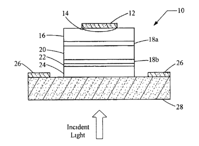
[0007] Figure 1 is a cross-sectional view of a planar avalanche photodiode in
accordance with a first embodiment of the present invention.
[0008] Figure 2 is a cross-sectional view of a planar avalanche photodiode in
accordance with an alternate embodiment of the present invention.
[0009] Figure 3 is a cross-sectional view of a mini-mesa planar avalanche
photodiode in accordance with an alternate embodiment of the present
invention.
3
CA 02474560 2010-05-21
DETAILED DESCRIPTION OF THE PREFERRED EMBODIMENT
[0010] In accordance with a preferred embodiment of the present invention,
an epitaxial structure is provided for photoconductive purposes. The
photoconductive structure is an avalanche photodiode that is optimized for
increased
performance through diffused p-type doping at a p-n junction. The particulars
of the
structure and method of manufacture of the present invention are discussed
further
herein.
[0011] Referring to Figure 1, a cross-sectional view of a planar avalanche
photodiode 10 is shown in accordance with a first embodiment of the present
invention. The planar avalanche photodiode 10 includes a p-type contact layer
12
and a first n-type semiconductor layer 28 providing a planar contact area. The
p-type
contact layer 12 is disposed on a second n-type semiconductor layer 16, which
includes a p-type diffusion region 14 for regulating the electric field at the
p-n
3a
CA 02474560 2004-07-26
WO 03/065418 PCT/US03/03323
junction formed by the p-type contact layer 12 and the second n-type
semiconductor
layer 16.
[0012] The planar avalanche photodiode 10 further includes an n-type
semiconductor absorption layer 20 that is separated from the second n-type
semiconductor layer by a first grading layer 18a. The n-type absorption layer
20 is
disposed on an n-type semiconductor multiplication layer 24. In a preferred
embodiment, the n-type semiconductor absorption layer 20 is separated from the
n-
type multiplication layer 24 by a p-type semiconductor charge control layer 22
and,
preferably, a second grading layer 18b. A pair of n-type contact layers 26 is
for
collecting electrons is shown disposed on the first n-type semiconductor layer
28.
[0013] The first n-type semiconductor layer 28 is selected from a group
comprising tertiary semiconductors, or group III-V semiconductors.
Accordingly, the
first n-type semiconductor layer 28 is either two elements from group III
combined
with one element from group V or the converse, two elements from group V
combined with one element from group III. A table of representative groups of
the
periodic table is shown below.
GROUP II GROUP III GROUP IV GROUP V
Zinc (Zn) Aluminum (AI) Silicon (Si) Phosphorus (P)
Cadmium (Cd) Gallium (Ga) Germanium (Ge) Arsenic (As)
Mercury (Hg) Indium (In) Antimony (Sb)
[0014] In the preferred embodiment, the first n-type semiconductor layer 28 is
InAlAs. However, it is understood that the first n-type semiconductor layer 28
may
4
CA 02474560 2004-07-26
WO 03/065418 PCT/US03/03323
be any tertiary semiconductor that provides the necessary bandgap for
optimized
operation of the planar avalanche photodiode 10.
[0015] The n-type semiconductor multiplication layer 24 is also selected from
a group comprising tertiary semiconductors, or group III-V semiconductors. In
the
preferred embodiment, the n-type semiconductor multiplication layer 24 is
InAIAs.
Preferably, the n-type semiconductor absorption layer 20 is also selected from
a
group comprising tertiary semiconductors, or group III-V semiconductors. In
the
preferred embodiment, the n-type semiconductor absorption layer 20 is InGaAs.
However, it is understood that both the n-type semiconductor absorption layer
20
and the n-type semiconductor multiplication layer 24 may be any tertiary
semiconductor that provides the necessary bandgap for optimized operation of
the
planar avalanche photodiode 10.
[0016] The second n-type semiconductor layer 16 is also selected from a
group comprising tertiary semiconductors, or group III-V semiconductors. As
before,
the second n-type semiconductor layer 16 is either two elements from group III
combined with one element from group V or the converse, two elements from
group
V combined with one element from group III. In the preferred embodiment, the
second n-type semiconductor layer 16 is InAlAs. However, it is understood that
the
second n-type semiconductor layer 18 may be any tertiary semiconductor that
provides the necessary bandgap for optimized operation of the planar avalanche
photodiode 10.
[0017] As noted, the second n-type semiconductor layer 16 defines in part a
p-type diffusion region 14 near the junction between the former and the p-type
contact area 12. The p-type diffusion region 14 lowers the capacitance of the
planar
CA 02474560 2004-07-26
WO 03/065418 PCT/US03/03323
avalanche photodiode 10 at the aforementioned p-n junction, thereby increasing
the
overall speed of the structure.
[0018] An aspect of the planar avalanche photodiode 10 is that all the
critical
layer thicknesses and doping concentrations are regulated in the initial
crystal
growth, and thus are under excellent control, can be reproducibly grown and
are
uniform over the entire wafer. Accordingly, difficulties associated with
process
control during fabrication, particularly those related the diffusion step, are
not
manifest in the present invention.
[0019] In another aspect of the present invention, shown in Figure 2, the
planar avalanche photodiode 110 includes a field control structure 30, such as
an n-
type implant or deep donor. The field control structure 30 is shown
schematically as
a pair of intrusions into the planar avalanche photodiode 110. However, in
practical
application, the field control structure 30 would consist of a region of the
planar
avalanche photodiode 110 that has undergone an implantation process, as
discussed further herein.
[0020] As in the first embodiment the invention, the planar avalanche
photodiode 110 includes the p-type contact layer 12 and the first n-type
semiconductor layer 28 providing a planar contact area. The p-type contact
layer 12
is disposed on the second n-type semiconductor layer 16, which includes the p-
type
diffusion region 14 for regulating the electric field at the p-n junction
formed by the p-
type contact layer 12 and the second n-type semiconductor layer 16. The field
control structure 30 provides additional electric field reduction around the
aforementioned p-n junction.
6
CA 02474560 2004-07-26
WO 03/065418 PCT/US03/03323
[0021] The field control structure 30 preferably takes the form of an
implanted
n-type semiconductor or ion. For example, the field control structure 30 may
take
the form of a region having Si infused into the planar avalanche photodiode
110.
Alternatively, a deep donor such as hydrogen or helium could be implanted in
the
region indicated by the field control structure 30. The effects of the field
control
structure 30 could also be realized through hydrogen passivation in the region
of
import. The field control structure 30 in its various forms will not penetrate
the n-type
semiconductor multiplication layer 24, as it is desirable to maintain a high
electric
field in this region.
[0022] In an alternate embodiment, shown in Figure 3, the planar avalanche
photodiode 210 includes a mini-mesa structure. As such, the second n-type
semiconductor layer described above is replaced with a p-type semiconductor
layer
32 that is epitaxially grown. Preferably, the p-type semiconductor layer 32 is
InAlAs,
but it is understood that the p-type semiconductor layer 32 may be any type
Ill-V
semiconductor that provides a suitable bandgap for optimized performance.
[0023] As in the prior embodiments, the planar avalanche photodiode 210
also includes the p-type contact layer 12 and the first n-type semiconductor
layer 28
providing a planar contact area. The p-type contact layer 12 is disposed on
the p-
type semiconductor layer 32. Passivated regions 34 are disposed in a
symmetrical
fashion about the p-type semiconductor layer 32 and the remaining structure of
the
planar avalanche photodiode.
[0024] In the embodiment shown in Figure 3 the full structure is grown
initially including the p-type semiconductor layer 32, and then it is etched
down to
the first n-type semiconductor absorption layer 20. The foregoing process
defines a
7
CA 02474560 2004-07-26
WO 03/065418 PCT/US03/03323
localized p- contact region which controls the relevant capacitance area, thus
resulting in a low capacitance and a high speed avalanche photodiode.
Moreover,
the entire planar avalanche photodiode 32 is epitaxially grown and does not
require
any p-type diffusion.
[0025] A particularly advantageous approach to form the passivated region 34
is to utilize wet oxidation. The p-type semiconductor layer 32 can be oxidized
through to one of the n-type semiconductor absorption layer 20 or the first
grading
layer 18a. Similarly, the sides of the outer mesa, which includes the n-type
semiconductor multiplication layer 24, the p-type semiconductor charge control
layer
22, and the second grading layer 18b, can be oxidized as indicated in Figure
3.
Finally, it is possible to oxidize the first n-type semiconductor layer 28 so
that there is
a gradual interface between the unoxidized and oxidized layers. This will
reduce the
field at the interface between the first n-type semiconductor layer 28 and the
n-type
semiconductor multiplication layer 24 leading to better passivation.
[0026] The passivation approach may be combined with proton or oxygen
implantation to additionally control the p-type semiconductor charge control
layer 22
and reduce the field at the edge of the outer mesa to further improve
passivation. A
suitable passivation technique includes the use of a surface passivation
material
such as BCB (benzocyclobutene). Alternatively, other surface passivation
materials
such as silicon dioxide, silicon nitride, or polyimide could be used to
passivate the
outside of the planar avalanche photodiode 210.
[0027] As described, the present invention provides numerous advantages
over existing avalanche photodiodes. Notably, the structure of the present
invention
is truly planar. Moreover, the structure of the planar avalanche photodiode 10
8
CA 02474560 2004-07-26
WO 03/065418 PCT/US03/03323
shown in Figure 1 is reversed from a typical InP/InGaAs avalanche photodiode
geometry since electrons are being avalanched in the n-type semiconductor
multiplication layer 24 as opposed to the avalanching of holes in an InP
multiplication region, as found in previous avalanche photodiodes. This
structural
inversion allows the low field region in the InGaAs absorption region to be at
the top
of the device rather than the high field avalanche region as in a standard InP
avalanche photodiode.
[0028] It should be apparent to those skilled in the art that the above-
described embodiments are merely illustrative of but a few of the many
possible
specific embodiments of the present invention. Numerous and various other
arrangements can be readily devised by those skilled in the art without
departing
from the spirit and scope of the invention as defined in the following claims.
9