Note: Descriptions are shown in the official language in which they were submitted.
CA 02474883 2004-08-03
WO 03/067637 PCT/US03/03602
METHODS OF TREATING A SILICON CARBIDE SUBSTRATE FOR IMPROVED
EPITAXIAL DEPOSITION AND RESULTING STRUCTURES AND DEVICES
Back r
To date, the most successful materials for producing light emitting devices or
"LEDs" (including light emitting diodes, laser diodes, photodetectors and the
like)
capable of operation in the UV, blue and green portions of the electromagnetic
spectrum have been the group III-nitride compound semiconductor materials, and
in
particular gallium nitride-based compound semiconductors. However, gallium
nitride presents a particular set of technical problems in manufacturing
working
devices. The primary problem is the lack of bulk single crystals of gallium
nitride
which in turn means that gallium nitride or other group Ill-nitride devices
must be
formed as epitaxial layers on other materials. Sapphire (i.e., aluminum oxide
or
A1203) has been commonly used as a substrate for group III-nitride devices.
Sapphire
offers a reasonable crystal lattice match to Group III nitrides, thermal
stability, and
transparency, all of which are generally useful in producing a light emitting
diode.
Sapphire offers the disadvantage, however, of being an electrical insulator.
This
means that the electric current that is passed through an LED to generate the
emission cannot be directed through the sapphire substrate. Thus, other types
of
connections to the LED must be made, such as placing both the cathode and
anode of
the device on the same side of the LED chip in a so-called "horizontal"
configuration.
In general, it is preferable for an LED to be fabricated on a conductive
substrate so
that ohmic contacts can be placed at opposite ends of the device. Such
devices,
called "vertical" devices, are preferred for a number of reasons, including
their easier
manufacture as compared to horizontal devices.
In contrast to sapphire, silicon carbide can be conductively doped, and
therefore can be effectively used to manufacture a vertical group III-nitride
LED. In
addition, silicon carbide has a relatively small lattice mismatch with gallium
nitride,
which means that high-quality group III-nitride material can be grown on it.
Silicon
carbide also has a high coefficient of thermal conductivity, which is
important for heat
dissipation in high-current devices such as laser diodes.
Examples of silicon carbide-based group III-nitride LEDs are shown in U.S.
Patents 5,523,589; 6,120,600; and 6,187,606 each of which is assigned to Cree,
Inc.,
CA 02474883 2004-08-03
WO 03/067637 PCT/US03/03602
2
the assignee of the present invention, and each of which is incorporated
herein by
reference. Such devices typically comprise a silicon carbide substrate, a
buffer layer
or region formed on the substrate, and a plurality of group III-nitride layers
forming a
p-n junction active region.
In particular, U.S. Patent No. 6,187,606 represents an important advance over
the state of the art as it previously existed. The invention described in the
'606 patent
provided a plurality of discrete crystal portions, or "dots," of GaN or InGaN
on the
substrate in an amount sufficient to minimize or eliminate the heterobarner
between
the substrate and the buffer layer. A highly conductive path between the
substrate and
the active region could thereby be established.
An important parameter for LEDs is the forward voltage (Vf) drop between the
anode and the cathode of the device during forward bias operation. In
particular, it is
desirable for the forward voltage (VF) of a device to be as low as possible to
reduce
power consumption and increase the overall efficiency of the device. Despite
the
advance of the '606 patent, there remains a measurable voltage drop at the
interface
between a conventional silicon carbide substrate and the conductive buffer
layer. It
is desirable to reduce this voltage drop in order to reduce the overall Vf of
the
resulting device.
Description
Methods according to embodiments of the present invention include the steps
of providing a SiC wafer having a predetermined conductivity type and first
and
second surfaces; implanting dopant atoms of the predetermined conductivity
type into
the first surface of the SiC wafer at one or more predetermined dopant
concentrations
and implant energies to form a dopant profile; annealing the implanted wafer;
and
growing an epitaxial layer on the implanted first surface of the substrate.
Other
methods according to embodiments of the present invention include the steps of
providing a SiC wafer having a predetermined conductivity type and first and
second
surfaces; forming a capping layer on the first surface of the wafer;
implanting dopant
atoms of the predetermined conductivity type into the capping layer and the
first
surface of the SiC wafer at one or more predetermined dopant concentrations
and
implant energies to form a dopant profile; annealing the implanted wafer;
removing
CA 02474883 2004-08-03
WO 03/067637 PCT/US03/03602
3
the capping layer; and growing an epitaxial layer on the implanted first
surface of the
substrate.
Structures according to embodiments the present invention include a silicon
carbide substrate having a predetermined conductivity type and having first
and
second surfaces with a first implantation profile of implanted dopants of the
predetermined conductivity type adjacent the first surface and an epitaxial
layer
grown on the first surface.
Devices according to embodiments of the present invention include a light
emitting device comprising a silicon carbide substrate having a predetermined
conductivity type and first and second surfaces, a conductive buffer layer on
the first
surface of the substrate, and an active region on the conductive buffer,
wherein the
first surface of the substrate has a first implantation profile of implanted
dopants of
the predetermined conductivity type adjacent the first surface.
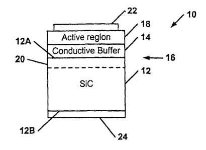
Refernng to FIG. 1 which shows a simplified schematic of a silicon carbide-
based LED according to the present invention, device 10 comprises a conductive
silicon carbide substrate 12 having a first conductivity type and having a
first surface
12A and a second surface 12B. Device 10 further includes a conductive buffer
region
14 formed on surface 12A of substrate 12 and an active region 18 formed on the
conductive buffer 14. Active region 18 preferably includes a p-n junction and
most
preferably comprises a single heterostructure, double heterostructure, single
quantum
well, multiple quantum well or the like. A first ohmic contact 22 is formed on
the
surface of the active region. A second ohmic contact 24 is formed on the
surface of
the substrate 24. In a preferred embodiment, substrate 12 comprises n-type 4H-
silicon
carbide. Accordingly, in a preferred embodiment ohmic contact 22 comprises the
anode of the device 10 while ohmic contact 24 comprises the cathode of the
device
10. Ohmic contact 24 may be formed according to the methods described in U.S.
Patent Application Serial No. 09/787,189 filed March 15, 2001, which is
incorporated
herein by reference. Substrate 12 includes a first implanted region 20
adjacent to
surface 12A and comprising implanted dopant atoms of the first conductivity
type.
The presence of implanted region 20 causes a reduction in the voltage drop
observable at the interface between substrate 12 and buffer region 14, which
results in
a reduction in the overall forward operating voltage (Vf) of the device 10.
The
CA 02474883 2004-08-03
WO 03/067637 PCT/US03/03602
4
implanted region has a peak concentration of implanted dopant atoms of between
about 1E19 and SE21 cm 3 and is between about 10 and 5000 ~ thick. Preferably,
the
implanted region has a peak concentration of implanted dopant atoms of about
1E21
cm 3 and is about 500 ~ thick.
FIG. 2 illustrates a method of fabrication of structures according to the
present
invention. A silicon carbide substrate 12 is provided having a first
conductivity type
and having first surface 12A and second surface 12B. The fabrication of doped
silicon carbide substrates such as substrate 12 is well known in the art. For
example,
U.S. Patent RE34,861 discloses a process for growing boules of silicon carbide
via
controlled seeded sublimation. The resulting silicon carbide crystal may
exhibit one
of a number of polytypes, such as 4H, 6H, 15R or others. N-type dopants such
as
nitrogen and/or phosphorus or p-type dopants such as aluminum and/or boron may
be
incorporated into the crystal during growth to impart a net n-type or p-type
conductivity, respectively. The crystal boules are then sliced into wafers
which are
chemically and mechanically treated (polished) to provide a suitable substrate
for the
growth of epitaxial layers and the fabrication of electronic devices thereon.
In a preferred embodiment, substrate 12 comprises n-type 4H or 6H-silicon
carbide doped with nitrogen donor atoms at a net dopant concentration of about
SE17
to 3E18 cm Z. Subsequent to wafering and polishing, dopant atoms 30 of a
predetermined conductivity type are implanted into surface 12A of substrate 12
at one
or more predetermined dopant concentrations and implant energies to form a
dopant
profile in implanted region 20 of substrate 12. Preferably, dopant atoms 30
have the
same conductivity type as substrate 12. That is, if substrate 12 is n-type,
then dopants
comprise a dopant such as nitrogen and/or phosphorus that imparts n-type
25 conductivity in silicon carbide. Alternatively, if substrate 12 is p-type,
then dopants
30 comprise a dopant such as boron or aluminum that imparts p-type
conductivity in
silicon carbide.
Dopants 30 are implanted into substrate 12 through surface 12A according to a
predetermined implant dose and energy level. Implantation may be performed in
one
30 step at a single dose and energy level or in a plurality of steps at
multiple doses and/or
multiple energy levels. In a preferred embodiment, implantation is performed
via a
plurality of implant doses and energy levels in order to impart a relatively
flat
CA 02474883 2004-08-03
WO 03/067637 PCT/US03/03602
implantation profile to a predetermined depth within substrate 12. For
example, in
one embodiment, a 6H-silicon carbide substrate is implanted with phosphorus
atoms
at a first dose of 2E15 cm 2 and an energy of 25 keV and a second dose of
3.6E15
cm z at an energy of 50 keV.
A schematic of a desired depth profile that could be formed according to this
embodiment is shown the graph of FIG. 4. The graph of FIG. 4 shows the profile
of
implanted atoms in atoms/cm3 (y-axis) as a function of depth in angstroms from
the
first surface 12A of substrate 12 (x-axis). As shown in FIG. 4, the implant
profile
increases to a maximum of about 1E21 cm 3 at a depth of about 300 ~. From
there,
the profile stays relatively flat to a depth of about 800 ~, and then begins
to drop off
to background levels. Accordingly, implanted region 20 may be said to extend
from
surface 12A into substrate 12 for a depth of about 800-1000 ~.
Following the implantation, the substrate is annealed in a standard tube
anneal
in Argon at a temperature of 1300° for 90 minutes to activate the
implanted dopants.
A range of temperatures is also effective for annealing, with 1300°
being exemplary
rather than limiting.
A conductive buffer 14 may then formed on surface 12A of substrate 12.
One drawback of this embodiment is that the dopant profile tends to reach its
maximum at some depth within the substrate, determined by the implant doses
and
energies. That is, the implant concentration at the surface is less than the
maximum
concentration within the substrate. Implanted dopant concentrations must be
kept at
less than about SE21 cm 3 or else the implanted atoms will cause unwanted and
irreparable damage to the crystal lattice of substrate 12.
In order to provide the maximum improvement in voltage drop, it is desirable
to have the implant concentration at the surface at the surface of the
substrate at as
high a level as possible, i.e., the implant concentration at the surface
should be around
1E21 cm 3. However, in order to achieve such a surface concentration according
to
the embodiment of FIG. 2, it would be necessary to implant the dopant atoms at
a
dose and energy level that would produce dopant concentrations within the
substrate
that would damage the substrate as described above.
Accordingly, in another embodiment of the invention illustrated in FIG. 3, a
capping layer 32 is deposited on surface 12A of substrate 12 prior to dopant
CA 02474883 2004-08-03
WO 03/067637 PCT/US03/03602
6
implantation. Preferably, capping layer 32 comprises a silicon nitride layer
or a
silicon dioxide layer deposited using Plasma-Enhanced Chemical Vapor
Deposition
(PECVD) or grown as a thermal oxide, both of which are well known processes
capable for depositing oxide layers of precise thickness and composition.
Capping
layer 32 may also comprise any other suitable material that may be
controllably
deposited in thin layers, is susceptible to ion implantation and can be
removed without
damaging the underlying surface. Other possible materials for capping layer 32
include a metal layer or an epitaxial semiconductor layer.
The thickness of capping layer 32 and the implantation parameters (dose and
energy) are selected such that the maximum implant concentration resulting
from the
implantation step occurs at or near the surface 12A of the substrate 12 (i.e.,
at or near
the interface between substrate 12 and capping layer 32). The resulting
structure is
then annealed in a standard tube anneal in argon at a temperature of
1300°C for 90
minutes to activate the implanted dopants. Capping layer 32 is removed using
conventional techniques. For example, if capping layer 32 comprises a PECVD
oxide
layer, it may be removed with a wet chemical etch process. The resulting
structure
then ideally comprises a substrate 12 having an implanted region 20 wherein
the peak
concentration of implanted atoms in the implanted region 20 occurs at or near
surface
12A of substrate 12.
A schematic of the desired depth profile that could be formed according to
this
embodiment is shown the graph of FIG. 5. The graph of FIG. 5 shows a schematic
profile of implanted atoms in atoms/cm3 (y-axis) as a function of depth in
angstroms
from the first surface 12A of substrate 12. As shown in FIG. 4, the implant
profile is
approximately 1E21 cm 3 at the surface 12A of the substrate 12. From there,
the
profile stays relatively flat for a depth of about 500 ~, and then begins to
drop off to
background levels.
In one embodiment, a silicon dioxide layer 32 having a thickness of about
500 ~ is formed via PECVD on surface 12A of substrate 12. Nitrogen atoms are
implanted into the oxide layer and the substrate 12 in a first dose at an
implant energy
of 25 keV and a second dose at an implant energy of 50 keV. The first implant
may
have a dose of about 4E12 cm 2 to 1E15 cm 2, while the second implant hay have
a
dose of about 7E12 cm 2 to 1.8E15 cm 2.
CA 02474883 2004-08-03
WO 03/067637 PCT/US03/03602
7
A graph of the interfacial voltage (Vf) at the substrate/buffer region
interface
versus 25keV implant dose is shown in Figure 6. To generate the data shown in
Figure 6, sample 4H and 6H silicon carbide wafers having a net concentration
of
nitrogen dopants of between 3.3E17 and 2.1E18 cm 3 were employed. A 500 ~
thick
S PECVD silicon dioxide layer was formed on the surface of the wafers, and the
wafers
were implanted with various controlled doses of nitrogen at energy levels of
25keV
and 50 keV respectively. The implant doses and energy levels for each wafer
are
shown in Table 1.
Table
1
Wafer T a Do ant 25 keV Dose cm' S0 keV Dose cm-
A 4H 28N2+ 2.SE14 4.38E14
B 4H 28N2+ 3.OE14 5.25E14
C 4H 28N2+ 3.SE14 6.13E14
D 4H 28N2+ 4.OE 14 7.OE 14
E 6H 28N2+ 2.SE14 4.38E14
F 6H 28N2+ 3.OE14 5.25E14
G 6H 28N2+ 3.SE14 6.13E14
Conductive buffers were then formed on the implanted substrates. The
interfacial voltage (i.e., the voltage drop attributable to the
substrate/buffer interface)
was measured at three locations on the wafer and an average value was
calculated.
The average values are plotted against the 25 keV implant dose in Figure 6. As
shown in Figure 6, the interfacial voltage of the substratelbuffer interface
decreases
with increasing dosage.