Note: Descriptions are shown in the official language in which they were submitted.
CA 02475191 2004-07-20
SYSTEM AND METHOD FOR RAPID READING OF
MACRO AND MICRO MATRICES
Field of the Invention
The present invention relates to a device for the reading and data analysis of
an assay
device for analysis of analytes.
Background of the Invention
Micro and macro matrices of bacteria and their respective toxic proteinaceous
contaminants account for several million cases of food-related illness and
about 9,000
deaths per year in the United States. Contaminated processed food, poultry and
meat
1o products etc. are a major cause of these deaths and illnesses. The five
most common
pathogens infecting food products and especially poultry and meat products are
E. coli
0157:H7, Salmonella species, Listeria species, Listeria monocytogenes and
Campylobacter jejuni.
Similarly, contamination of water supplies also causes illness and death. The
United
15 States Environmental Protection Agency has determined that the level of E.
coli in a
water supply is a good indicator of health risk. Other common indicators are
total
coliforms, fecal coliforms, fecal streptococci and enterococci. Currently,
water
samples are analyzed for these microorganisms with membrane filtration or
multiple-
tube fermentation techniques. Both types of tests are costly and time
consuming and
2o require significant handling. They are not, therefore, suitable for field-
testing.
Many disease conditions, such as bacterial and viral infections, many cancers,
heart
attacks and strokes, for example, may be detected through the testing of blood
and
other body fluids, such as saliva, urine, semen and feces for markers that
have been
shown to be associated with particular conditions. Early and rapid diagnosis
may be
25 the key to successful treatment. Standard medical tests for quantifying
markers, such
as ELISA-type assays, are time consuming and require relatively large volumes
of
fluid.
-1-
CA 02475191 2004-07-20
Accordingly, for the prevention of infection of consumers through contaminated
food
and water and detection of many disease conditions there is a need for the
accurate
and rapid identification of microorganisms and markers of the health of a
patient. The
accurate, rapid detection and measurement of microorganisms, such as bacteria,
viruses, fungi or other infectious organisms and indicators in food and water,
on
surfaces where food is prepared, and on other surfaces which should meet
sanitary
standards is, therefore, a pressing need in industrial, food, biological,
medical,
veterinary and environmental samples. Further, in routine inspection of
industrial
products for microbiological contamination there is a need for the eaxly
detection of
to contamination which will lead to more rapid release of safe products, and
for the
rapid, accurate detection and measurement of micro-organisms which are not
pathogenic but have a role in the determination of a product's shelf life.
A variety of assay methodologies have been used for determining the presence
of
analytes in a sample of interest. Assays for detecting some microorganisms
require
that the samples be cultured. In this assay, the typical practice is to
prepare a culture
growth medium (an enrichment culture) that will favour the growth of an
organism of
interest. A sample such as food, water or a bodily fluid that may contain the
organism
of interest is introduced into the enrichment culture medium. Typically, the
enrichment culture medium is an agar plate where the agar medium is enriched
with
2o certain nutrients. Appropriate conditions of temperature, pH and aeration
are provided
and the medium is then incubated. The culture medium is examined visually
after a
period of incubation to determine whether there has been any microbial growth.
It
could take several days to obtain results and requires a technician to read
the agar
plates by visual inspection which can lead to errors.
There are presently many examples of one-step assays and assay devices for
detecting
analytes in fluids. One common type of assay is the chromatographic assay,
wherein a
fluid sample is exposed to a chromatographic strip containing reagents. A
reaction
between a particular analyte and the reagent causes a colour change on the
strip,
indicating the presence of the analyte. In a pregnancy test device, for
example, a urine
3o sample is brought into contact with a test pad comprising a bibulous
chromatographic
strip containing reagents capable of reacting with and/or binding to human
chorionic
-2-
CA 02475191 2004-07-20
gonadotropin ("HCG"). The urine sample moves by capillary flow along the
bibulous
chromatography strip. The reaction typically generates a colour change, which
indicates that HCG is present. While the presence of a quantity of an analyte
above a
threshold may be determined, the actual amount or concentration of the analyte
is
unknown. Accordingly, there is a risk that a pathogen may be present below a
level
sufficient for either the test to detect its presence, or for the individual
assessing the
test strip to visually observe the colour change of the test strip.
Assays have been developed for providing a quantitative measure of the
presence of
pathogens or analytes of interest. In such a typical test assay, a fluid
sample is mixed
1o with a reagent, such as an antibody, specific to a particular analyte (the
substance
being tested for), such as an antigen. The reaction of the analyte with the
reagent may
result in a colour change that may be visually observed, or in
chemiluminescent,
bioluminescent or fluorescent species that may be observed with a microscope
or
detected by a photodetecting device, such as a spectrophotometer or
photomultiplier
15 tube. The reagent may also be a fluorescent or other such detectable-
labelled reagent
that binds to the analyte. Radiation that is scattered, reflected, transmitted
or absorbed
by the fluid sample may also be indicative of the identity and type of analyte
in the
fluid sample.
In a commonly used assay technique, two types of antibodies are used, both
specific to
20 the analyte. One type of antibody is immobilized on a solid support. The
other type of
antibody is labeled by conjugation with a detectable marker and mixed with the
sample. A complex between the first antibody, the substance being tested for
and the
second antibody is formed, immobilizing the marker. The marker may be an
enzyme,
or a fluorescent or radioactive marker, which may then be detected. See, for
example,
25 U.S. Pat. No. 5,610,077, which is incorporated herein by reference.
In order to quantitatively measure the concentration of an analyte in a sample
and to
compare test results, it is usually necessary to either use a consistent test
volume of the
fluid sample each time the assay is performed or to adjust the analyte
measurement for
the varying volumes.
-3-
CA 02475191 2004-07-20
There is therefore a need for a device which can efficiently, rapidly and
accurately
read an assay for determining the presence of analytes in a sample and for
determining
the quantity of respective analytes in the sample. There is a need for an
assay reading
device that permits a user to assess the results of the assay carned out in an
efficient,
simple and reliable manner.
Summary of the Invention
The present invention provides an analyte reading system which includes an
analyte
reader unit for rapidly detecting and evaluating the outcome of an assay to
measure the
presence of analytes in a sample. Quantitative and qualitative measurements of
1o analyte concentration in a sample may be rapidly obtained using the reader
device
with preset algorithms which also ascertain the nature of the assay being
read, provide
controls and can prevent erroneous duplication of measurement of that assay.
According to a method of the present invention, the reader device can detect
from a
reading area of an assay device control indicators from which the system can
calculate
15 or ascertain the nature of the assay or assays conducted in the assay
device, the
volume of sample and other control conditions such as the response of standard
samples to provide a reliable calibration within the assay device for the
analyte
reading system.
According to another aspect of the present invention, the reader device can
scan preset
20 areas of an assay device in order to provide focal points for the reader
device and
evaluate the volume of the test sample in the assay device. This aspect of the
invention permits the reader device to adjust the analyte measurement for
varying
volumes.
According to one aspect of the invention there is provided analyte reader unit
for
25 reading and measuring the outcome of an assay on an assay slide containing
a
fluorescently labelled analyte, comprising
a positioning stage for holding the assay slide in a desired position,
a light sensor, and
-4-
CA 02475191 2004-07-20
an optical system comprising
an excitation light source for illuminating a fluorescently labelled
analyte, and a dichroic mirror for reflecting excitation light to the
analyte and light emitted by the fluorescent dye to pass through to the
light sensor.
According to another aspect of the present invention, there is provided a
reading
system for reading and measuring the outcome of an assay on an assay slide
containing a fluorescently labelled analyte, comprising
a positioning stage for holding the assay slide in a desired position,
to a light sensor,
an optical system comprising
an excitation light source for illuminating a fluorescently labelled
analyte, and
a dichroic mirror for reflecting excitation light to the analyte and light
15 emitted by the fluorescent dye to pass through to the light sensor, and
a computer for processing the signal detected by the light sensor to generate
a
measurement of analyte density on a detected portion of the assay slide.
According to yet another aspect of the present invention, there is provided a
method of
reading an assay slide containing a fluorescently labelled analyte, comprising
the steps
20 of:
a. illuminating a portion of the assay slide containing a test sample.
b. detecting an intensity of light emitted by the test sample in a single
image
field, and
c. generating a measurement of analyte density in the test sample based on
said
25 intensity detection.
-5-
CA 02475191 2004-07-20
According to another aspect of the present invention, there is provided, a
method of
reading an assay slide containing a fluorescently labelled analyte, comprising
the steps
of
a. illuminating a portion of the assay slide containing a test sample of
unknown
analyte density and a portion of the assay slide containing a calibration
sample of
known analyte density with an excitation light,
b. detecting an intensity of light emitted by the test sample and an intensity
of
light emitted by the calibration sample in a single image field, and
c. comparing the intensity of light emitted by the test sample to the
intensity of
light emitted by the calibration sample to generate a measurement of analyte
density in
the test sample.
Brief Description of the Drawings
In drawings which illustrate by way of example only a preferred embodiment of
the
invention,
Figure 1 is a schematic view of an analyte reader system of the present
invention;
Figure 2 is a schematic view of the analyte reader of the invention;
Figure 3 is an assay device that can be read by the reading system of Figure
1;
Figure 4 is a reading portion of the assay device shown in Figure 3;
Figure 5 is a graph showing a relationship between fluorescent intensity of
test dots
and known antigen concentration in a sample;
Figure 6 is a graph showing a relationship between fluorescent intensity of
calibration
dots and the amount of antigen in the calibration dots;
Figure 7 is a graph showing a relationship between the antigen concentration
in the
sample and the amount of antigen in the calibration dots;
-6-
CA 02475191 2004-07-20
Detailed Description of the Invention
The present invention provides an analyte reading system and method for the
rapid
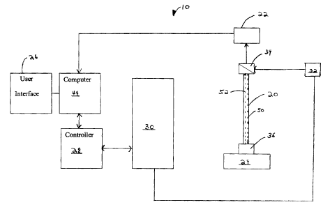
reading of macro and micro matrices such as that illustrated in Figure 1. As
illustrated
in Figure 1, in the preferred embodiment the analyte reading system 10
comprises a
analyte reading unit 20, which is preferably a microscope such as that
illustrated in
Figures 1 and 2, having an imaging device such as a CCD camera 22 which
transmits
signals to a general purpose computer 44 integrated into the system. The
microscope
20 has a stage 24. The stage movement (x and y axes) for assay positioning and
focusing (z axis) for image clarity and resolution are controlled by servo
motors
to through a suitable user interface 26, such as a touch-pad or touch-screen
control
board, which preferably also provides switches for the light sources. In the
preferred
embodiment the PC is programmed to process the signal returned by the CCD
camera
22 to provide accurate assay identification and results, as described in
detail below;
however the PC could also be programmed to control the functions of the
analyte
reading unit via suitable user displays and touch-screen activation of
functions. The
microscope has an optics assembly 62. Optics assemblies known in the art may
be
used for the purposes of the present invention. The microscope 20 also has a
dichromatic mirror 34 and a focus mechanism 36. A laser 32 is connected to the
dichromatic mirror 34.
2o The system 10 has a controller 28 that is connected to the computer 44. The
controller
28 is also connected to an options assembly 30. The options assembly 30
received
signals from the controller 28. The options assembly controls the laser 32
that is
adapted to apply energy to the dichromatic mirror 34 that forms part of the
microscope
20.
In operating the system, a user places an assay device that is to be read onto
the stage
24. The system then applies an initialization and calibration routine. The
assay device
preferably has an identification dot that is detected by the system and
provides
instructions regarding what assay is to be read and accordingly which routines
and
calculations need to be carried out. In reading an assay device, the laser 32
applies
light energy to the dichromatic mirror 34. Light beam 50 is reflected from the
CA 02475191 2004-07-20
dichromatic mirror 34 onto a sample on the stage 24. A return light beam is
reflected
off the sample to the CCD camera 22. The signal from the CCD camera 22 is
relayed
to the computer 44 where pre-programmed routines are performed on the image to
make the required calculations. The results of the calculations performed are
relayed
the user interface 26.
In one embodiment of the invention the analyte reading system is designed to
detect
microorganism antigens marked or coated with an indicator such as a
fluorescent
labelled antibody. In this embodiment the analyte reading system can be used
to
determine the concentration in a given sample of the microorganism antigen.
The
1o antigen concentration, which can be used as a measure of the microorganism
concentration from a sample, such as a food sample, can then be compared with
an
acceptable analyte concentration limit and a pass/fail response reported to
the user.
In this embodiment of the invention the analyte reader unit is adapted to read
and
detect specifically labelled analytes in an assay slide or assay chip in which
the analyte
15 sample is placed. One fluorescent dye suitable for labelling bacteria for
use in the
designed assay chip is Alexafluor~ 647nm dye. It is the assay chips which are
presented to the analyte reader for scanning. One skilled in the art will
appreciate that
alternatives to fluorescent labelling can also be used. Whatever labelling
system is
used, the light source (which may include electromagnetic radiation ranging
from
2o ultraviolet to infrared) for imaging and the detector must be matched, and
may be
collectively referred to as the imaging system.
In one embodiment of the invention the analyte reader unit, illustrated in
Figures 1
and 2, consists of seven parts: an optical system, a positioning stage, a
stage controller
board, an embedded computer, a monochrome CCD camera, a touch screen LCD
25 display, and a power supply board. In this embodiment the entire unit is
housed in a
case or containment means.
In a preferred embodiment the optical system consists of five parts: a light
source such
as a laser light source, a light emitting diode (LED) ring light source, a
filter cube, a
microscope objective lens, and an optical tube with focussing. In this
embodiment the
30 laser light source preferably has a peak spectral emission at 635 nm. The
laser spectral
_g_
CA 02475191 2004-07-20
emission at 635 nm then passes through an excitation filter of the filter
cube. This
excitation filter is used to control the bandwidth and wavelength of light
that will
reach the assay chip assay chip in the analyte reader unit. In this embodiment
the
excitation filter allows only the 635nm emission line from the laser light
source to be
passed to the filter cube's dichroic mirror, which then reflects this light
down the axis
of the optical tube towards the microscope objective lens. The laser light is
focused
on the assay chip assay chip by the microscope objective lens and causes the
labelling
marker, in this embodiment the Alexafluor~ 647nm fluorescent dye attached to
the
antibody bound (directly or indirectly) to the analyte to fluoresce and emit
light with a
1o peak intensity at 668nm.
In this embodiment a WSTech UH5-15G-635 lSmW 635nm laser diode module is
used to provide illumination of the assay chip for producing fluorescence of
the dye.
This is a class ITIb laser. However, a person skilled in the art will
appreciate that
different light sources, including different laser light sources, will be
suitable as an
excitation light source. The desirable laser will be dictated by the peak
emission
wavelength and the excitation wavelength for the labelling marker. As an
alternative
to laser illumination it is possible to use other excitation sources, for
example, an LED
or mercury vapour lamp, provided the desired excitation energy is transmitted
by that
light source in sufficient intensity to produce a detectable fluorescence in
the sample.
2o In this embodiment a custom moulded filter cube is used to hold the
excitation filter,
dichroic mirror, and emission filter in the most suitable position to allow
for
illumination of the assay chip from above through the microscope objective
lens. The
filter cube also preferably interlocks with the excitation light source via an
adjustable
flange. In this embodiment of the filter cube, a Chromate Technology
Corporation
Z635/20x 635nm (l2.Smm) narrow bandpass interference filter, is used as an
excitation filter. This filter has a full width-half maximum bandwidth of 20
nm. In
combination with this excitation filter a ChromaTM Technology Corporation
Z635RDC 635nm (20mmx30mm) dichroic mirror is used to reflect the laser light
down the axis of the optical tube towards the microscope objective. This
dichroic
3o mirror allows lower frequency light such as the light emitted from the
fluorescent dye
to pass straight through the dichroic mirror toward the image detector, in
this
-9-
CA 02475191 2004-07-20
embodiment a CCD camera comprising a CMOS image sensor. This embodiment of
the filter cube a Chromate Technology Corporation HQ685/SOm 685nm (25mm DIA)
bandpass filter is used as an emission filter. This filter has a full width-
half maximum
bandwidth of SOnm. This filter prevents any reflected laser light that passes
through
the dichroic mirror from reaching the CMOS image sensor. The sensor device is
held
in a fixed position relative to the filter cube. In this embodiment, a camera
board is
mounted to the top of the filter cube so that the image sensor is held in a
fixed
position relative to the filter cube.
The fluorescent emitted light is then focused by the microscope objective lens
as it
1o passes back up the optical tube to the dichroic minor. The fluorescent
light passes
through the dichroic mirror and then through the emission filter of the filter
cube. The
emission filter removes any reflected laser light in the image and allows only
the
fluorescent emitted light to pass to the image sensor device.
In a preferred embodiment of the invention, the assay chip containing the
labelled test
15 sample also has focus spots. To ensure accuracy in this embodiment of the
invention,
the analyte detector device ideally will focus the optical system by reference
to the
focus spots carried on the assay chip. When the analyte detector device is
focussing by
imaging the focus spots on the assay chip in this embodiment the laser light
source
used to provide the excitation of the labelled sample is prevented from
illuminating
2o the assay chip. This may be achieved in a variety of ways such as switching
off the
laser or blocking the light from the laser light source from entering the
filter cube. The
bright field illumination of the assay chip for imaging of the focus spots in
this
embodiment is provided by side illumination of the assay chip from the LED
ring light
source. In one embodiment the bright field side illumination of the assay chip
is
25 provided by four Lumex~ SSL-LX5093SRC/E 3500mcd 660nm high brightness
LEDs which are used in an LED ring around the microscope objective.
A suitable microscope objective lens for this embodiment of the invention is
an
Edmund Industrial OpticsTM R43-906 4x plan achromatic commercial grade
standard
microscope objective lens with a working distance of 13.9mm, which is used to
focus
-10-
CA 02475191 2004-07-20
an image of the bacteria on the CCD image sensor. This objective lens is
designed to
produce an image at 150mm from the top edge of the objective lens.
In this preferred embodiment of the device of the invention, a light-
impervious metal
optical tube is used to house the optics of the optical reading unit. The
purpose of this
optical tube is to prevent interference with the detected signal, the
excitation light and
emitted Light by peripheral or external Light sources. This optical tube is
grooved and
the entire assembly is anodized to reduce the reflection of light and prevent
reflection
of light from the optical assembly directly onto the image sensor. The optical
tube
provides a conduit for the light from the excitation source and the emitted
light from
the labelled analyte between the microscope objective lens and the filter
cube. In this
preferred embodiment the microscope objective lens is attached to the lower
end of
the optical tube and the filter cube is attached to the upper end of the
optical tube. One
way in which the filter cube and microscope objective lens can be attached to
the
optical tube is using threaded attachment.
In the preferred embodiment of the invention a Point Grey Research Dragonfly
IEEE-
1394 monochrome CCD camera is used to capture images of fluorescing analytes.
This camera contains an ICX204AL 1/3" black and white, 1024x768 pixel, CCD
image chip with a pixel size is 4.65um x 4.65um. The camera in this embodiment
is
powered from the IEEE-1394 bus and has an interface protocol which is
compliant
2o with the IEEE IIDC DCAM V 1.3 specification.
Thus, the analyte reading system of the invention can be used to carry out a
preferred
embodiment of the method of the invention, which comprises illuminating a
portion
of the assay slide containing a test sample of unknown analyte density and a
portion of
the assay slide containing a calibration sample of known analyte density with
the
excitation light; detecting an intensity of light emitted by the test sample
and an
intensity of light emitted by the calibration sample in a single image field;
and
comparing the intensity of light emitted by the test sample to the intensity
of light
emitted by the calibration sample to generate a measurement of analyte density
in the
test sample.
-11-
CA 02475191 2004-07-20
The optical tube is also provided with a focussing means, in this embodiment
using a
stepper motor focussing assembly. In an embodiment of the optical tube a
Hayden
Switch and Instruments 26463-12-003 26mm 12V captive unipolar linear actuator
stepper motor is used to move the lower end of the optical tube along the Z
axis. The
Z-axis is perpendicular to the plane defined by the assay chip in position on
the
positioning stage. Thus movement in this Z-axis provides focussing of the
microscope
objective lens on the assay chip.
A metal frame is used to keep the filter cube, optical tube, image board, and
positioning stage in fixed positions relative to each other. The positioning
stage is
1o used to move the assay chip in the X-Y plane relative to the microscope
objective
lens. The Y-axis is along the short dimension of the plane of the assay chip
which is
perpendicular to the longitudinal axis of the optical tube. The assay chip is
inserted
onto the positioning stage along the Y-axis of the assay chip. The X-axis is
along the
long axis of the plane of the assay chip which is perpendicular to the
longitudinal axis
15 of the optical tube. The positioning stage can be moved in the X-Y axis
using two
motors, for example two Hayden Switch & Instruments motors. In one embodiment
a 26mm 12V captive unipolar linear actuator stepper motor is used to drive the
stage
in the X-axis over a 12.7mm total displacement distance. Similarly, a 26mm 12V
non-captive unipolar linear actuator stepper motor is used to drive the stage
in the Y-
2o axis over a 38.1mm total displacement distance. These examples of motors
have a
step size of 0.005" (or approximately 12.7~m).
The reference (or home) position fox the positioning stage is found by moving
the
positioning stage to a preset position (usually to the limit of its range of
movement in
the X and Y-axes). At the reference position an electrical contact is
established with
25 two detector switches mounted on the positioning stage. One type of
detector switch
suitable for this application is PanasonicTM Type ESE11HS1. Optionally, the
positioning stage can be controllably moved to the locations of several
reference
marks or points on the assay chip for accurate optical calibration.
The positioning stage controller board (or stage controller board) controls
movement
30 of the positioning stage and controls the illumination of the assay chip
and positioning
-12-
CA 02475191 2004-07-20
stage by switching on or off the excitation light source (e.g. laser light
source), and by
switching on or off the side illumination light source (e.g. the ring LED).
Control of
the stage controller board is achieved by commands sent via an interface, e.g.
an
RS232 interface. Status messages are also sent back over the same interface.
The stage controller board in a preferred embodiment of the invention
comprises
several components and circuits: a microcontroller; an RS232 level converter;
stepper
motor drivers; a excitation light source driver or drivers; a side
illumination light-
source (or LED) driver; connectors and jumpers. In the preferred embodiment a
MicrochipTM PIC 16F876A-I/SP operating at l2MHz is used to control the
positioning
to stage. The microcontroller in this embodiment of the invention has the
following
features: 8Kx14 Flash program memory; 368x8 Data memory; 256x8 EEPROM
(Electrically Erasable Programmable Read-Only) memory; 22 general purpose I/O
lines (Input/output); watchdog timer; power on reset and brown out detector;
USART
(Universal Synchronous Asynchronous Receiver Transmitter); timers; and in-
circuit
serial programming
In the microcontroller of the above embodiment an ECS~ Inc. ECS-120-32-1 l2MHz
32pF parallel resonant crystal with an effective series resistance of 30ohms,
a 1mW
drive level, and a fundamental mode of vibration provides the
microcontroller's
internal oscillator circuit. The 22 general purpose I/O lines are as shown in
Table 1
below. If the microprocessor does not reset properly, if an infinite loop
occurs, if the
program counter gets lost, or if the timer interrupt ceases to be activated
then the
microcontroller is reset to a known state. This is achieved using an internal
watchdog
timer enabled with a prescaler of 1:128 to produce a watchdog timeout period
between
0.9s and 4.2s. If the watchdog timer is not cleared within this time period, a
reset is
generated. The watchdog timer is strobed once at the top of the main loop only
if the
timer interrupt has indicated that it is still running. The microcontroller's
built in reset
circuit is used to reset the microcontroller at powerup. In addition, an
internal
brownout detector will keep the microcontroller reset if the voltage drops
below about
4.OV and will reset the microcontroller once the voltage rises back within the
pre-
3o determined acceptable range.
-13-
CA 02475191 2004-07-20
In the microcontroller, the onboard USART is used to communicate with the
embedded computer. In this embodiment, the USART is set to run in full duplex
asynchronous mode using N-8-1 format (no parity, 8 data bits, 1 stop bit). The
baud
rate is set to 57600bps. The microcontroller also contains 3 timers, though in
this
embodiment only one of the timers is used. That timer is used to provide a
2.Sms
timer period to run the stepper motors. Three of the port B pins are
configured to
allow for in circuit programming of the microcontroller. Both high and low
voltage
programming modes are supported.
-14-
CA 02475191 2004-07-20
TABLE 1- I/O Line Use
I/O Line Type Function
RAO O X-axis, phase 0, driver 0
RA1 O X-axis, phase 0, driver 1
RA2 O X-axis, phase 1, driver 0
RA3 O X-axis, phase l, driver 1
1ZA4 O Unused
RAS O Z-axis, phase 0, driver 0
RBO O Unused
RB 1 O Laser driver
RB2 O LED driver
RB3 I PGM
RB4 O Z-axis, phase 0, driver 1
RBS I Z-axis home switch (focus)
RB6 I X-axis home switch (stage left-right)/PGC
RB7 I Y-axis home switch (stage front-back)/PGD
RCO O Y-axis, phase 0, driver 0
RC 1 O Y-axis, phase 0, driver 1
RC2 O Y-axis, phase 1, driver 0
-15-
CA 02475191 2004-07-20
I/O Line Type Function
RC3 O Y-axis, phase 1, driver 1
RC4 O Z-axis, phase l, driver 0
RCS O Z-axis, phase 1, driver 1
RC6 O DART Tx line
RC7 I UART Rx line
Also in this preferred embodiment, the RS232 level translation for the USART
serial
interface is provided by a Texas Instruments MAX232N SV only, 2 transmitter/2
receiver, RS232 driver. Two Texas InstrumentsTM ULN2003AN darlington
transistor
arrays are used to drive the three unipolar stepper motors. The stepper motors
are
powered from +12VDC. The common connection on the devices provides a
freewheeling path when the outputs to the stepper motors are turned off.
Diodes
Inc.~ SD 101 A schottky diodes are used as ground clamp diodes to prevent the
driver
outputs from going below ground potential. A Fairchild RFD14NOSL N-channel
logic
level power MOSFET is used to energize the laser light source used as the
excitation
light source for illumination of the assay chip. The laser is powered from
+SVDC. The
switching operation of the laser is controlled by application of a logic high
signal from
the general purpose UO pins to the gate of the MOSFET. A Fairchild RFD14NOSL N-
channel logic level power MOSFET is also used to energize the LED light source
used
for the side illumination of the assay chip. The LED is powered from +SVDC.
The
switching operation of the LED is also controlled by application of a logic
high signal
from the general purpose I/O pins to the gate of the MOSFET.
Several connectors are also required to make the electrical connections
between
components of the stage controller board:
-16-
CA 02475191 2004-07-20
1. A Molex 53109-0410 5.08mm right angle disk drive power connector is used
to provide power to the stage controller board. It mates with a standard PC
disk drive power cable connector. The pinout of the power connector is as
shown below in Table 2.
Table 2 - Pinout of Power Connector
Pin Function
1 +12VDC
2 GND
3 GND
4 +SVDC
2. An AMP 747844-6 female right angle DB9 connector is used to connect the
stage controller board to a computer serial port using a standard 9 pin serial
cable. This connector is configured as a DCE with null cable crossovers for
1o the control lines. The pinout of the 9-Pin Serial Connector is shown below
in
Table 3:
Table 3 - Pinout of 9 Pin Serial Connector
Pin Function
1 DCD, connected to 4 and 6
2 RD to PC
3 TD from PC
4 DTR, connected to 1 and 6
-17-
CA 02475191 2004-07-20
Pin Function
GND
6 DSR, connected to 1 and 4
7 RTS, connected to 8
8 CTS, connected to 7
9 RI, connected to GND
3. An AMP 499913-1 5x2 pin 0.1" right angle header with short latches provides
an alternate connection to a computer serial port. This connector allows a
straight through flat ribbon cable to connect directly to the COM2 port on VIA
EPIA M100001ME6000 motherboards. The pinout of the dual in-line 10 pin
serial port connector is shown below in Table 4:
Table 4 - Pinout of Dual in-Line 10 Pin Serial Port Connector
Pin Function
1 DCD, connected to 4 and 6
2 RD to PC
3 TD from PC
4 DTR, connected to 1 and 6
5 GND
6 DSR, connected to 1 and 4
7 RTS, connected to 8
-18-
CA 02475191 2004-07-20
Pin Function
8 CTS, connected to 7
9 RI, connected to GND
N/C
4. A JST S8B-EH 8 pin 2.Smm side entry shrouded header is used to connect the
positioning stage X-axis stepper motor and its associated limit switch to the
stage controller board. The mating connector is a JST EHR-8 female
receptacle housing with JST SHE-001 T-P0.6 crimp pins. The pinout of the X-
axis connector is as shown below in Table 5.
Table 5 - Pinout of X-axis Connector
Pin Function
1 X-axis phase 0, driver 0 (Black)
2 X-axis phase 0, power (White)
3 X-axis phase 0, driver 1 (Red)
4 X-axis phase l, driver 0 (Blue)
5 X-axis phase l, power (White)
6 X-axis phase 1, driver 1 (Green)
7 X-axis microswitch input
8 X-axis microswitch GND
5. A JST S8B-EH 8 pin 2.Smm side entry shrouded header is used to connect the
positioning stage Y-axis stepper motor and its associated limit switch to the
-19-
CA 02475191 2004-07-20
stage controller board. The mating connector is a JST EHR-8 female
receptacle housing with JST SHE-001 T-P0.6 crimp pins. The pinout of the Y-
axis connector is as shown below in Table 6.
Table 6 - Pinout of Y-axis Connector
Pin Function
1 Y-axis phase 0, driver 0 (Black)
2 Y-axis phase 0, power (White)
3 Y-axis phase 0, driver 1 (Red)
4 Y-axis phase 1, driver 0 (Blue)
Y-axis phase 1, power (White)
6 Y-axis phase l, driver 1 (Green)
7 Y-axis microswitch input
8 Y-axis microswitch GND
6. A JST S8B-EH 8 pin 2.Smm side entry shrouded header is used to connect the
focusing Z-axis stepper motor and its associated limit switch to the stage
controller board. The mating connector is a JST EHR-8 female receptacle
housing with JST SHE-001 T-P0.6 crimp pins. The pinout of the Z-axis
connector is as shown below in Table 7.
-20-
CA 02475191 2004-07-20
Table 7 - Pinout of Z-axis Connector
Pin Function
1 Z-axis phase 0, driver 0 (Black)
2 Z-axis phase 0, power (White)
3 Z-axis phase 0, driver 1 (Red)
4 Z-axis phase 1, driver 0 (Blue)
Z-axis phase 1, power (White)
6 Z-axis phase 1, driver 1 (Green)
7 Z-axis microswitch input
8 Z-axis microswitch GND
7. A JST S2B-EH 2 pin 2.Smm side entry shrouded header is used to connect the
laser to the stage controller board. The mating connector is a JST EHR-2
female receptacle housing with JST SHE-001 T-P0.6 crimp pins. The pinout
of the laser connector is as shown below in Table 8.
Table 8 - Pinout of Laser Connector
Pin Function
1 +SVDC to laser
2 Switched GND
8. A JST S2B-EH 2 pin 2.Smm side entry shrouded header is used to connect the
1o LED to the board. The mating connector is a JST EHR-2 female receptacle
-21-
CA 02475191 2004-07-20
housing with JST SHE-001 T-P0.6 crimp pins. The pinout of the LED
connector is as shown below in Table 9.
Table 9 - Pinout of LED Connector
Pin Function
1 Power to LED (current limited)
2 Switched GND
9. A JST S6B-EH 6 pin 2.Smm side entry shrouded header is used to allow in-
circuit serial programming of the microcontroller. The mating connector is a
JST EHR-6 female receptacle housing with JST SHE-OO1T-P0.6 crimp pins.
The pinout of the in-circuit serial programming connector is as shown below
in Table 10.
1o Table 10 - Pinout of IN-circuit Serial Programming Connector
Pin Function
1 VPP
2 VDD
3 VSS
4 RB7
1Z.B6
6 RB3
-22-
CA 02475191 2004-07-20
ICSP programming configuration jumpers are used to isolate the microcontroller
from
the rest of the system and connect the programming pins to the ICSP connector.
A
Molex 10-88-1081 0.100" 4x2 pin header is used to select programming or normal
mode. The valid jumper configurations are shown below in Table 11.
Table 11- Valid Jumper Configurations
Configuration Jumpers Installed
Programming mode 1-2, 5-6
Normal mode 3-4, 7-8
The Stage Controller Board software consists of a main loop that processes
commands
sent to it through the RS232 interface. After reset, the microcontroller
hardware is
configured, the data structures are initialized, and then the main loop is
entered. The
1o main loop is run until power is removed from the system. The commands sent
to the
Stage Controller Board through the RS232 interface consist of single functions
such
as moving an axis to a new position, getting the current position of an axis,
moving an
axis to the home position, and getting the current status of the stage
controller system.
In response to these commands, the Stage Controller Board performs the desired
15 action and sends back a confirmation or status information.
The main loop performs several functions including for example, re-
initializing the
configurable hardware or strobing the watchdog timer. In the preferred
embodiment
the main loop executes commands from the RS232 interface in a state machine
format. This prevents commands that take longer to execute from allowing the
2o watchdog timer to time out.
In addition to the main loop there are various interrupt routines that provide
realtime
control of the stepper motors and manage communications over the RS232 port.
For
example a timer interrupt routine can be set to trigger when the timer
comparator
postscaler overflows. This interrupt routine is used to generate the timing
for the
- 23 -
CA 02475191 2004-07-20
stepper motor outputs. In this example the timer interrupt routine, when
triggered,
would set the timer watchdog timer flag; check and store status of home
position
sensors; if any stepper motors have finished moving then clear their movement
commands; if any stepper motors are being calibrated then update calibration
status
based on movement commands and home position sensor status; update stepper
motor
outputs based on their movement command; and update stepper motor position
registers.
A preferred embodiment of the invention includes an embedded computer which is
responsible for the GUI interface and all of the processing done in the
system. The
1o internal computer connects to all of the peripheral components of the
system and
coordinates their fimctioning. In one preferred embodiment a Via Technologies
Inc.
EPIA M10000 mini-ITX PC mainboard is used as the embedded computer. In
addition, in this preferred embodiment there will also be a hard drive (e.g. a
Seagate
ST92011A, 20GB, 5400 rpm Notebook hard drive), a RS232 dual serial port card
(e.g.
15 an Axxon Computer Corporation MAP/950 PRO Dual 16950 RS232 PCI serial card
plugged into the PCI slot to provide a third and fourth RS232 serial port for
the
system); and DDR SDRAM memory (e.g Infineon DDR 256MB, 266MHz (PC2100)
184 Pin Memory) which provides all the main memory required by the CPU. The
computer may alternatively be a suitably programmed personal computer (PC), or
a
2o specialized computer with an ASIC cpu designed specifically for the analyte
reading
system.
The analyte reader system also requires a power supply. In the preferred
embodiment
of the analyte reader system described above an Ituner Networks Corp. PW70-A
DC-
DC converter is used to generate the voltages required by the system from a
single
25 12VDC source. The DC-DC converter produces ATX compatible voltages. The
maximum combined output power of this embodiment of the analyte reader system
is
100W. Alternatively an Ituner Networks Corp. AC-DC 12V, SA switching power
adapter is used to produce a 12VDC input to the DC-DC converter from a
110V/220V
AC outlet. This provides the analyte reader system with a maximum of
approximately
30 60W of power. Finally, the unit can also be powered from a 12VDC power
adapter or
-24-
CA 02475191 2004-07-20
vehicle 12VDC auxiliary outlet. In this way, the 12VDC is fed into the power
supply
board to provide the voltages needed by the analyte reader system.
In one embodiment of the device of the invention a housing unit is used for
the reader
system. A modified Digiconcepts Digital 917J Beige ATX 300W Midi Tower Case
can be used to house the reader system. A custom made bezel is then used to
mount
the LCD screen and touchpad in the three 5.25" drive bay slots in the front of
the case.
A touchscreen LCD such as an Apollo Display Technologies Ki-lA-063 5.7"
320x240
QVGA colour LCD touchscreen can be used to provide a user interface to the
system.
In this example embodiment the touchscreen LCD is powered from +5V and +12V
1o from the power supply and interfaces to the embedded PC through 2 RS232
serial
ports. During operation the assay chip containing the dye stained bacteria is
placed
into the reader and a start command is given via the touchscreen. The reader
then
scans the slide and counts the bacteria. Finally the result is displayed on
the display
and the assay chip can then be ejected and removed by the user. Examples of
other
15 commands that can be sent to the RS 232 interface in a preferred embodiment
include:
a "cancel" command which flushes the serial communications buffers and cancels
any
commands in progress; a "read status" command which reads the Stage Controller
Board status; a "clear error" command which clears the error status bit; a
"read axis
position" command which reads the current position of the specified axis; a
"calibrate
2o axis" command which calibrates the specified axis by moving it to the home
position;
a "move axis absolute" command which moves the specified axis to an absolute
position relative to the calibrated home position; a "move axis relative"
command
which moves the specified axis to a position relative to its current position;
a "set laser
mode" command which sets the laser mode to on or off; and a "set LED mode"
25 command which sets the LED mode to on or off.
The system of the present invention is typically employed to read the results
of assays
for the presence of microbes although the reader can also be used to read the
results of
assays for non-biological assays. One such as assay device that is useful for
biological
assays is shown in Figure 3. The assay device 70, has a substantially planar
surface 72
3o having a sample loading portion for receiving a fluid sample and reading
portion 80 as
-25-
CA 02475191 2004-07-20
shown in Figure 4. The assay device preferably has microspheres 74 at the
junction
between the sample loading and reading portions and act as a dynamic filter.
The
reading portion has printed thereon at least one and preferably at least two
test dots 86.
More preferably, a plurality of test dots 86 for detecting the presence of the
analyte are
s printed on the reading area 80. The test dots include a reagent that
specifically bind to
the analyte for which the assay is directed. The reagent is preferably a bound
antibody
specific for the analyte. The bound antibodies are preferably spaced apart to
make
each bound antibody available for binding to the test antigen free of stearic
hindrance
from adjacent antigen complexes. Preferably, a non-reactive protein separates
the
1o bound antibodies in the test dots.
The reading area 16 has calibration dots 84 printed thereon. The calibration
dots
include a pre-determined amount of said analyte for reacting with unreacted
reagent
form the vessel that is bound to a detectable marker. The calibration dots
allow the
intensity of the label to be correlated to the amount of the antigen present.
The
1s intensity of label in the test dots can then be used to derive the quantity
of antigen
present.
The results of the assay device 70 can be read and calculated by the reader
system of
the present invention. To determine the concentration of analyte in a sample,
the
concentrations of two characteristic assay reagents are predetermined. A
relationship
2o between a fluorescent intensity of the fixed test dots in a series of
samples with known
antigen concentrations is determined. An example of a relationship between
fluorescent intensity of test dots and known antigen concentration is a sample
is
shown in the form a graph as shown in Figure 5 Next, a relationship between
fluorescent intensity of the calibration dots and the amount of antigen in the
25 calibration dots, determined by using excess detection antibody, as shown
in Figure 6.
From Figure 5 and Figure 6, an association between the antigen in the sample
and the
antigen dot concentration is determined as shown in Figure 7. This calibration
curve
serves as a batch-specific standard curve for the determination of the antigen
concentration in the samples. The calibration curve is calculated by the
reader system
3o of the present invention based on the light intensities of the calibration
dots containing
known amounts of analyte.
-26-
CA 02475191 2004-07-20
In the instance of a sample of unknown antigen concentration, the sample is
premixed
with an excess of detecting antibody. This solution is applied to an assay
device such
as the assay device shown in Figure 3. The fluorescent intensity of the test
dots is
normalized against the calibration curve for that particular analyte to
provide a
normalized test dot value. This normalized test dot value is then read off the
calibration curve shown in Figure 7 for that analyte to give the concentration
of
analyte in the sample.
Those skilled in the art will recognize, or be able to ascertain using no more
than
routine experimentation, many equivalents to the embodiments of the invention
to described specifically above. Such equivalents are intended to be
encompassed in the
scope of the following claims,
-27-