Note: Descriptions are shown in the official language in which they were submitted.
CA 02475473 2011-04-12
METHOD OF COMMUTATING AN ELECTRONICALLY
COMMUTATED MOTOR AND MOTOR FOR CARRYING
OUT SAID METHOD
The invention concerns a method for commutating an electronically
commutated motor, and a motor for carrying out such a method.
Electronically commutated motors operate with a stator winding that has a
small number of phases. The motors principally used have one, two, or three
phases.
These phases can have power supplied to them in different ways depending on
the
type of electronics; supplying power via a full bridge circuit offers
particular
advantages.
With a full bridge circuit, steps must be taken to ensure that a short circuit
does not occur in the full bridge. There are numerous circuits for this, for
example the
circuit according to U.S. Pat. No. 4,376,261, which is based on the principle
of
creating a small gap between two control pulses. When the full bridge is
controlled
via a microprocessor ( P), corresponding current off-times can thus be "built
into" the
program, ensuring that upon commutation the one transistor switches off, then
there is
a delay of, for example, 50 s, and only then is the other transistor switched
on. A
prerequisite for this, however, is that a microprocessor be used, and this is
too
expensive for many applications. The current off-time of, for example, 50 s
must
furthermore be made so long that is sufficiently long under all operating
conditions,
with the result that, especially at higher rotation speeds, power output may
be
"wasted" because the current off-time could be shorter under many operating
conditions.
It is therefore an object of the invention to make available a novel method
for
commutating an electronically commutated motor, and a motor having a full
bridge
circuit for carrying out such a method.
According to the invention, this object is achieved by feeding a rotor
position
signal to a comparator which controls when a bridge transistor turns OFF,
monitoring
the gate potential of the transistor being turned off, to determine when to
turn ON the
next transistor, and using another comparator to turn ON that next transistor.
A
- 1 -
CA 02475473 2011-04-12
comparator is thus associated with each MOSFET of the bridge. When one of
these
MOSFETs is to be switched off, this occurs directly by way of its comparator.
When
one of these MOSFETs is to be switched on, the associated comparator then
monitors
the gate potential of the MOSFET that is to be switched off, i.e., in
practice, its
source-gate voltage. A reliable signal is thereby obtained as to when that
MOSFET is
blocked, and only then is the MOSFET that is to be switched on, switched on.
It is
very advantageous that with this method, the comparators are utilized
differently
depending on their instantaneous function (switching off or switching on),
i.e. in one
case as an amplifier, in the other as a comparator. The power output of such a
motor
can moreover be increased in many cases by optimizing the current off-time.
The stated object is achieved in a different fashion by controlling current
flow
through the winding phase using a p-channel MOSFET between the positive lead
and
the winding, and an n-channel MOSFET between the winding and the negative
lead,
with each MOSFET being controlled by a respective comparator, one of the
comparators responding to the rotor position signal, and the other of the
comparators
responding to a gate voltage of the transistor being switched off. A motor of
this kind
combines reliable commutation with a very simple and inexpensive
configuration,
good power output, quiet operation, and a long service life for the MOSFETs in
the
full bridge circuit. Further details and advantageous refinements of the
invention are
evident from the exemplary embodiment, in no way to be understood as a
limitation
of the invention, that is described below and depicted in the drawings, and
from the
dependent claims. In the drawings:
FIG. 1 is a circuit diagram of a preferred embodiment of an electronically
commutated motor for carrying out a method according to the present invention;
FIG. 2 is a diagram showing pulse sequences ul and u2, to explain FIG. 1; and
FIG. 3 is a circuit diagram to explain, by way of example, the generation of
two opposite-phase rotor position signals ul, u2, the amplitudes of which
depend on
the operating voltage UB of the motor.
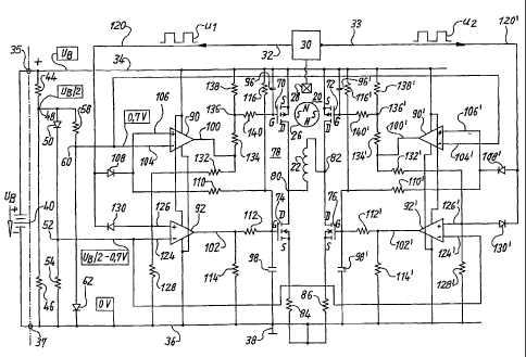
FIG. I shows, for explanation of the invention, a single-phase two-pulse
electronically commutated motor 20 having a single stator winding phase 22,
also
-2-
CA 02475473 2011-04-12
having a permanent-magnet rotor 26 that is depicted as a four-pole rotor, and
having a
Hall generator 28 whose output signal is fed to an arrangement 30 having an
output 32
and an output 33 antivalent thereto. In arrangement 30, the output signal of
Hall
generator 28 is converted into two square-wave signals ul and u2, which are
depicted
in FIG. 2 and proceed in oppositely-phased fashion. These can, if necessary,
be shifted
in phase in known fashion as a function of the rotation speed of motor 20;
this is not
depicted.
Motor 20 is supplied with voltage via a positive connecting lead 34 and a
negative connecting lead 36 that is usually connected to ground 38. Leads 34,
36 can
be connected via respective connecting terminals 35 and 37 to a battery 40
whose
voltage is labeled UB and is usually, in this case, in the range between 5 and
32 V. The
leads can also be powered from a rectifier, and are also referred to as a "DC
link"
circuit.
Located between leads 34 and 36 is a voltage divider having, for example, two
identical resistors 44, 46, so that a potential of approximately UB/2, i.e.
slightly less
than half the operating voltage, is present at their connecting point 48. The
amplitude
of pulses ul and u2 is a function of UB and is preferably also equal to UB/2.
Node 48 is connected to the anode of a diode 50 whose cathode is connected
via a node 52 and a resistor 54 to negative lead 36. A potential of
approximately
(UB/2 - 0.7 V) (1),
is thus obtained at node 52, i.e. lower than the potential UB/2 by an amount
equal to
the threshold voltage of diode 50 (approx. 0.7 V); this means that when
operating
voltage UB changes (for example, because battery 40 is deeply discharged), the
potential UB/2 at node 48 changes and the potential (UB/2 - 0.7 V) at node 52
likewise
changes, so that these potentials change, but a difference between nodes 48
and 52 of
approx. 0.7 V is maintained.
Node 48 is also connected via a resistor 58 and a node 60 to the anode of a
diode 62 whose cathode is connected to negative lead 36. The result is a
potential at
node 60 that is approximately 0.7 V higher than the potential (0 V) of lead
36.
Four MOSFET transistors serve to control the current in phase 22 of motor 20,
namely a p-channel MOSFET 70 at upper left, a p-channel MOSFET 72 at upper
-3-
CA 02475473 2011-04-12
right, an n-channel MOSFET 74 at lower left, and an n-channel MOSFET 76 at
lower
right. The four transistors 70 through 76 together constitute a full bridge
circuit 78 in
the form of an H-bridge. This is constituted by two half bridges, namely the
left
MOSFETs 70 and 74 on the one hand, and the right MOSFETs 72 and 76 on the
other
hand. Source S of transistors 70 and 72 is connected to positive lead 34.
Drain
terminals D of transistors 70 and 74 are connected to a node 80 and to a
terminal of
winding phase 22. Drain terminals D of transistors 72 and 76 are connected to
a node
82 and to the other terminal of winding phase 22. Source S of transistor 74 is
connected via a resistor 84 to negative lead 36, and source S of transistor 76
thereto
via a resistor 86. Resistors 84 and 86 can serve for current measurement, e.g.
for a
current limiter (not depicted). If this is not desired, these resistors can be
omitted.
When transistors 70 and 76 are conductive, a current flows from positive lead
34 through transistor 70 and terminal 80 to phase 22, and on through
transistor 76 and
resistor 86 to negative lead 36. When transistors 72 and 74 are conductive, on
the
other hand, a current then flows from positive lead 34 through transistor 72,
terminal
82, winding phase 22, transistor 74, and resistor 84 to negative lead 36.
During the switchover between these two states, it must not happen that
transistors 70 and 74 are simultaneously conductive for a short period of
time, or that
transistors 72 and 76 are briefly both conductive, since the resulting short-
circuit (or
"shoot-through") current would destroy these transistors or at least shorten
their
service life. The present invention is intended to prevent or at least greatly
reduce this.
A comparator 90 serves to control upper left transistor 70, and a comparator
92
to control lower left transistor 74. In FIG. 1 the right half of the circuit
is symmetrical
to the left half, and the components there are therefore labeled identically
but with an
appended apostrophe ('). Upper right transistor 72 is thus controlled by a
comparator
90', and lower right transistor 76 by a comparator 92'. (The additional
components on
the right side are not described. For them, the reader is referred to the
description of
the left side of FIG. 1.)
Gate G of transistor 70 is connected via a capacitor 96, and gate G of
transistor
72 via a capacitor 96, to positive lead 34. Gate G of transistor 74 is
connected via a
capacitor 98, and gate G of transistor 76 via a capacitor 98', to negative
lead 36. These
-4-
CA 02475473 2011-04-12
capacitors prevent abrupt changes in the voltage between source (S) and gate
(G) of
transistors 70 through 76 and, depending on their size, cause switching
operations to
become slower with the result that motor 20 runs more quietly.
SWITCHING P-CHANNEL TRANSISTORS 70 AND 72 ON AND OFF
When one of transistors 70 or 72 is to be switched on, its gate potential must
be modified in the direction toward negative lead 36; in other words, its
source-gate
voltage USG must be increased to a value in the preferred range 1.5 - 4 V,
maximum
20 V. In this case output 100 of upper comparator 90, or output 100' or upper
comparator 90', is therefore connected internally to negative lead 36, thus
causing
voltage USG to increase correspondingly because the potential at output 100
substantially determines the potential at the gate of transistor 70.
Conversely, when one of transistors 70 or 72 is to be switched off, its gate
potential must be modified in the direction toward positive lead 34, so that
USG
becomes less than 1.4 V. This is done by making output 100 or 100' high-
resistance.
The potential at gate G of the relevant transistor 70 or 72 thus changes in
the
positive direction during the transition from the switched-on to the switched-
off state,
and when USG falls below a predetermined value, this means that the relevant
transistor 70 or 72 is safely blocked, i.e. is in a high-resistance state.
SWITCHING N-CHANNEL TRANSISTORS 74 AND 76 ON AND OFF
When one of transistors 74 or 76 is to be switched on, its gate potential must
be modified in the direction toward positive lead 34, i.e. its gate-source
voltage UGS
must increase to a preferred value in the range 1.5 to 4 V, maximum 20 V. In
this case
output 102 of lower comparator 92, or output 102' of lower comparator 92', is
therefore made high-resistance, with the result that voltage UGS of the
relevant
transistor 74 or 76 rises, and the latter becomes conductive.
Conversely, when one of transistors 74 or 76 is to be switched off, output 102
or 102' is then connected to negative lead 36 so that UGS drops below 1.4 V
and the
relevant transistor 74 or 76 is blocked.
-5-
CA 02475473 2011-04-12
The potential at gate G of the relevant transistor 74 or 76 thus changes in
the
negative direction during the transition from the switched-on to the switched-
off state;
and when UGS falls below a predetermined value, this means that the relevant
transistor 74 or 76 is blocked, i.e. is in its high-resistance state.
Negative input 104 of upper comparator 90, like negative input 104' of
comparator 90', is connected to node 60, i.e. is at a potential of
approximately 0.7 V
with reference to negative lead 36. Positive input 106 of comparator 90 is
connected
to the cathode of a diode 108, and also via a resistor 110 to gate G of lower
left
transistor 74. This gate G is in turn connected via a resistor 112 to output
102 of lower
left comparator 92, and via a resistor 116 to positive lead 34. Output 102 is
also
connected via a resistor 114 to negative lead 36. The anode of diode 108 is
connected
to an input 120 to which is conveyed, during operation, a square-wave signal
ul (FIG.
2A) that is opposite in phase to a square-wave signal u2 (FIG. 2B) that is fed
to input
120'.
As FIG. 2 shows, in this example signals ul and u2 have an amplitude of UB/2
corresponding to the logical value "1 ", or of <0.4 V corresponding to the
logical value
"0". Amplitude UB/2 is thus a linear function of operating voltage UB (see
FIG. 3).
Negative input 124 of lower comparator 92, like negative input 124 of lower
comparator 92', is connected to node 52, at which a potential of approximately
(UB/2 -
0.7 V) is present, i.e. for example, for a voltage UB = 20 V, a potential of
approximately
(20/2 - 0.7) = 9.3 V (2).
Positive input 126 of comparator 92 is connected via a resistor 128 to
negative
lead 36, likewise to the anode of a diode 130 whose cathode is connected to
terminal
120. Input 126 is furthermore connected via a resistor 132 to output 100. The
latter is
connected via a resistor 134, a node 136, and a resistor 138 to positive lead
34. Node
136 is connected via a resistor 140 to gate G of upper transistor 70.
Preferred values of the components in FIG. 1 for a motor with UB = 24 V (k =
kilohm; R = resistor; C = capacitor):
Diodes 50, 62, 108, 108', 130, 130' basl6
Comparators 90, 90', 92, 92' LM2901
-6-
CA 02475473 2011-04-12
p-channel MOSFETs 70, 72 IRFR9024
n-channel MOSFETs 74, 76 IRFRO24
C 96, 96', 98, 98' 4 nF
R 44, 46 20 k
R 54, 58, 110, 110', 128, 128', 132, 132' 470 k
R134,134' 1.1 k
R114,114',136,136' 3k
R 116,116' 510 ohm
R 112,112', 140,140' 300 ohm
R84,86 0-0.1ohm
MODE OF OPERATION
The description of the mode of operation makes reference only to the left half
of FIG. 1, i.e. to the left half bridge. The right half is configured
identically and
therefore functions in the same way, but because signals ul and u2 are
opposite in
phase, processes on the right side occur with a 180-degree phase shift from
processes
on the left side, as one skilled in the art of electrical engineering will
readily
understand. For example, when upper left transistor 70 is switched on, lower
right
transistor 76 is switched on approximately simultaneously; and when upper
right
transistor 72 is switched on, lower left transistor 74 is switched on
approximately
simultaneously.
At time tl in FIG. 2A, signal ul at input 120 has a value of approx. 0.4 V,
diode 130 becomes conductive, and the potential at positive input 126
therefore
corresponds to the sum of that 0.4 V plus the voltage at diode 130 (approx.
0.7 V), i.e.
approximately 1.1 V in total. This is lower than the potential at negative
input 124,
which according to equations (1) and (2) is equal to (UB/2 - 0.7 V). Output
102 in
lower comparator 92 is therefore connected internally to ground 36, so that
the UGS
of transistor 74 is low and the latter is blocked.
The low potential at gate G of lower left transistor 74 is transferred through
resistor 110 to positive input 106 of upper comparator 90. This potential is
lower than
the potential (0.7 V) at negative input 104, so that output 100 of upper
comparator 90
-7-
CA 02475473 2011-04-12
is connected internally to ground 36. By way of voltage divider 134 (1.1 k)
and 138 (3
k), gate G of upper left transistor 70 acquires a potential of approx. 25% of
operating
voltage UB, so that at time tl transistor 70 is conductive while lower left
transistor 74
blocks.
At time t2 in FIG. 2A, signal ul changes from 0.4 V to UB/2. This causes the
previously conductive diode 130 to block, i.e. lower comparator 92 now serves
to
control the switching-on operation of lower left transistor 74 as a function
of the gate
potential of upper transistor 70. Diode 108 now becomes conductive, and as a
result a
potential of approximately (UB/2 - 0.7 V) is present at positive input 106 of
upper left
comparator 90. (The 0.7 V corresponds to the voltage at diode 108, and UB/2
corresponds to the amplitude of signal ul.) Since this potential (UB/2 - 0.7
V) is
higher than the reference potential of 0.7 V at negative input 104 of upper
comparator
90, the latter's output 100 becomes high-resistance, so that by way of the
voltage
divider made up of the four resistors 138, 134, 132, and 128, the potential at
gate G of
upper transistor 70 is pulled toward positive, and upper left transistor 70
consequently
blocks.
The increase in the potential at gate G of upper transistor 70 is somewhat
delayed by capacitor 96, i.e. this capacitor determines the rate of increase.
The
parasitic capacitances in transistor 70 also contribute to this. The increase
in the
potential at output 100 is transferred via (identically sized) resistors 132
and 128 to
positive input 126 of lower comparator 92. Only when this potential has
reached
approximately twice the value (UB/2 - 0.7 V), i.e. when upper transistor 70 is
safely
blocked, is lower comparator 92 switched over to high resistance so that the
voltage at
gate G of lower left transistor 74 rises sufficiently that that transistor
becomes
conductive. Resistor 110 causes the potential at positive input 106 of upper
comparator 90 to be raised so that the latter's output 100 remains at high
resistance,
and transistor 70 remains securely blocked.
It is thus evident that the change in potential at the gate of transistor 70
is
transferred to positive input 126 of lower comparator 92. The increase must be
somewhat greater than twice (UB/2 -0.7 V) because of voltage divider 128, 132,
and
lower transistor 74 is switched on when that is the case.
-8-
CA 02475473 2011-04-12
In this case, upper transistor 70 is therefore switched off directly by means
of
signal ul via upper diode 108, while lower diode 130 blocks and disconnects
lower
comparator 92 from signal ul, so that the latter component can delay the
switching-on
of transistor 74 until upper transistor 70 is safely blocked.
At time t3 (FIG. 2), signal ul changes from UB/2 to 0.4 V. As a result, diode
108 blocks, diode 130 becomes conductive, and positive input 126 of lower
comparator 92 receives a potential of approximately 0.4 V + 0.7 V = 1.1 V.
(The 0.7
V corresponds to the voltage at diode 130.) Output 102 of lower comparator 92
is
thereby connected internally to lead 36, causing transistor 74 to block (after
capacitor
98 discharges).
It should be noted here that the voltage values 0.4 V and 0.7 V are
approximate values for a quantitative example, and that different values may
occur in
reality.
The change in the potential at output 102 is transferred through resistors
112,
110 to positive input 106 of upper comparator 90. When the potential at input
106
becomes lower than the potential (0.7 V) at negative input 104, output 100 of
the
upper comparator is then pulled down to the potential of negative lead 36, so
that the
voltage USG between source and gate of upper transistor 70 rises
correspondingly and
the latter is switched on.
Upper transistor 70 is thus not switched on until the gate-source voltage UGS
of lower transistor 74 has dropped to a value below the reference voltage of
0.7 V at
positive input 104, i.e. when lower transistor 74 is in the safe, high-
resistance region.
Resistors 128, 132 cause positive input 126 to receive a lower potential, so
that the
output of comparator 92 remains low-resistance and keeps transistor 74
blocked. At
time t3, therefore, the previously conductive lower transistor 74 becomes
blocked, and
only when it is safely blocked is upper transistor 70 switched on.
It is evident that one of the two diodes 108, 130 serves respectively to block
one of the two transistors 70, 74 immediately when signal ul changes, while
the other
diode blocks and thereby allows the comparator associated with it to operate
as a
comparator. This comparator compares the (variable) potential at its positive
input
with a reference voltage that, in this example, is equal to 0.7 V for upper
comparator
-9-
CA 02475473 2011-04-12
90 and has a value of (UB/2 - 0.7 V) for lower comparator 92; in other words,
for
lower comparator 92, this reference voltage is a function of voltage UB and
changes
with it. This enables safe operation even when voltage UB changes greatly
during
operation, e.g. as a result of charging or discharging of backup battery 40
that is
depicted.
FIG. 3 shows an exemplifying embodiment for circuit 30 (FIG. 1) in a
simplified configuration in which the instant of commutation is not dependent
on
rotation speed.
FIG. 3 uses two comparators 150, 152 to whose inputs the output signal of
Hall generator 28 is conveyed, as depicted, with reversed polarity. The two
comparators 150, 152, like comparators 90, 92, are open-collector comparators,
i.e.
when the potential at the positive input of comparator 150 is higher than at
the
negative input, its output 32 is high-resistance; and when the potential at
the positive
input is lower than at the negative input, output 32 is connected internally
to negative
lead 36, so that a potential of approx. + 0.4V (with reference to negative
lead 36) is
obtained at output 32.
Output 32 is connected via a resistor 154 to positive lead 34, and via a
resistor
156 to negative lead 36. Resistors 154, 156 are identical in size, i.e. when
output 32 is
high-resistance, it acquires the potential UB/2 through resistors 154, 156.
The same applies analogously to comparator 152, whose output 33 is
connected via a resistor 158 to positive lead 34 and via a resistor 160 to
negative lead
36. Resistors 158, 160 are also identical in size, so that once again a
potential UB/2
exists at output 33 when that output is high-resistance, and a potential of
0.4 V when
that output is connected internally to negative lead 36.
The amplitude of signals ul, u2 is thus directly proportional to voltage UB,
which can vary within wide limits during operation.
Since the reference potential at node 52 of FIG. 1 is also dependent on
voltage
UB, i.e. has the value (UB/2 - 0.7 V) in accordance with equation (1), the
four
comparators 90, 90', 92, 92' can reliably control full bridge circuit 78 even
when
voltage UB changes. This is because the voltages that must be compared with
one
another using comparators 92, 92' change in the same direction. Instead of
UB/2 (i.e. a
-10-
CA 02475473 2011-04-12
factor of 0.5), a different factor such as 0.6 * UB or 0.4 * UB could of
course also be
selected, in which case resistors 44, 46, 128, 132, 154, 156, 158, and 160
would then
need to be adapted accordingly. The approach using a factor of 0.5 is
preferred,
however, because in this case identical resistors with low tolerances can be
used.
Many variants and modifications are, of course, possible within the scope of
the present invention.
-11-