Note: Descriptions are shown in the official language in which they were submitted.
CA 02475625 2004-07-23
JACKETED LED ASSEMBLIES AND LIGHT STRINGS CONTAINING SAME
This application is a Continuation-In-Part of U.S. Patent Application No.
10/243,835 filed September 16, 2002, which is a Continuation of U.S. Patent
Application
No. 09/819,736 filed March 29, 2001, now U.S. Patent No. 6,461,019.
BACKGROUND OF THE INVENTION
1. Field of Invention
The present invention relates to light emitting diode assemblies, light
strings
comprising a plurality of light emitting diode assemblies, and related
methods.
2. Description of Related Art
Light emitting diodes (LEDs) are increasingly employed as a basic lighting
source
in a variety of forms, including decorative lighting, for reasons among the
following.
First, as part of an assembly, LEDs have a very Long lifespan, compared with
con~non
incandescent and fluorescent sources. For example, a typical LED lifespan is
at least
100,000 hours. Second, LEDs have several favorable physical properties,
including
ruggedness, cool aperation, and ability to operate under wide temperature
variations.
Third, LEDs are currently available in all primary and several secondary
colors, as well
as in a "white" form employing a blue source and phosphors. Fourth, with newer
doping
techniques, LEDs are becoming increasingly efficient, and colored LED sources
currently
available may consume an order of magnitude less power than incandescent bulbs
of
equivalent light output. Moreaver, with expanding applications and resulting
larger
CA 02475625 2004-07-23
volume demand, as well as with new manufacturing techniques; LEDs are
increasingly
cost effective.
Conventional LED.s are typically constructed using steel or coated steal
contacts
or frames. LED contacts are also available in copper or copper-alloys,
although these
materials generally are considered undesirable because of their higher cost
and
incompatibility with some automated LED manufacturing equipment and certain
types of
LED die material.
LED-containing holiday and decorative light sets, such as used for decorative
purposes such as for Christmas lighting, typically use copper-alloy contacts-
to transfer
electricity from the lead wires to the LED lamps. Although manufacturers take
efforts to
seal the contacts and connections against moisture and airborne contaminants,
it is
difficult if not impossible to achieve completely and consistently a moisture
and
contaminant seal. ~ .
LED-based light strings also present other drawbacks. For example, U.S. Pat.
No.
5,495,147 entitled LED LIGHT STRING SYSTEM to Lanzisera ("Lanzisera°')
and U.S.
Pat. No. 4,984,999 entitled STRING OF LIGHTS SPECIFICATION to Leake ("Leake")
describe different forms of LED-based light strings. In both Lanzisera and
Leake,
exemplary light strings are described employing purely parallel wiring of
discrete LED
lamps using a step-down transformer and rectifier power conversion scheme.
These and
all other LED light string descriptions found in the prior art convert input
electrical
power; usually assumed to be the common U.S, household power of 110 VAG to a
low - ._
voltage, nearly DC input.
CA 02475625 2004-07-23
SUMMARY OF THE INVENTION
~It is, an object of this invention to provide an LED assembly capable of
addressing
one or more of the above-mentioned drawbacks.
It is another object of this invention to provide an LED assembly possessing a
S complete and permanent barner, especially for the metal contacts and
associated
electrical connections, against moisture and corrosive contaminants.
It is still another object of this invention to provide an LED assembly having
improved durability and longevity.
It is another object of the invention to provide a light string comprising a
series of
LED assemblies of the invention.
It is still another object of the invention to provide a method for
manufacturing
the assemblies and light-strings of this invention;
To achieve one or more of the foregoing objects; and in accordance with the
purposes of the invention as embodied and broadly described in this document,
according
to a first aspect of this invention there is provided a jacketed Iight
emitting diode
assembly, comprising a light emitting diode, an electrical wire set, a light
transrnissive
cover, and an integrally molded plastic jacket. The light emitting diode
comprises a
contact set comprising a positive contact and a negative contact, each of the
contacts
having a first end portion and a second end portion, and a lens body
containing a
semiconductor chip and the first end portions of the positive and negative
contacts: The
electrical wire set comprises a fzrst electrical wire and a second electrical
wire electrically
connected to the second end portions of the positive contact and the negative
contact,
respectively. The light transmissive cover has a cavity receiving the lens
body, and an
__...._._. _ .. _ _.:._ . _._ ._ . _.~.., .. _-..,a , - "Kar...c..., ~~w~~~
.~~, ~.~ ~~WM ,..:",aa~_,.~y~,v ,N_~ M___ _ _ ..._ _.__
CA 02475625 2004-07-23
opening having at least one of the contact set and the electrical wire set
passing ,
therethrough. The integrally molded plastic jacket is positioned at the
opening of the
light transmissive cover to provide a seal at the opening against moisture and
airborne
contaminants.
According to a second aspect of the invention a method is provided for making
a
jacketed light emitting diode assembly. The method comprises providing a light
emitting
diode comprising a positive contact and a negative contact of a contact set,
each of the
contacts having a first end portion and a second end portion, and a lens body
containing a
semiconductor chip and the first end portions of the positive and negative
contacts. A
first electrical wire and a second electrical wire, of an electrical wire set
are electrically
connected to the second end portions of the positive contact and the negative
contact,
respectively. The light emitting diode is inserted through an opening and into
a cavity of
a light transmissive cover, so that the contact set and/or the electrical wire
set passes
through the opening. A plastic jacket is molded integrally at the opening of
the light
transmissive cover to provide a seal at the opening against moisture and
airborne
contaminants.
A third aspect of the invention provides a light string comprising a plurality
of
light emitting diode assemblies connected to one another, the light emitting
diode
assemblies comprising a plurality of jacketed light emitting diode assemblies;
comprising
a light emitting diode, an electrical wire set, a light transmissive cover,
and an integrally
molded plastic j acket. The contact set comprises a positive contact and a
negative
contact, each of the contacts having a first end portion and a second end
portion, and a
lens body containing a semiconductor chip and the first end portions of the
positive and
..__ __... _._.... ..._ _._..... . _~.._._w.._._~~._. ,."~~ ~~~A~,~
.s:~"~a~.~~"ua,.~....,,..~.~_____.___.... . _..._. _. __._____._.. _-.__...~
CA 02475625 2004-07-23
negative contacts. The electrical wire set comprises a first electrical wire
and a second
electrical wire electrically connected to the second end portions of the
positive contact
and the negative contact, respectively. The light transmissive cover has a
cavity with an
opening, the cavity receiving the lens body, the opening having the contact
set and/or the
electrical wire set passing therethrough. The integrally molded plastic
jacket, which is at
the opening of the light transmissive cover, provides a seal at the opening
against
moisture and airborne contaminants along a length of the light string.
In accordance with a fourth embodiment of the invention, a method is provided
for moisture sealing a light-emitting diode elements of a light string. The
method
comprises providing a light string comprising a plurality of light emitting
diodes, the
plurality of light emitting diodes comprising a positive contact and a
negative contact of a
contact set, each of the contacts having.z first end portion and a second end
portion, and a
lens body containing a semiconductor chip and the first end portions of the
positive and
negative contacts. First and second electrical wires of an electrical wire set
are
- electrically connected to the second end portions of the positive contact
and the negative
contact, respectively: The light emitting diode is inserted through an opening
and into a
cavity of a light transmissive cover, the opening having at least one of the
contact set and
the electrical wire set passing therethrough. A plastic jacket is molded
integrally at the
opening of the light transmissive cover to provide a seal at the opening
against moisture
and airborne contaminants.
BRIEF DESCRIPTION OF THE DRAWINGS ' - - .
The accompanying drawings are incorporated in and constitute a part of the
specification. The drawings, together with the general description given above
and the
CA 02475625 2004-07-23
detailed description of the certain preferred embodiments and methods given
below,
serve to explain the principles of the invention. In such drawings:
FIGS. lA and 1B show two example block diagrams of the light string in its
embodiment preferred primarily, with one diagram for a 110 VAC common
household
S input electrical source (e.g., 60 Hz) and one diagram for a 220 VAC common
household .
(e.g., SO Hz) input electrical source.
FIG. 2A shows a schematic diagrams of an embodiment of this invention in which
the diodes of the SO LEDs (series) blocks 102 of FIG. 1 are connected in the
same
direction.
FIG. 2B Shows a schematic diagrams of an embodiment of this invention in
which the diodes of the SO LEDs (series) blocks 102 of FIG. 1 are connected in
the
reverse direction.
FIGS. 3A and 3B show two example block diagrams of the light string in its
embodiment preferred alternatively, with one diagram for a 1 I O VAC common
household
1 S input electrical source (e. g., 60 Hz) and one diagram for a 220 VAC
common household
(e.g., SO Hz) input electrical source.
FIG. 4 shows an example schem~aic diagram of the AC-to-DC power supply
corresponding to the two block diagrams in FIG. 3 for either the 110 VAC or
the 220
VAC input electrical source.
FIGS. SA and SB show example pictorial diagrams of the manufactured light
string in either its "straight" or '°curtain" form (either form may be
manufactured for 110
VAC or 220 VAC input).
. ._._ ..,.. ~ .. . .....~ e. . : .. w.... .. __. . z... m..~ . ~. .. ..~. .s.
..,~.,-;,.~~,.m~~.~,w., ~._. .._...._. _. .... _ _ _...._..w_. ____
CA 02475625 2004-07-23
FIG. 6 shows an example pictorial diagram of a fiber optic "icicle" attached
to an . ,
LED and its housing in the light string, where the "icicle" diffuses the LED
light in a
predetermined manner.
FIG. 7 is a graph of current versus voltage for diodes and resistors.
FIGS. 8A and 8B are a schematic and block diagrams of direct drive
embodiments.
. FIG. 9 is a plot showing the alternating current time response of a diode.
FIG. 10 is a graph showing measured diode average current response for
alternating current and direct current.
FIG. 11 is a graph showing measured AIInGaP LED average and maximum AC
current responses.
FIG. 12 is a graph showing. measured light output power as a function of LED
current.
FIG. 13 is a graph showing measured GaAlAs LED average and maximum AC
current responses.
FIG. 14 shows an unjacketed LED assembly having crimp connectors.
FIG. 15 shows an unj acketed LED assembly having solder connections.
FIG. 16 shows another embodiment of an unjacketed LED assembly containing a
contact separator.
FIG. 17 shows an unjacketed LED assembly inserted into a light-transmissive
cover. -
FIG. 18 shows a partially section:;d view of a jacketed LED assembly according
to an embodiment of the invention.
CA 02475625 2004-07-23
FIG. 19 shows a partially sectioned view of a jacketed LED assembly according
,
to another embodiment of the invention.
FIG. 20 shows a non-sectioned view of the jacketed LED assembly of FIG. 18 or
19.
FIG. 21 shows a step involved in the manufacture of a jacketed LED assembly
according to another embodiment of the invention.
DETAILED DESCRIPTION OF CERTAIN PREFERRED EMBODIMENTS AND
CERTAIN PREFERRED METHODS OF THE INVENTION
Reference will now be made in detail to the presently preferred embodiments
and
I 0 methods of the invention as illustrated in the accompanying drawings, in
which like
reference characters designate like or corresponding parts throughout the
drawings. It
should be noted, however, that the invention in its broader aspects is not
limited to the ;
specific details, representative assemblies and methods; and illustrative
examples shown
and described in this section in connection with the preferred embodiments and
methods.
The invention according to its various aspects is particularly pointed out and
distinctly
claimed in the attached claims read in view of this specification, and
apprapriate
equivalents:
It is to be noted that, as used in the specification arid the appended claims,
the
singular forms "a," "an," and "the" include plural referents unless the
context clearly
dictates otherwise.
According to an embodiment of the present invention, a jacketed light emitting
diode assembly is provided, comprising a light emitting diode, an electrical
wire set; a
light transmissive cover, and an integrally molded plastic j acket: The light
emitting diode
...,_.,... ,...... . _m_.:.,._m. ~..._...~~..,. ,~~,..~».~.~~-
~,~,~.~:~.~.~~~Mw~.,.~.,~".,p.~,..~_n.-.__,._.____.. ,
_.._.~_____._.~.~..~...~
CA 02475625 2004-07-23
comprises a contact set comprising a positive contact and a negative contact,
each of the ,
contacts having a first end portion and a second end portion, and a Lens body
containing a
semiconductor chip and the first end portions of the positive and negative
contacts. The
electrical wire set comprises a first electrical wire and a second electrical
wire electrically
connected to the second end portions of the positive contact and the negative
contact,
respectively. The light transmissive cover has a cavity receiving the lens
body, and an
opening through which the contact set andlor the electrical wire set passes.
The
integrally molded plastic jacket is provided at the opening of the light
transparent cover
to provide a seal at the opening against moisture and airborne contaminants.
The internal
I 0 circuitry of the light emitting diode assembly may include internal
resistance elements as
known by those of skill in the art.
An example of a light emitting diode is depicted in FIG. 14 and generally
designated by reference numeral 1000. The light emitting diode 1000 comprises
an LED
Iens (also referred to as a lamp) 1002, and contacts 1006, 1008. In the
illustrated
I S embodiment, the lamp 1002 is depicted as a dome-shaped member. The lens
1002 may
undertake various other shapes, many of which are known and practiced in the
art, e.g.,
oblong, cylindrical, pointed, polygonal. The lens 1002 may be made of various
materials,
such as glass, plastic, or epoxy and may be clear, clear-colored, and/or
diffuse-coloxed. It
should be noted that LED lenses are normally encapsulated in epoxy. Light-
emitting
20 elements (e.g., semiconductors, 1003a in FIGS. 17-19) and internal
circuitry (e.g., wire
1003b in FIGS. 17-19). are housed in the lens 1002. The conventional LED
structure ' -
shown in FIGS. 17-19 is for discussion purposes only. It is to be understood
that other
structures, arrangements, and configurations suitable for use or known in the
LED art
__ ..... _~. .w.. ~. .w..., . ..-..~. r , . . ,.,.M. ..~.., ~q m, ~ ~.n~
~.~~y%,~.~ ~~,-~.~.~~~~.~~........~~.... .. ... ... _ _ ____.....~m _._
.~...~.... ~_..~..,.-~~~
~..~_~.
CA 02475625 2004-07-23
may be used. These elements and circuitry are well known in the art and,
therefore, not
described herein in detail. It is noted, however, that the internal circuitry
may provide for
emission of a continuous light signal, intermittent on-off blinking, and/or
intermittent
LED sub-die color changes.
S A flanged lens base 1004 is optionally formed at an end of the lens 1002,
and may
form part of a seal of the lens chamber. This Iens base 1004 can be formed
with a
"flange" (as illustrated), or without a flange. Protruding through the lens
base 1004 are a
contact set comprising a negative contact 1006 and a positive contact 1008
(also referred
to in the art as frames or leads) extending parallel to one another.. Thus,
the contacts
1006 and 1008 have first end portions (unnumbered) contained in the lens 1002,
and
second end portions (unnumbered) outside of the lens 1002. The contacts 1006
and 1.008
are preferably made of a metal or alloy, such as steel, coated steel, copper,
or a copper
alloy. .
The light emitting diode 1000 is assembled to a set of electrical wires 1010
and
1012, e.g.; drive wires, discussed below. Various mechanical and chemical
mechanisms
and means may be employed for attaching the light emitting diode l 000 to the
electrical
wires I O1 O and 1012. For example, FIG. 14 illustrates conventional crimp
connectors
1014 and 1016 for making the respective connections. Another example is shown
in FIG.
15, which is substantially identical to the assembly of FIG. 14 but includes
solder
connections 1018 and 1020 in place of the crimp connectors 1014 and 1016,
respectively.
As shown in FIG. 16, the light emitting diode assembly may optionally further -
comprise a contact separator 1022. The contact separator 1022 is,placed
between the
contacts 1006 and 1008 to prevent accidental contact and resultant shorting
thereof. The
_ . .... ... ...~w.w~ . .."..~. .._ ~, ~.~. ~-..h~...~.,._~ ~.~~,-~~ q ,~.-.
"~ ~~..,~~.~..~ri~ ....- .__..._,. _._._ _.___ .__________
CA 02475625 2004-07-23
contact separator 1022 is made of a non-conductive material, such as a
plastic. Although ,
FIG. 16 illustrates the contact separator 1022 used in combination with the
crimp
connectors 1014 and 1016, it is to be unierstood that other connection means,
including,
for example, solder, may be used.
The LED assembly further comprises a light transmissive cover 1024. As shown
in FIGS. 17-20, the light transmissive cover 1024 may have a generally
spherical shape
with a cylindrical base, although other shapes (e.g., bulb-like, cylindrical,
fnzsturn-
conical, conical, polygonal, ete.) may be selected. The light-transmissive
cover 1024
permits for the full or partial passage of light emitted from the LED 1000.
The Iight
transmissive cover 1024 may be made of a transparent material, such as one
selected
from the group consisting of glass and plastic, such as polycarbonates. The
cover 1024
may be optically clear, tainted colored, frosted, semi-transparent or
translucent, and the
like for providing the desired illumination effect. The light-transmissive
cover 1024 may
include prisms, facets, or other designs or patterns.
The Iight emitting diode 1000 is inserted through an opening of the light
transmissive cover 1024 base, so that a portion and more preferably all of the
LED lens
1002 is situated in the chamber of the light transparent cover 1024.
Preferably, the
opening of the light transmissive cover 1024 is sized to be relatively tight
yet slidable
relative to the LED lens base 1004. In this manner, the LED 1000 may be
retained in the
opening of the light transmissive cover, yet permit for insertion and removal
with firm
force. Alternatively, a bonding or mechanical securing (e.g., clamping) means
may be - --_
used to retain the light emitting diode 1000 relative to the light
transmissive cover 1024.
CA 02475625 2004-07-23
In accordance with embodiments of the present invention, a plastic jacket is
integrally molded onto the light emitting diode assembly at the opening of the
light
transparent cover to provide a seal at the opening against moisture and
airborne
contaminants.
An embodiment of a plastic jacket is illustrated in FIGS. 18-20 and designated
by
reference numeral 1030 and 1030A. The jacket 1030, 1030A may comprise one or
more
plastic materials, used alone or in combination with non-plastics. Preferably
but not
necessarily, the jacket 1030, 1030A consists of one or more plastic materials:
Suitable
plastics include, for example and not necessarily limitation, polycarbonate
(PC),
IO poly(vinyl chloride) (PVC), polypropylene (PP), and any combination
thereof. The
plastic material may be optically transparent or non-transparent, clear or
colored.
The plastic jacket 1030, 103QA is integrally molded on the base of the light
transparent cover 1024 to intimately contact electrical wires 1010 and 1012.
The plastic
j acket 1030, 1030A preferably yet optionally contacts less than the entire
surfaces of the
light transmissive cover 1024, e.g., in FIG. 20 jacket 1030 contacts the base
of the cover
1024. The plastic jacket 1030, I030A may enter into the opening of the light
transmissive cover 1024, for example, to contact a portion of the interior of
the cover
1024 base. It should be understood that the portion of the light transmissive
cover 1024
that the plastic jacket 1030, 1030A contacts need not be light transmissive.
In the embodiment illustrated in FIG. 18; the electrical wires 1010 and 1012
pass
through the opening of the light transmissive cover 1024, and the plastic
jacket 1030 _
encases (at least) respective regions of the electrical wire set passing
through the opening.
Another embodiment is illustrated in FIG. 19, in which the first and second
contacts 1006
CA 02475625 2004-07-23
and 1008 pass through the opening of the light transmissive cover 1024. In the
embodiment illustrated in FIG. 19, the plastic jacket I030A encases the
contacts 1006
and 1008, the distal end portions of the electrical wires 1010 and 1012, and
the second
end portions of the corresponding connectors 1014 and 1 OI6. (In the event the
S connectors 1014 and 1016 pass through ~t the opening of the cover 1024, the
connectors
1014 and 1016 may be considered to be part of the contacts 1006, 1008 or the
electrical
wires 1010, 1012.)
Although not shown, the plastic jacket 1030 or 1030A may optionally encase
other components of the LED 1000, including the lamp. base 1004, a greater or
lesser
portion or all of the contacts 1006, 1008, a greater or lesser portion or all
of the cover
1024, as well as a greater or lesser portion of the electrical wires 1410 and
1012.
In preferred embodiments of the invention, the plastic jacket 1030 (or 1030A)
provides a permanent, waterproof (or at least moisture resistant), and
corrosion resistant
encapsulation for at least the contacts 1006 and 1008, the connectors 1014 and
1016, and
I 5 the distal portion of the electrical wires 1010 and 1012. The invention
provides an
arrangement where a series of LEDs are interconnected in a sealed, waterproof
assembly.
As used herein, "integrally molded" j acket refers to a plastic j acket that
has been
molded onto, as opposed to pre-molded and subsequently applied to, another
member or
device, such as a light trarismissive cover 1024.
A method for making the jacketed LED assembly wilf now be explained with
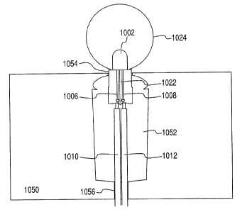
reference to FIG. 20. Molding is performed with mold die 1050 and a
counterpart mold
die (not shown). The mold die 1050 includes a cavity 1052, an upper opening
1054, and
a lower opening 1056. The LED 1000 and the base of cover 1024 are placed on
the mold
CA 02475625 2004-07-23
die 1050 and positioned so that the end portions of the electrical wires 1010
and 1012, the
exposed portions of the contacts i 006 and 1008, the connectors 1014 and 1016,
and the
contact separator 1022 are disposed in the mold cavity 1052. The lens 1004
extends
through the upper opening 1054 of the mold die 1050 to situate the lens 1002
outside the
mold die 1050. Likewise, the majority of the light transmissive cover 1024 is
situated
outside of the mold die 1050. The electrical wires 1010 and 1012 extend
through the
lower opening 1056 of the mold die 1050.
The mold process and techniques will now be described: Vertical injection
molding equipment is preferred as the easiest and most efficient for machine
operators to
align the assembled LED lens, contact wire, and light transmissive cover base
inside the.
injection mold cavity (cavities).
Critical to this waterproof, molded process is selecting a molding temperature
compatible with LED lens encapsulating material. LED lenses 1002 are normally
formed
using an optical grade epoxy. The encapsulating epoxy properties will vary
between
l 5 manufacturers. Further variations in epoxy material are found when flame
retardant
compounds are added to the epoxy. At certain temperature thresholds epoxy
material
will begin to soften, transitioning back into liquid form. This is known in
the art as TG,
or Glass Transition temperature. Exceeding the TG temperature of the LED epoxy
material during the molding, or jacketing process will soften the LED lens
material,
damaging the internal structure of the LED lamp. This is particularly true of
this
jacketing, or molding process as heat from molding is first conducted by the
LED
contacts (1006 and 1008). This causes softening of the epoxy surrounding_the
LED "wire
CA 02475625 2004-07-23
bond" (electrical connection inside the LED lamp completing the circuit from
the LED ,
chip to~the wire frame or contacts) and causing disruption of wire bond
contact.
Mold temperature is not of concern when jacketing, or "over-molding"
conventional, incandescent lamps as the melting point of th.e glass "bulb"
material is
considerably higher than that of the jacketing plastic material.
For j acketing, or over-molding LED lamps one first determines the TG
temperature of the encapsulating epoxy used. Second, the mold temperature and
duration
of the injection (jacketing) process are adjusted so the TG temperature is not
exceeded.
Pre-warming the injection material (PVC, PP, PS, etc.) in its raw granular, or
pellet form
will greatly assist material flow, reduce air pockets, or voids in the
finished jackets, as
well as reduce molding duration and temperature.
According to another embodiment of the invention, a light string comprising a
plurality of LED assemblies is provided, in which at least one of the LED
assemblies
comprises a jacketed LED assembly. More preferably, a plurality or all of the
LED
assemblies are jacketed. The jacketed LED assemblies may have constructions as
described above and as illustrated in FIGS. 18 and 19.
In the event that LED assemblies of a light string are to be individually
jacketed,
the jacketing process may be conducted simultaneously on two or more LED
assemblies
by use of a corresponding number of molds, or one or more molds containing
multiple
cavities for simultaneous jacketing of multiple LED lamp and contact wire
assemblies.
Concurrent practice of this molding technique will improve process efficiency.
The jacketed LED assembly of this invention may be used in various systems and
light strings. Preferred light string systems with which the j acketed LED
assembly of
CA 02475625 2004-07-23
aspects of this invention may be used are described in detail below. It should
be
understood that the following description and attached drawings of preferred
devices,
apparatuses, assemblies, methods, and the like are exemplary, but not
exhaustive as to the
scope of environments in which the jacketed LED assemblies and light strings
of the
present invention may be used.
The term "alternating current voltage", sometimes abbreviated as
°'VAC", as used
herein occasionally refers to a numerical amount of volts, for example, "220
VAC". It is
to be understood that the stated number of alternating current volts is the
nominal voltage
which cycles continuously in forward and reverse bias and that the actual
instantaneous
voltage at a given point in time can differ from the nominal voltage number.
In accordance with an embodiment of the present invention, an LED light string
employs a plurality of LEDs wired in series-parallel form, containing at least
one series .
block of multiple LEDs. The series block size is determined bythe ratio of the
standard
input voltage (e.g., either 110 VAC or 220 VAC) to the drive voltages) of the
LEDs to
be employed (e:g., 2 VAC). Further, multiple series blocks, if employed, are
each of the
same LED configuration (same number and kinds of LEDs), and are wired together
along
the string in parallel. LEDs of the light string may comprise either a single
color LED or
an LED including multiple sub-dies each of a different color. The LED lenses
may be of
any shape, and may be clear, clear-color, or diffuse-color. Moreover, each LED
may
have internal circuitry to provide for intermittent on-off blinking and/or
intermittent LED
sub-die color changes. Individual LEDs of the light string may be arranged
continuously
(using the same color), or periodically (using multiple, alternating CIP
colors), or pseudo-
randomly (any order of multiple colors). The LED light string may provide an
electrical
CA 02475625 2004-07-23
interface to couple multiple light strings together in parallel, and
physically from end to
end. Fiber optic bundles or strands may also be coupled to individual LEDs to
diffuse
LED light output in a predetermined manner.
An LED light string of embodiments of the present invention may have the
following advantages. The LED light string may last far longer and require
less power
consumption than light strings of incandescent. lamps, and the light string
may be safer to
operate since less heat is generated. The LED light string may have reduced
cost of
manufacture by employing series-parallel blocks to allow operation directly
from a
standard household 110 VAC or 220 VAC source, either without any additional
circuitry
(AC drive), or with only minimal circuitry (DC drive). In addition, the LED
light string
may allow multiple strings to be conveniently connected together, using
standard 110
VAC or 220 VAC plugs and sockets, desirably from end-to-end.
Direct AC drive of LED light string avoids any power conversion circuitry and
additional wires; both of these items add cost to the light string. The
additional wires
I 5 impose additional mechanical constraint and they may also detract
aesthetically from the
decorative string. However, direct AC dive results .in pulsed lighting.
Although this
pulsed lighting cannot be seen at typical AC drive frequencies (e.g. 50 or 60
Hz), the
pulsing apparently may not be the most efficient use of each LED device
because less
overall light is produced than if the LEDs were continuously driven using DC.
However,
this effect may be compensated for by using higher LED current during each
pulse,
depending on the pulse duty factor. During "off ' times, the LED has time to
cool. It is
shown that this method ca.n actually result in a higher efficiency than DC
drive;
depending on the choice of AC current.
CA 02475625 2004-07-23
FIG. 1 shows the embodiment of an LED light string in accordance with the
present ;
invention, and as preferred primarily through AC drive. In FIG. 1, the two
block
diagrams correspond to an exemplary string employing I00 LEDs, for either 110
VAC
(top diagram) or 220 VAC (bottom diagram} standard household current input
(e.g., 50 or
60 Hz). In the top block diagram of FICA. lA, the input electrical interface
consists
merely of a standard 110 VAC household plug 101 attached to a pair of drive
wires.
With the average LED drive voltage assumed to be approximately 2.2 VAC in FIG.
lA, the basic series block size for the top block diagram, corresponding to
110 VAC
input, is approximately 50 LEDs. Thus, for the 110 VAC version, two series
blocks of 50
LEDs 102 are coupled in parallel to the drive wires along the light string.
The two drive
wires for the 110 VAC light string terminate in a standard I 10 VAC household
socket
103 to enable multiple strings to be connected in parallel electrically from
end-to-end.
In the bottom block dia~.ram of FIG. 1B, the input electrical interface
likewise
consists of a standard 220 VAC household plug 104 attached to a pair of drive
wires.
With again the average LED drive voltage assumed to be approximately 2:2 VAC
in FIG.
IB, the basic series block size for the bottom diagram, corresponding to 220
VAC input,
is 100 LEDs. Thus, for the 220 VAC version, only one series block of 100 LEDs
105 is
coupled to the drive wires along the light string: The two drive wires for the
220 VAC
light string terminate in a standaxd 220 VAC. household socket 106 to enable
multiple
strings to be connected in parallel from end-to-end. Note that for either the
I 10 VAC or
the 220 VAC light string, the standard plug and socket employed in the string
varies in -
accordance to the country in which the light string is intended to be used.
CA 02475625 2004-07-23
Whenever AC drive is used and two or more series are incorporated in the light
string, the series blocks may each be dri«en by either the positive or
negative half of the
AC voltage cycle. The only requirement of this embodiment is that; in each
series block,
the LEDs are wired with the same polarity; however the series block itself,
since driven
S in parallel with the other series blocks, may be wired in either direction,
using either the
positive or the negative half of the symmetric AC electrical power cycle.
Figures 2A and 2B show two schematic diagram implementations of the top
diagram of FIG. lA, where the simplest example of AC drive is shown that uses
two
series blocks of 50 LEDs, connected in parallel and powered by 110 VAC. In the
top
schematic diagram of FIG. 2A both of these LED series blocks are wired in
parallel with
the polarity of both blocks in the same direction (or, equivalently, if both
blocks were
reversed). With this block alignment, both series blocks flash on
simultaneously, using
electrical power from the positive (or negative, if both blocks were reversed)
portion of
the symmetric AC power cycle: A possible advantage of this configuration is
that, since
the LEDs all flash on together at the cycle rate (60 Hz for this example),
when the light
string flashes on periodically, it is as bright as possible.
The disadvantage of this configuration is that, since both blocks flash on
simultaneously, they both draw power at the same time, and the maximum current
draw
during this time is as large as possible. However, when each flash occurs, at
the cycle
rate, the amount of light flashed is maximal. The flash rate, at 50-60 Hz,
cannot be seen
directly by human eye and is instead integrated into a continuous light
stream.
CA 02475625 2004-07-23
The bottom schematic diagram FIG. 2B shows the alternative implementation for
the tops diagram ofFIG. lA, where again, two series blocks of SO.LEDS are
connected in
parallel and powered by 11Q VAC.
In this alignment, the two series blocks are reversed, relative to each other,
in
polarity with respect to the input AC power. Thus, the two blocks: flash
alternatively,
with one block flashing on during the negative portion of each AC cycle. The
symmetry,
or "sine-wave" nature of AC allows this possibility. The advantage is that,
since each
block flashes alternatively, drawing power during opposite phases of the AC
power, the
maximum current draw during each flash is only half of that previously (i.e.;
compared
when both blocks flash simultaneously). However, when each flash occurs, at
twice the
cycle rate here, .the amount of light flashed is reduced (i.e., half the light
than if two
blocks were flashing at once as previously illustrated): The flash rate, at
100-120 Hz,
cannot be seen directly by the human eye and is instead integrated into a
continuous light
stream.
The trade-off between reversing series blocks when two or more exist in an AC
driven circuit is influenced primarily by the desire to minimize peak current
draw. A
secondary influence has to do with the properties of the human eye in
integrating periodic
light flashes. It is well known that the human eye is extremely efficient in
integrating
light pulses rapid enough to appear continuous. Therefore, the second form.of
the light
string is preferred from a power draw standpoint because the effect on human
perception
is insignificant:
For AC drive with non-standard input (e.g., three-phase AC) the series blocks
may
similarly be arranged in polarity to divide power among the individual cycles
of the
CA 02475625 2004-07-23
multiple phase AC. This may result in multiple polarities employed for the LED
series ,
blocks, say three polarities for each of the three positive or negative
cycles.
As an alternative preference to AC drive, FIG. 3 shows two block diagrams that
correspond to an exemplary string employing 100 LEDs and DC drive, for either
110
S VAC (top diagram.) or 220 VAC (bottom diagram) standard household current
input (e.g.,
SO or.60 Hz). In the top block diagram of FIG. 3A, the input electrical
interface consists
of a standard 110 VAC household plug 301 attached to a pair of drive wires,
followed by
an AC-to-DC converter circuit 302. As in FIG. 1, with the average LED drive
voltage
assumed to be approximately 2.2 VAC in FIG. 3A, the basic series block size
for the top
block diagram, corresponding to l I0 VAC input, is approximately SO LEDs.
Thus, for
the 110 VAC version, two series blocks of SO LEDs 303 are coupled in parallel
to the
output of the AC-to-DC converter 302 using additional feed wires along the
light string.
The two drive wires for the 1 ZO VAC light string terminate in a standard 110
VAC
household socket 304 to enable multiple strings to be connected in parallel.
electrically
1 S from end-to-end.
In the bottom block diagram of FIG. 3B, the input electrical interface
likewise
consists of a standard 220 VAC household plug 30S attached to a paiz; of drive
wires,
followed by an AC-to-DC converter circuit 306. With again the average LED
drive
voltage assumed to be approximately 2.2. VAC in FIG. 3B, the basic series
block size for
the bottom diagram, corresponding to 220 VAC input, is 100 LEDs. Thus, for the
220
VAC version, only one series block of 100 LEDs 307 is coupled to the output of
the AC-
to-DC converter 306 using additional feed wires along the light string. The
two drive
wires for the 220 VAC light string terminate in a standard 220 VAC household
socket
CA 02475625 2004-07-23
308 to enable multiple strings to be connected in parallel from end-to-end.
Note that for
either the I 10 VAC or the 220 VAC light string, the standard plug and socket
employed
in the string varies in accordance to the country in which the light string is
intended to be
used.
FIG. 4 shows an example schematic electrical diagrarrx for the AC-to-DC
converter
employed in both diagrams of FIG. 3. The AC input to the circuit in FIG. 1 is
indicated
by the symbol for an AC source 40I . A varistor 402 or similar fusing device
may
optionally be used to ensure that voltage is limited during large power
surges. The actual
AC to DC rectification is performed by use of a full-wave bridge rectifier
403. This
bridge rectifier 403 results in a rippled DC current and therefore serves as
an example
circuit only. A different rectification scheme may be employed, depending on
cost
considerations. For example, one or more capacitors or inductors may be added
to reduce
ripple at only minor cost increase. Because of the many possibilities, and
because of
their insignificance, these and similar additional circuit features have been
purposely
I5 omitted from FIG. 4.
For either the 1 I O VAC or the 220 VAC version of the LED light string, and
whether or not an AC to-DC power converter is used, the anal manufacturing may
be a
variation of either the basic "straight" string form or the basic
"curtain'° string form, as
shown in the top and bottom pictorial diagrams in FIGS. 5A and 5B. In the
basic
"straight" form of the light string, the standard (110 VAC or 220 VAC) plug
501 is
attached to the drive wires which provide power to the LEDs 502 via the series-
parallel -
feeding described previously. The two drive and other feed wires 503 are
twisted
together along the length of the light string for compactness and the LEDs 502
in the
.~_..~~ _ .~..._ . .. _..~~.._ ~,....~
.~",~,.~>.~..~.~~_M,~,~~,~....,>"...,~.~.,x~~,,....~..._.._
.~.w.~....__.._.__.,~_.___~_ ~a.
CA 02475625 2004-07-23
"straight" form are aligned with these twisted wires 503, with the LEDs 502
spaced ,
uniformly along the string length (note drawing is not to scale). The two
drive wires in
the "straight" form of the light string terminate in the standard
(correspondingly, 110
VAC or 220 VAC) socket 504. Typically, the LEDs are spaced uniformly every
four
inches.
In the basic "curtain" form of the light string, as shown pictorially in the
bottom
diagram of FIGS. 5A and 5B, the standard (110 VAC or 220 VAC) plug 501 again
is
attached to the drive wires which provide power to the LEDs 502 via the series-
parallel
feeding described previously. The two drive and other feed wires 503 are again
twisted
together along the length of the light string for compactness. However,
the,feed wires to
the LEDs are now twisted and arranged such that the LEDs are offset from the
light string
axis in small groups (groups of 3 to 5 are shown as an example). The length
ofthese
groups of offset LEDs may remain the same along the string or they may vary in
either a
periodic or pseudo-random fashion.
Within each group of offset LEDs, the LEDs 502 may be spaced uniformly as
shown or they may be spaced nonuniformly, in either a periodic or pseudo-
random
fashion (note drawing is not to scale). The two drive wires in the "curtain"'
form of the
light string also terminate in a standard (correspondingly 110 VAC or 220 VAC)
socket
504. Typically, the LED offset groups are spaced uniformly every six inches
along the
string axis and, within each group, the LEDs are spaced uniformly every four
anehes.
In any above version of the preferred embodiment to the LED light string,
blinking
may be obtained using a number of techniques requiring additional circuitry,
or by simply
replacing one of the LEDs in each series block with a blinking LED. Blinking
LEDs are
_..,...,.. " ,. ~5.".~ ., -..M....... ,~."..~~~u: ~:.q~, ~-.-"rv-.~. .-.K.,~
".~~,.;,, r.~~~,m~~r. -~e~.rsa ..ate. -,~.~.a., - ._.,r.....~.~ -.~ f
_.T.~"...~..."......~.-..,...
CA 02475625 2004-07-23
already available on the market at comparable prices with their continuous
counterparts, ,
and thus the light string may be sold with the necessary (e.g., one or two)
additional
blinkers included in the few extra LEDs.
Typically, the LEDs in the light string will incorporate a lens for wide-angle
viewing. However, it is also possible to attach fiber optic bundles or strands
to the LEDs
to spatially diffuse the LED light in a predetermined way for a desirable
visual effect: In
such case, the LED lens is designed to create a narrow-angle light beam (e.g.,
20 degree
beaxnwidth or less) along its axis, to enable the LED light to flow through
the fiber optics
with high coupling efficiency. An example of the use of fiber optics is shown
in FIG. 6,
where a very lossy fiber optic rod is employed with intention for the fiber
optic rod to
glow like an illuminated "icicle." 1n FIG. 6, the LED 801 and its housing 802
may be
attached to the fiber optic rod 803 using a short piece of tubing 804 that
fits over both the
LED lens and the end of the fiber optic rod (note that the drawing is-not to
scale). An
example design uses a cylindrical LED lens with a narrow-angle end beam, where
the
diameter of the LED lens and the diameter of the fiber optic rod are the same
(e.g., S mxn
or 3116 inches). The fiber optic rod 803 is typically between three to eight
inches in
length and may be either uniform in length throughout the light string, or the
fiber optic
rod length may vary in either a periodic oi- pseudo-random fashion.
Although the fber optic rod 803 in FIG. 6 could be constructed using a variety
of
plastic or glass materials, it may be preferred that the rod is made in either
a rigid form
using clear Acrylic plastic or clear crystal styrene plastic, or in a highly
flexible form -
using highly plasticized Polyvinyl Chloride (PVC). 'These plastics are
preferred for
safety, durability, light transmittance,.and cost reasons: It may be desirable
to add into
-_. . - ..__.. .K .._m ~.. . ..~..... ,. ,. ".~~"..,.~_..w ,~
~"~~~;~~,~~"~.~~,. -..~_-____
I
CA 02475625 2004-07-23
the plastic rod material either air bubbles or other constituents, such as
tiny metallic ,
reflectors, to achieve the designed measure of lossiness for ofd axis glowing
(loss) versus
on-axis light conductance. Moreover, it is likely to be desirable to add UV
inhibiting
chemicals for longer outdoor life, such as a combination of hindered amine
light
stabilizer (HALS) chenucals. The tubing 804 that connects the fiber optic rod
803 to its
LED lens 801 may also made from a variety of materials, and be specified in a
variety of
ways according to opacity, inner diameter, wall thickness, and flexibility.
From safety,
durability, light transmittance, and cost reasons, it may be preferred that
the cannectiori
tubing 804 be a short piece (e.g., I O mm in length) of standard clear
flexible PVC tubing
(containing LTV inhibiting chemicals) whose diameter is such that the tubing
fits snugly
over both the LED lens and the fiber optic rod (e.g., standard wall tubing
with 1/4 inch
outer diameter). An adhesive may. be used to hold this assembly more securely.
The method of determining and calculating the preferred -LED network that
provides stable and functioning operation wilfnow be described.
Many current-limiting designs use a single impedance element in series between
the
LED network and the power supply. Current-saturated transistors are a less
common
method of current limiting. A resistor is often used for the impedance element
due to low
cost, high reliability and ease of manufacture from semiconductors. For pulsed-
DC or
AC power, however, a capacitor or inductor may instead be used for the
impedance
element. With AC power, even though the waveform shape may be changed by
capacitors or inductors, the overall effect of these reactive elements is
basically the same -
as a resistor, in adding constant impedance to the circuit due to the single
AC frequency
involved (e.g., 60 Hz). In any case, the fundamental effect of current-
lirriiting circuitry is
_. __ .._..._ .._~ ...~-~>_~a.~~~,_.~. x~~.~. ~-~_~....~~~~, ~ry. .- ...._
__..rv.._.___..._.H~ ~___.__~. - ___ ._ ._____-____-m..,...~..~..~.
CA 02475625 2004-07-23
to partially linearize or limit fhe highly nonlinear current versus voltage
characteristic
response curve of the diode, as shown in Figure 7 for a single resistor
element.
Figures 8A and 8B show the preferred embodiment of the invention, wherein a
network of diodes, consisting of LEDs, is directly driven by the AC source
without any
S current-limiting circuitry. Figure 8A is a general schematic diagram showing
M series
blocks of LEDs directly connected in parallel to the AC source where, for the
m-th series
block, there are Nm f I _< m <_ M} LEDs directly connected to each other in
series. Also
shown is a reversal of polarity between some series blocks, placing these
blocks in
opposite AC phase, in order to minimize peak current in the overall AC
circuit. Figure
8B is a block diagram of the above schematic, where a combination pluglsocket
is drawn
explicitly to show how multiple devices can be directly connected either on
the same end
or in an end-to-end fashion, without additional power supplywires in between.
This
end-to-end connection feature is particularly convenient for decorative LED
light strings.
The invention in FIGS. 8A and 8B may have additional circuitry, not explicitly
1 S drawn, to perform functions other than current-limiting. For example,
logic circuits may
be added to provide various types of decorative on-off blinking. A full-wave
rectifier
may also be used to obtain higher duty factor for the diodes which, without
the rectifier,
would turn on and off during each AC cycle at an invisibly high rate (e.g., SO
or 60 Hz).
The LEDs themselves may be amixture of any type, including any size, shape,
material,
color or lens. The only vital feature of the diode network is that all diodes
are directly
driven from the AC power source, without any form of current-limiting
circuitry external
to the diode.
CA 02475625 2004-07-23
Tn order to directly drive a network of diodes without current-limiting
circuitry, the
voltage of each series block of diodes must be matched to the input source
voltage. This
voltage matching requirement for direct AC drive places fundamental
restrictions on the
number of diodes on each diode series block, depending on the types of diodes
used. Far
the voltage to be "matched," in each series block, the peak input voltage,
Vpeak, must be
less than or equal to the sum of the maximum diode voltages for each series
block.
Mathematically, let Vpeak be the peak voltage of the input source and let
V,r,ax(n,m) be the
maximum voltage for the n-th diode { 1 _< n _< Nm} of the m-th series block {
I _< m _< M} .
Then, for each m, the peak voltage must bs less than or equal to the m-th
series block
I0 voltage sum,
Vpeak ~ ~n Vmax(n~m) ~ I )
where { 1 S n <_ Nm} in the sum over n. For simpler cases where all Nm diodes
in the m-th
series block are of the same type, each with V",~, then Vpeak 5 Nm Vmax:
The maximum voltage V",~ of each diode is normally defined by the voltage
which produces diode maximum current, Imax~ However, when diodes of different
types
are used in a series block, the series block value of Imax is the minimum of
all individual
diode values for Imax in the series block. Thus, if the m-th series block has
Nm diodes,
with the n-th diode in the m-th series block having maximum current Imax(n,m),
then the
value of lmax for the m-th series block, lmax(m), is determined by the minimum
of these
Nm individual diode values,
lmax(m) = min[I,nax(n~m) ~ { 1 ~ n ~ Nm} ~ ~ (2)
The maximum voltage Vmax of each diode in the m-th series block is thus
defined
as the voltage which produces the m-th series block maximum current lmax(m).
For
_.______.-rn~~:~~c,_ _ .~ ~-~ ~~.~~~::~", ~ , ..~ ,.. ~ ....~ __ _. _._ _ , _
_._.._~._.___._
r
CA 02475625 2004-07-23
simpler cases where alI diodes in a series block are ofthe same type, each
with maximum
current Ir,,ax~ then Im~(m) = Ice.
For AC or any other regularly varying input voltage, there is an additional
requirement to direct drive voltage matching. Here, in a similar way to peak
voltage
above, the average, or RMS, voltage of the source, V,-",s, must also be less
than or equal to
the sum of the average diode voltages, Va,,g, for each series block.
Mathematically, let
V,T"~ be the RMS voltage of the input source and let Va,.g(n,m) be the average
forward
voltage for the n-th diode {1 5 n < Nm~ of the m-th. series block {1 _< m <_
M~. Then; for
each m, the RMS voltage must be.Iess than or equal to the m-th series block
voltage sum,
1 Q V~ ~ ~ Va~ (n m) (3)
n
where f 1 S n <_ Nm} in the sum over n. Fox simpler cases where all Nm diodes
in the m-th
series block are of the same type, each with V,.~,S, then V,:~,S < Nm Va~g.
In a similar way to the peak voltage above, the average voltage of each diode,
Va"g is normally defined by the voltage which produces diode average current,
Ta"g:
However, when diodes of different types are used in a series block, the series
block value
of Ia,,g is the minimum of all individual diode values for Ia"g in the series
block. Thus, if
the m-th series block has Nm diodes, each with average current Ia"g(n,m) then
the value of
Ia"g for the M-th series block, Ia~g(m), is determined by the minimum of these
Nm values,
Ia~g(m) = min[Ia"$(n,m) ~ f 1 ~ n ~ Nm} ]. (4)
The average voltage Va,,g of each diode in the m-th series block is thus
defined as
the voltage which produces the m-th serifs block average current Ia~g(m). For
simpler
cases where all diodes in a series block are of the same type, each with
average current
Ia"g, then Ia"g(m) = Ia"g.
_~...Anm. ~~~., ~..,,.,~~ ,~.~_ ._._.~ ___ _ _. __ _.._.;~_~_~..
CA 02475625 2004-07-23
Note that the term "average", rather than "RMS," is used to distinguish RNIS ,
diode values from RMS input voltage values because diode values are always
positive
(nonnegative) for all positive or negative input voltages considered, so that
diode RMS
values are equal to their simple averages. Note also that in past LED designs,
the
specified DC value for Inom is equated to the average diode value, Ia,,g. LEDs
are always
specified in DC, and the specified DC value for Inom results from a tradeoff
between LED
brightness and LED longevity. In the direct AC drive analysis below, this
tradeoff
between brightness and longevity results in values for Ia,,g that are
generally different than
Inom. The direct AC drive value for Va,,g 1S thus also generally different
than the LED
I O specified DC value VnQm.
LEDs are specified in terms of DC values, Vnom and Inom. For AC power, since
Va"g is an AC quantity and Vnam is a DC quantity, they are fundamentally
different from'
each other: This basic difference between AC and DC values arises from the
nonlinear.
relationship between diode voltage and diode current..Consider AC voltage
input to a
diode as shown for one period in Figure 9, where the peak voltage shown, VPk,
is less
than or equal to the diode maximum voltage, VmaX. For AC voltages below the
diode
voltage threshold, Vth, the current is zero. As the voltage increases above
Vth to its peak
value, Vpk, and then falls back down again, the diode current rises sharply in
a nonlinear
fashion, in accordance to its current versus voltage characteristic response
curve, to a
peak value, Ipk, and then the diode current falls back down again to zero
current in a
symmetric fashion. Since the voltage was chosen such that Vpk <_ Vmax, then
the peak ' -
diode current satisfies Ipk 5 I,1,~. The average diode cuzrent, Ia,,g, is
obtained by
integrating the area under the current spike over one frill period. . .
. ** _ _ ., " ~. _ . ...*... r. ,* ....._ ~ ~...._..,. mm. ~m.* . .M ,~. t.
..~r~n ,.~ ,~f ..~~~.~,~~~~. ~~~ __n, ~..._..m~ ~..-._m .. ..._ .___
._...T..__~_..~.~...~~m....~ ~._T
CA 02475625 2004-07-23
The central problem of AC voltage matching in equations (1) through (4) for ,
direct drive of diodes is to first determine peak AC diode current, I~~ak and
average AC
diode current, Ia,:g, as a function of Vms or, equivalently, the peak AC
voltage
Vp~k = ~2 V,ns. Since the nonlinear relationship for diode current versus
voltage is not
known in closed form, these diode AC current versus input AC voltage
relationships
cannot be obtained in closed form. Moreover, the nonlinear diode AC current
versus
input AC voltage relationships vary for different diode types and materials.
In all cases,
since the diode current versus voltage characteristic curve, near the
practical operating
point Vno,T,, is a convex-increasing function, i.e., its slope is positive and
increases with
voltage, the average diode current ia~g that results from a given RMS value of
AC voltage
is always higher than the diode current that would be achieved for a DC
voltage input
having the same value. Because of this, specified DC values for diode voltage
cannot be
directly.substituted for AC diode voltage values. Instead, the characteristic
diode AC .
current versus input AC voltage relationships must be found for the AC
waveform of
interest.
The characteristic diode AC current versus voltage relationships may be found
by
measuring diode current values Ia,,$ arid Ipeak as a function of RMS voltage,
V",,5, using
variable voltage AC source. A number of alike diodes are used in these
measurements to
obtain good statistics. If different diode types or materials are considered,
then each
measurement procedure is repeated accordingly. Figure 10 shows a typical
measurement
result for average current, la"g, where the diode used has specified nominal
values of -
Vnom = 2 VDC and Inom = 20 mA.
CA 02475625 2004-07-23
The average AC current curve is always to left of the DC current curve in
Figure ;
10. Thus, Figure 10 shows that if one used DC voltages for the diode in an AC
circuit,
the resulting average AC diode current would be much higher than the DC
current
expected. Recall that in the prior art, where a number of alike 2 VDC LEDs are
, connected in series with a current-limiting resistor, a maximum number N of
LEDs is
defined by summing the individual LED voltages and equating to the RMS input
voltage.
For a 120 VAC source, this maximum number is N = 60 LEDs. The prior art then
subtracts five or ten LEDs from this maximum to obtain a design number, and
computes
the resistor value using the difference between the AC input RMS voltage and
the sum of
these DC LED voltages. This design is marginally stable, and then becomes
unstable, as
the number of LEDs subtracted becomes smaller. Instability is proven in Figure
10, by
considering the limit case where a maximum number N = 60 of LEDs are used and
hence
no LEDs are subtracted. In this limit case, one might argue that a resistor
must be used
anyway, but according to this design formula, presented for five or ten LEDs
subtracted;
the resistor value in this case would equal zero. As Figure 10 shows, if the
resistor value
were zero, i.e:, the resistor is omitted, instead of the DC design value of
Inom = 20 mA for
LED current (the rightmost, DC, curve at 2.0 VDC), the LED average AC current
will be
off the scale, higher than the maximum diode current I~ = 100 mA (the
leftmost, AC,
curve at 1.87 VAC), and the device will fail immediately or almost
immediately.
In order to properly perform matching in an direct AC drive design, the
characteristic diode AC cuirent versus input AC voltage relationships must be
measured - -
and used to specify the AC ,values for equations (1) through (4). DC
specifications and
DC diode measurements cannot directly be used in the direct AC drive design,
and they
CA 02475625 2004-07-23
are useful only as a guide for theoretical inference, discussed further below.
Along with .
the diode average AC current, the diode peak AC current must also be measured
as ,a
function of RMS (or equivalently, peak) input AC voltage. Figure 11 shows a
typical
measurement result, where the diode used has specified DC nominal values of .
S Vnom = 2 ~C arid I"om = 20 mA.
As stated previously, for an AC design, the LED average AC current, Ia,,g, is
generally different from the specified LED nominal DC current, I"om. Likewise,
the LED
maximum AC current, I~, is also generally different from the specified LED
maximum
DC current. Choice of these values represent a tradeoff between LED brightness
and
l 0 electrical efficiency versus LED longevity. In general for pulsed-DC or AC
input, the
LED is off at least part of the time and is therefore has time to cool during
off time while
heating during on-time. In order to increase light output and hence electrical
efficiency,
both the average and the peak diode current values can be raised somewhat
above
specified DC values and maintain the same longevity, which is defined as the
total on-
15 time until; say, 30% loss of light output is incurred - typically at about
100;000 on-time
hours. Moreover, these LED average and peak current values can be raised
further to
increase light output and electrical efficiency at some expense in LED
longevity,
depending on the on-time duty factor. Higher ambient temperatures are
accounted for by
lowering, or "derating" these values somewhat.
20 In a publication by Hewlett Packard, a number of curves are presented of
projected long term light output degradation, for various pulsed-DC duty
factors and
various average and peak current values, at ambient temperature TA =
SS° C. The
AlInGaP LEDs used in this data represents the material commonly used in an LED
with
32
CA 02475625 2004-07-23
specified DC nominal voltage Vnom = 2 VDC. While results vary somewhat for
other
LED materials; it can be inferred from this data that, for most LEDs specified
at
I"om = 20 mA,. the AC design choice for IaVg is approximately in the interval,
30mA<_Ia~g_SOmA (5)
where the specif c value chosen, Ia~g = 36 mA, is indicated in Figure 13.
Similarly, from the Hewlett Packard data it can be inferred that, for most
LEDs
with maximum DC current specified at I00 mA, and the AC design choice for I~
is
approximately,
I~ <_ 120 mA (6)
where a specific value chosen of Imp = 95 mA satisfying this, that corresponds
to
Va~g =1.6 VAC and Ia"g = 36 mA, is also indicated in Figure I I.
To clarify the direct AC drive design, consider again the simpler case where
all N
LEDs in a series block are of the same type, with each LED specified as before
at
Vnom = 2 VDC and I"om = 20 mA. Moreover, let the input AC power be the U.S.
standard
value and assume V~ = 120 VAC for voltage matching. With the above values for
I,t,
and Ia"g, the maximum and average LED voltages, V",~ and Va,,g, are determined
using
AC current versus voltage measurements in Figure 11 and simplified versions of
equations (2) and (4), respectively. The minimum number N of LEDs is
determined from
these voltages using the input voltage Vpeax=~2 VL",s and equations (1) and
(3), for
maximum and average voltage respectively. Since the value for Imp -- 95 mA was
chosen
as a lower value than possible by equation (6), corresponding to Va"g = I .6
VAC and
Ia~g = 36 mA, the maximum voltage becomes VmaX= ~2 Va,,~ and equation (1) is
CA 02475625 2004-07-23
automatically satisfied by satisfying equation (3). Solving equation (3)
results in the ,
minimum number of N LEDs as,
V~ _< N Va"g ~ 120 < N (1.6) ~ N >_ 75 (7)
Although the value of N = 75 is a convenient number to use for manufacturing
S and sale of a decorative LED light string, if a different, less convenient,
nunimum
number N of LEDs were computed, the result can be rounded up or down slightly
for
convenience, provided that the subsequent changes in LED brightness or
longevity are
acceptable. For example, if the RMS voltage were assumed to be 1 I O VAC, then
the
resulting minimum number of LEDs in equation (7) would be N >_ 69, and this
value may
be rounded to a final value of N = 70 for convenience, with only slight impact
on LED
brightness.
Efficiency of the above direct AC drive design example can be estimated by
fiist
noting that the average power, PaVg; consumed by a single LED in the series
block is the
product of the average voltage and the average current, Pa,,g = Va,,g Ia~g.
This is compared
against the optimal DC baseline that uses the specified DC nominal LED power
consumption, Pnom, defined as the product of the nominal voltage and the
nominal
current, P"om = V"°m lnom- Using the values given in the above direct
AC drive example,
there results, Pa"g ~ 1.44 P"°m, so that the direct AC drive design
consumes 44% more
power per LED than the DC baseline. However, to examine efficiency, first let
La,;g be
the average light output power for the direct AC drive design and LDC be the
optimal light - .
output power using the DC baseline. This light output power L represents LED
efficiency as a device, i.e., how much light the LED can be made to produce.
Defining
relative device efficiency as the quotient sD -- Lag / L~ enables the amount
of light
34
CA 02475625 2004-07-23
produced by each LED in direct AC drive design to be compared with the optimal
DC
baseline. Using an approximation that the LED light output power, L, is
proportional to
the LED current, I, this LED device efficiency, so, is approximately,
sD = Lag / LDC ~ Ia~~ / Inor~, = 36 / 20 = 1.8 (8)
so that the direct AC design example makes about 80% more use of each LED as a
light
producing device than the optimal DC baseline. In other words, for each LED
used, the
direct AC drive design produces about 80% more light than the maximum possible
by a
DC design based on nominal LED values. Although this factor of 80% light
increase
appears to be large, its effect is diminished by human perception. According
to the well
I0 known law by Stevens, human perceptions follow a continuum given by the
power
relationship,
B oc L (9)
where L is the stimulus power, B is the perceived brightness intensity, and
exponent p is
a parameter that depends on the type of stimulus. For light stimuli, L is the
light power in
Watts, B is the perceived photopic brightness in lumens, and the exponent is
approximately p ~ 1/3. With this exponent, the 80% increase in light output
power
offered by the direct AC design example translates into about 22% increase in
perceived
brightness. Although a smaller realized effect, the direct AC design example
does offer
an increase, rather than a decrease, in brightness relative to the optimal DC
baseline.
LED electrical efficiency, E, is defined by dividing light output power by
electrical power used, E = L I P. Defining relative electrical efficiency as
the quotient
sE = Ea,,g / EDC enables the electrical efficiency in direct AC drive design
to be compared
"""... , , ~.. ...,. " .m- ,.""., m~ ....n. .,..~o~..x:-~wM,.;-.~-
~~,cc;.~::~sc.N,saux~ss ., a,~. -x ,.,....,~a..,...r....-".. ",.,..-,.~.."...,-
.«»...._...."..,....... _....__.,_..._.._
_._..".r.~,".",..,~.","","w",.,~..".".,......_._.
s~n~waa&,Fa-~m~
CA 02475625 2004-07-23
with the optimal DC baseline. Using again an approximation that the LED light
output ,
power, ~L, is proportional to the LED current, I, there follows,
EE ~ (Iavg / Pavg) / (Inom / Pnom) = unom / Vavg = 2.0 / 1.6 = 1.25 (1.0)
so that the AC direct drive design is about 25% more electrically efficient
than the
S optimal DC baseline. In other words, for a fixed amount of input power, the
direct AC
design examples produces about 25% more light than the maximum possible by DC
based on nominal LED values.
There are two basic reasons for the results iri equations (8) and (I O).
First, the
direct drive design does not have current-limiting circuitry to consume power.
If this
were the only factor involved, the direct AC design efficiency would be I00%,
relative to
the optimal DC baseline, because the optimal DC baseline is computed without
current-
2imiting circuitry loss. The second basic reason stems from the nonlinear
relationship
between LED current and voltage. Because this relationship is a convex-
increasing
function, i.e., its slope is positive and increases with voltage, average AC
diode current
Ia"g is always higher than DC current for the same voltage value, This higher
AC average
current in turn leads to higher average light output, with an approximation
showing a
proportional relationship. This is a fundamental advantage to the pulsed
waveforms over
DC that others fail to recognize for AC and instead try to avoid. The
nonlinear current
versus voltage relationship is further taken advantage of in the direct AC
drive design by
increasing the average current to a more optimal value, using the fact that
the LED has
time to cool during the off time interval ~.n each AC cycle.
An approximation that LED light output is proportional to LED current is very
close for most operating values of LED current, but the approximation usually
CA 02475625 2004-07-23
overestimates light output at high current values. A typical curve for AIInGaP
LEDs, the
common material type for LEDs with a 2 VDC specification, is shown in Figure
12.
With this measured result, the relative direct AC drive efficiencies computed
in equations
(8) and (10) are lowered somewhat, but they are still well above unity. A
numerical
integration using Figure 12 indicates that equations (8) and (10) overestimate
efficiency
of the direct AC design in the example presented by about 15%, and closer
estimates for
the above relative efficiencies are cD ~ 1.53 and EE ~ 1.06.
Diminishing light output power at high LED current places the optimal value
for
RMS and peak LED current values, ra"g and Im~, at a slightly lower value than
the
average and peak current constraints in equations (S) and (6) allow. For
example, Figure
l l shows that.the largest value allowed by equations (5) and (6.) for Va"g is
1.65 VAC,
rather than the value of 1.60 VAC used above.. This larger value of Va"g=1.65
VAC,
achieved by N = 72 LEDs in a 120 VAC series block, is slightly less efficient,
as well as
slightly less reliable, than the value of Va~g,=1.60 VAC and N = 75 LEDs.
However, the
value of N = 72 LEDs in the series block would cost less to produce per unit.
Using 110
VAC instead of 120 VAC to obtain a lower number N = 69 LEDs in the series
block
yields yet slightly lower efficiency and reliability still. For decorative LED
light strings,
this final direct AC drive tradeoff between, say, 70 versus 75 LEDs in the
series block
exemplified is a matter of practical judgment to provide the highest quality
product at the
lowest unit cost.
Although it has been shown above that LED specified DC values cannotbe.
directly used in for direct AC drive, these values do have some theoretical
utility for
using a smaller measurement set to estimate the AC design values. The
theoretical basis
CA 02475625 2004-07-23
of this estimation procedure results from applying statistical inference on
the LED
specifications, using these specifications in a different way than they are
obtained or
intended.
LEDs are specified by two voltage parameters, a typical, or "nominal" voltage,
Vnom, and a largest, or "suprernum" (usually called "maximum" by LED
manufacturers)
voltage, VS"p. These specif canons are obtained as ensemble estimates, for a
large
ensemble of alike LEDs, of "typical" and "largest" DC voltages to expect, from
variations due to manufacturing, that produce the chosen nominal value of DC
current,
Inom. The nominal DC voltage, Vnom, is intended as a "typical" value for the
LED,
obtained either by averaging measurements or by taking the most likely, or
modal, value
in a measurement histogram. The maximal DC voltage, Vsup, is intended as a
largest, or
"supremum," value for the LED, obtained by sorting the largest voltage value
measured
that produces the chosen nominal value of DC current, Inam-
The theoretical problem of interest is to obtain values for average AC
voltage,
Va,,g, and rnaxirnum AC voltage, V'I"~, trat produce average AC current, Ia"g
and
maximum AC current, Imax, respectively. These voltage values Va"~ and Vm~ do
not
consider LED ensemble variations due to manufacturing but instead rely on a
large
enough number N of LEDs in each AC series block for manufacturing variations
to be
averaged over. Otherwise, voltage equations (1) and (3) above must be altered
slightly to
account for expected LED manufacturing variations. Such an alteration would
rely on a
statistical model obtained by measuring variations of the characteristic AC
current versus
AC voltage curve, from LED to LED in a large ensemble of alike LEDs. In any
event,
the voltages V$~g and V~ are fundamentally defined to represent characteristic
estimates
CA 02475625 2004-07-23
of voltage for varying values of LED current, obtained by averaging over the
ensemble,
rather than ensemble estimates, using individual LEDs within the ensemble, of
voltages
that produce a fixed, say, nominal, value of LED current.
In order to make theoretical inferences from LED specifications, it must be
assumed that the specified ensemble random variables representing "nominal"
and
"supremum" voltages can be interchanged with equivalent characteristic random
variables representing corresponding voltages that produce corresponding LED
current
over time. This assumption is similar to a commonly assumed form of ergodicity
in
random process theory that interchanges ensemble random variables with
corresponding
time-series random variables.
With this ergodicity assumption, the AC average and maximum voltage values of
interest, Va"g and V~; can be inferred from the specified diode values for DC
nominal
and.maximum voltage, V"on, and VS"p, respectively, using appropriate DC-to-AC
scaling
between them. It is desired to obtain a single scale factor a for all LED
materials, colors,
and LED manufacturers. In trying to find this single value for scale factor a;
difficulty
arises in that the specified voltages, Vnom and Vsup, are fundamentally
different for
different LED dopant materials. However, given a specific LED dopant material
"M",
such as AIInGaP or GaAIAs, the variations in V"om and VS"~; across applicable
colors and
manufacturers are small enough to be considered fairly insignificant.
Recall that Vmax is equated with peak input voltage Vpeax in equation (1), and
Va,;g _ ..
is equated with RMS input voltage V~ in equation (3). For AC power, the
quotient -
Vpeak I v~ _ ~2. It would thus be desirable if the quotient VS"p I V"om were
also always
a constant; preferably equal to ~2, so that a single scale factor aM could be
used for each
_~.~.___
CA 02475625 2004-07-23
LED material, "M." Unfortunately, this ratio also varies significantly for
different LED ,
materials. As a result, two distinct scale factors aM and ~3M are required for
each LED
material composition, "M." With these material-dependent scale factors, aM and
~iM, the
AC voltages of interests are estimated from DC specified values using,
$ Vavg ~ aM Vnom~ Vmax ~ ~M Vsup~ (11)
where the scale factors aM and j3M are determined by measurement. The
advantage
provided by this theoretical estimation procedure is that the set of
measurements
determining characteristic curves for peak and average AC current versus AC
voltage
need only be obtained for each LED dopant material, independent of LED color
and LED
manufacturer. Of course, the disadvantage to this procedure is that it is
approximate
when compared to making full measurement sets for alI specific types of LEDs
considered, and hence some experimentation with the exact number of LEDs is
required.
For AIInGaP LEDs, Vnom = 2.0 VDC and Vs~p = 2.4 VDC represent the centroids
of specified values across applicable colors and from various manufacturers.
The
characteristic curves presented in Figure 7 were obtained from AIInGaP LEDs.
From
Figure 1 l, and the criteria for average and maximum AC current defined in
equations (S)
and (6), respectively, AC current values Ia,,g = 36 mA and Imp = 95 mA were
chosen
previously, with V,r,ax = '~2 Va"g and Va,,g = l .b VAC. Equations (11), then,
lead to
aAlInGaP = 0.g0 and (3AI~G~ = 0.94. These values may be used theoretically in
equations
(11) to estimate approximate AC average and maximum voltages, Va"g and Vm~,
for - w
other AlInGaP LEDs:
Figure 13 shows measured characteristic curves for a different set of alike
LEDs,
where the dopant material is GaAlAs, rather than AlInGaP. For GaAlAs LEDs,
M .,.~. . ,**. . .* ~ ..,.,~ __ .~,~2~ . ,. _2~.~,*,f~,,~~~-_ ..~,.~__..._..._
__ ... __ .....__. _ _ ._ _ .. ___..____._~._.___._r._
CA 02475625 2004-07-23
Vnom = 1.7 VDC and VS"p --- 2.2 VDC represent the centroids of specified
values across
applicable colors and from various manufacturers. From Figure 13, and the
criteria for
average and maximum AC current defined in equations (5) and (6), respectively,
AC
current values Ia"g = 38 mA and In,aX = 95 mA are chosen, with again Vm~ _ '~2
Va,,g, but
now Va~g = 1.4~ VAC. Equations (11), then, lead t0 CCC,aAIAs = 0.85 and
(3GaAlAs = 0.93.
These values may be used theoretically in equations (11) to estimate
approximate AC
average and maximum voltages, Va"g and Vmax, for other GaAIAs LEDs. Note that,
with
120 VAC assumed for the RMS input voltage, this value Va,,g = 1.45 VAC leads
to
N = 83 LEDs per series block. Similarly, with 110 VAC assumed for the RMS
input
voltage, N = 76 LEDs per series block. Rounding these values Ieads to either
75, 80, or
85 LEDs per series block in a manufactured product, with N = 75 being most
desirable
for a decorative LED light string from a cost basis, if it is sufficiently
reliable.
The above direct AC drive design procedure has been verified by building
numerous decorative LED light string prototypes using a variety of dopant
materials,
colors, and manufacturers. Many of these prototypes were built as long as two
years ago,
and all prototypes have remained operating continuously without any sign of
impending
failure. Moreover, a number of these prototypes were subjected to harsh
voltage surge
and voltage spike conditions. Voltage surge conditions were produced using
high power
appliances in the same circuit, all of which failed to produce anything other
than at most
some flickering. In about half of these experiments the voltage surges created
caused
circuit breakers to trip.
Voltage spikes, simulating lightning discharges, were produced by injecting
1000
V, 10 A pulses of up to 10 ms duration and one second apart into a 100 A main
circuit of
CA 02475625 2004-07-23
a small home using a pulse generator and 10 kW power amplifier. The amplifier
was ,
powered from the main electrical input ofan adjacent home. During these tests,
all
decorative LED light string prototypes merely flickered in periodic succession
at one
second intervals. In the meantime during these tests, the protective circuitry
of adj oining
S electronic equipment shut off without any ensuing damage. All these tests
verified
conclusively that the decorative LED light strings were designed to be highly
reliable by
the direct AC drive method, without the use of any current-limit circuitry.
It is to be understood, however, that current-limit circuitry maybe omitted in
accordance with embodiments of the invention, omission of the current-limit
circuitry is
not required. Instead, current-limit circuitry, such as a resistor, may be
included in the
circuit as am independent element or as part of an LED. For example, one or
more LED
in a series of LEDs may be equipped with a known drop-down resistor integrally
formed
as part of the LED:
It will be understood that various changes in the details, materials and
arrangements
1 S of the parts which have been described and illustrated in order to explain
the nature of
this invention may be made by those skilled in the art without departing from
the
principle and scope of the invention as expressed in the following claims.
This application incorporates the following disclosures by reference: U.S.
Patent
No. 6,461,019, U.S. Patent No. 6,072,280; application serial no. 09/378,631
filed August
20, 1999 titled Preferred Embodiment to Led Light String, now abandoned; and
application ser. no. 09/339,616 filed Sun. 24, 1999, titled Preferred
Embodiment to Led
Light String.
CA 02475625 2004-07-23
The foregoing detailed description of the preferred embodiments of the
invention
has been provided for the purpose of explaining the principles of the
invention and its
practical application, thereby enabling others skilled in the art to
understand the invention
for various embodiments and with various modifications as are suited to the
particular
use contemplated. This description is not intended to be exhaustive or to
limit the
invention to the precise embodiments disclosed. Modifications and equivalents
will be
apparent to practitioners skilled in this art and are encompassed within the
spirit and
scope of the appended claims.