Note: Descriptions are shown in the official language in which they were submitted.
CA 02475850 2004-08-10
WO 2004/064210 PCT/US2003/000463
APPARATUS AND METHOD FOR MEASUREMENT OF DYNAMIC LASER
SIGNALS
BACKGROUND
Field of the Invention
1o The present invention relates to a circuit and method used to calibrate and
compensate
for laser performance in systems such as an optical communications linlcs,
medical
diagnostic systems and any other system utilizing lasers: Performance
compensation
. is achieved in a non-invasive manner without disruption of the laser signal
transmission or other operating parameters of the laser.
Description of the Related Art
Market trends demand increased levels of reliability and intelligence in laser
systems.
Particularly, in laser signal transmission there is the need to send
information with
2o reliable optical power signals. Reliability requires the transmitted
signals to maintain
a given signal strength as well as other performance parameters. Lasers
undergo
degradation due to aging, temperature changes, and other effects. This
degradation
causes the signal strength to be reduced resulting in a decrease of signal- to-
noise
ratio, extinction ratio and an increased Bit Error Rate.
Prior art has utilized either analog controllers or mixed analog/digital
controllers as
opposed to the Digital Controller ( 111 ) shown in Figure 1 below in the
detailed
description.
so Challenges with the Measurement process.
In order to properly control the laser Module ( 106), the Digital Controller (
111 )
requires feedback information from light output (107). When the control system
is
operational, obtaining feedback information becomes problematic since the
light
output (107) constantly changes depending an the Drive Signal (100) the system
is
3s transmitting. Thus any attempts to measure the light output (107) will
encounter
errors, which can render the feedback information unusable.
To perform a measurement of the light output (107), the Drive Signal (100)
needs to
be maintained at a axed power level in order for the system to produce a
steady value
40 of the Light Output (107) so that calibration adJustments can be made. This
procedure
disrupts the signal transmission and, because of this, the transmitter cannot
send
information over the optical communications channel while the calibration is
carried
out. Disruption in communication is contrary to the goals of high reliability
and 100%
up time in present systems.
If the Photodiode Sensor (109) is slow relative to the Laser Module (106),
once the
system is transmitting information, the Photodiode Sensor (109) cannot be
effectively
utilized to calibrate the amplitude of the Light Output (107) because the
sensor may
have a slower response than the laser. The Photadiode Sensor (109) operates as
a
CA 02475850 2004-08-10
WO 2004/064210 PCT/US2003/000463
band-limiting filter converting the response to a variety of waveforms as
follows:
An exponential rise and decay of the Photodiode Sensor (109) output is
produced for a serial stream of the Drive Signal (100) comprised of all
ones. For this data sequence, the average of the Photadiode Sensor (109)
will exhibit the highest value;
A Photodiode Sensor (109) output with an average value close to zero
volts will be obtained for a serial stream of the Drive Signal {100)
comprised of all zeros;
The output of the Photodiode Sensor {109) will exhibit an average voltage
to value, which will between the maximum and minimum values described
above depending on a generic sequence of date with mixed values of ones
and zeros.
To carry out a power measurement of the light output (107), the prior art has
utilized
a variety of methods. In one method the process has been as follows.
. The digital input Drive Signal (I00) is disconnected and a peak value of
analog current from the Modulation Current Generator (103) is applied to the
laser;
. The Light Output (107) is measured with an optical power meter.
~ The Photodiode Sensor ( 109) generates a corresponding signal proportional
to
the light output;
. Adjustments are made in the Controller (111) in order to increase the
magnitude of the optical power coming out of the laser to the desired level;
. The adjustments in the Controller ( 111 ) affect the Bias Current Generator
(102) and Modulation Current Generator (103), which in turn affect the
Light Output (107) of the Laser Module (106);
This approach has the disadvantage of requiring disconnection of the laser
control
system ( 114). Disconnection in many systems, such as communications
equipment,
is not acceptable.
The process for another possible solution previously used is as follows:
Produce a circuit to synthesize a high frequency calibration signal;
Inject the calibration signal into the node between the Modulation Current
Generator (103) and the laser module (106);
3s ~ Sense the calibration signal with the Photodiode Sensor (109);
Add a special filter circuit between the photodiode sensor (109) and the
Digital
Controller ( 111 );
Detect the magnitude of the calibration signal with the Digital Controller
(111).
The problem with this solution is that it affects the information transmitted.
This
4o prior art solution has a significant impact on the reliability of
information
transmission because it essentially inserts noise into the transmitted signal.
Furthermore this approach increases complexity and cost due to an additional
calibration signal generator, a calibration signal injection circuit, plus
filter and
detection circuits.
Because of errors in power measurement, transmission systems in prior art
generally
overdrive the laser to account for variations of temperature, aging and other
effects.
This approach significantly reduces the life of the laser.
2
CA 02475850 2004-08-10
WO 2004/064210 PCT/US2003/000463
SUMMARY OF THE INVENTION
The present invention provides a circuit and a method for calibrating the
Light Output
(107) of the laser without affecting the data transmission. This is consistent
with goals
of high reliability because at no time is the data transmission disrupted.
The present system contains a laser output measurement circuit used in a laser
control
system (114). The circuits contain a photodiode sensor (200), sample and hold
arnpli~er (202), IC with synchronizer and delay circuits (206), and an analog
to
to digital converter (204). The circuits measure the laser light output (107)
while the
laser Module (106) transmits signals. The measurement circuit tracks and
stores the
laser light output (107) signal using a Photodiode Sensor (109) and with a
Sample/hold (202). The methods calculate the value of the laser light output
(107)
from mathematical relationships, which correlate the light output (107) of the
laser
is Module (106) to the current value of the drive signal (100). Some of the
distinguishing features in the present invention are 1) feedback information
from the
photodiode is obtained in a synchronous manner as a snapshot of the laser
performance, and 2) the measurements are precise and calibrated, and 3) no
disruption of the signal transmission occurs.
An advantage of this invention is that laser power amplitude can be calibrated
without interrupting the flow of information transmission.
Another advantage of this invention is that the system can utilize multiple
types
of output responses from the Photodiode Sensor with the utilization of the
appropriate
2s correlation algorithm.
Another advantage of this invention is that the transmitter optical power can
be
continuously maintained at the optimal value to achieve the target Extinction
Ratio,
Bit Error Rate and analog signal level.
Another advantage of this invention is that the laser can be compensated for
3o degradation due to aging.
Yet another advantage of this invention is that adjustments to account for
temperature
changes, aging and other effects are done only as needed and by the amount
needed.
This contributes to extending the life of the laser.
BRIEF DESCRIPTION OF THE DRAWINGS
Details of the invention, and of the preferred embodiment thereof, will be
further
understood upon reference to the drawings, wherein closely related elements
have the
4o same number but different alphabetical suffixes, and further wherein:
Fig 1 illustrates a control system diagram for a laser transmitter. This
control system
shows a configuration presented in previous applications of the same inventor.
Fig 2 illustrates a diagram of the Output Signal Sampler.
Fig 3 illustrates an embodiment of the Output Signal Sampler.
4s Fig 4 illustrates the timing diagram for the calibration process.
Fig 5 illustrates a circuit, which can be used to facilitate held calibration.
Fig 6 illustrates the power measurement calibration.
Fig 7 illustrates the factory calibration of the sensor circuit.
3
CA 02475850 2004-08-10
WO 2004/064210 PCT/US2003/000463
DETAILED DESCRIPTION OF THE PREFERRED EMBODI1VIENTS
The above-mentioned difficulties and problems of the prior art are overcome by
the
present invention.
Apparatus
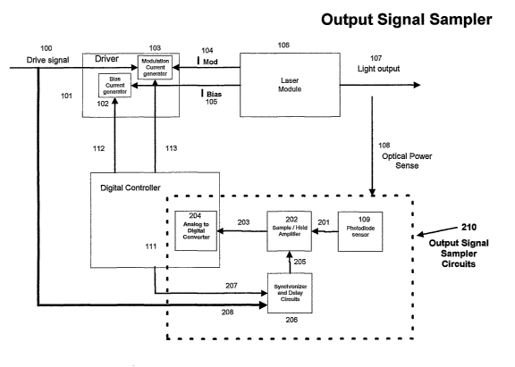
Referring to FIG 1, a block diagram is shown for a Laser Control System (114).
The
to system consists of a drive Signal Input (100) applied to a Laser Module
Driver (101),
which contains a Bias Current Generator (102) and a Modulation Current
Generator
(103). A Bias Control Signal (112) and a Modulation Control Signal (113)
control
the current generators. The Driver ( 101 ) produces Modulation Current ( 104)
and Bias
Current (105) that are applied to the Laser Module (106). The Laser Module
(106) in
is turn produces Light Output (107). The magnitude of the Light Output (107)
bears a
relationship to the magnitude of the Modulation Current (104) and the Bias
Current
(105). A portion of the Light Output (107} from the laser is sensed. This
portion
constitutes the Optical Power Sense (10~), which is coupled to a Photodiode
Sensor
(109). The Photodiode Sensor Output (110) is connected to a Digital Controller
(111).
2o The Digital Controller (111) contains algorithms for laser control and also
determines
the magnitudes of the Bias Current Generator (102) and Modulation Current
(103).
Figure 2 shows the output signal sampler apparatus of this invention. This
consists of
a Photodiode Sensor (109), which generates a Photodiode Signal (201) in
response to
2s the application of a portion of the Laser Light Output (107). The
Photodiode Output
may be a fast response or an exponential rise and decay signal. The Sample and
Hold
Amplifier (202) receives the Photodiode Sensor Signal (201) and stores the
value of
the signal at the appropriate time as directed by the Sample and Hold Control
(205).
Once the Sample and Hold Amplifier (202) has stored the signal, it is sent to
the
3o Analog to Digital Converter (204), which is contained in the Digital
Controller (111).
The Sample and Hold Amplifier (202) is connected to the Analog to Digital
Converter (204).
The Sample and Hold Control (205) is produced by the Synchronizer and Delay
s5 Circuits (206). These circuits utilize real-time information of the state
of the Drive
Signal (100), which connects to the Drive Signal (100) at (20~) in order to
determine
when the Sample and Hold Control (205) is activated. The Synchronizer and
Delay
Circuits (206) are controlled by the Digital Controller (111) with the
necessary Logic
Output (207). The Digital Controller ( 111 ) contains algorithms that are
capable of
4o utilizing a multiplicity of Photodiode Sensor information including an
exponential
rise and decay, a square wave response, and an average signal output. The
algorithms
utilize information related to the sequence of values of the Drive Signal
(100) input
and correlate those values to the magnitude of the Photodiode Sensor (109)
output. In
addition, the controller can then make adjustments to the Bias Current (105)
and
4s Modulation Current (104), in order to optimize the extinction ratio and the
Bit Error
Rate.
4
CA 02475850 2004-08-10
WO 2004/064210 PCT/US2003/000463
Figure 3 is an embodiment of the Output Signal Sampler in this invention. The
Drive
Signal (100) applied to the Driver (103) produces a Light Output (107). A
portion of
the optical power is coupled to the Photodiode Sensor (109). The Photodiode
Sensor
(109) produces a current, which is converted to a voltage by the
Transimpedance
s Amplifier (301). This voltage drives the Sample and Hold Amplifier (302),
which in
turn produces a steady sample of the sensor signal at (304) to the Analog to
Digital
Converter (304). The Sample and Hold Amplifier (202) stores the sensor
information
in a Capacitor CH (316). The capacitor is chosen so that the capturing of the
sensor
signal is done at high speed while at the same time the capacitor maintains
the value
i o of the captured sensor signal during the analog to digital conversion. In
general, for
optical teleconnnunications, the capacitor may need to be relatively small in
the tens
of picofarads in order for the Sample and Hold Amplifier (202) to successfully
track
the sensor signal. The Transimpedance Amplifier (301) and the Sample and Hold
Amplifier (202) are designed in such a way that they will be substantially
faster then
1s the Photodiode Sensor (109) in order to insure that the Photodiode Sensor
(109)
determines the frequency response. A critical feature of the present invention
is the
appropriate timing of the Sample and Hold Control (205). This control must be
able
to captuxe the Photodiode Sensor (109) signal at a predictable time in order
to
anticipate the state of the Drive Signal (100) and the Light Output (107). The
timing
2o synchronization circuit determines this. This circuit starts by sampling
the Drive
Signal (100) at (315). This is done with the use of a Buffer (314) in order to
avoid a
significant load on the Drive Signal ( 100). The output of the Buffer (314) is
sent to a
set of n signal propagation delays. These delays consist of Delay 1 (312) to
Delay n
(313). These delays connect to Digital Multiplexer (309) through Inputs (310)
to
2s (311). The Digital Controller utilizes the Input Select (308) of the
Digital Multiplexer
(309) in order to select any of the n signal propagation delays. A zero to one
transmission of the Drive Signal (100) will cause, after a time delay, a zero
to one
transition at the Set Input (307) of the Set Reset Latch (305). This
transition in turn
causes a zero to one transition of the Sample and Hold Control (205), which
places
3o the Sample and Hold Amplifier (202) in hold mode in order to prepare the
system for.
an analog to digital conversion. After the analog to digital conversion is
completed
the Set Reset Latch (305), is placed in reset mode by the Reset Signal (306)
generated
by the Digital Controller (111). This last step will then place the Sample and
Hold
Amplifier (202) in sample mode so that the system can be ready for the next
3s calibration cycle.
Figure 3 shows the propagation delays associated with the Output Signal
Sampler.
The following definitions apply:
tr Buffer (314) input to output propagation delay
tz= Selected propagation delay.
4.o t3 Digital Multiplexer (309) propagation delay.
t4 Set input to Output propagation delay for Set Reset Latch (305).
is Propagation delay from Sample and Hold Control S/H (408) input to the
opening of the internal switch in the Sample and Hold Amplifier (202).
tD,;~e (414)= Propagation delay across the Driver (103) + time for the Laser
4.s (I06) to switch logic state
tse"Se (406) = Time for the Photodiode Sensor (109) to respond + time for the
Transimpedance Amplifier (301) to respond
tCaP~re (414) = Time for the Sample and Hold Amplifier (202) to track the
photodiode sensor signal.
CA 02475850 2004-08-10
WO 2004/064210 PCT/US2003/000463
tsyn~h (415 = tr + tz + t3 + t4 + t5 . . . . . . . . . . . . . . . . . . . . .
. . . . . . . . . . . . ..Equation 1.
In order to maximize Vpeak (407), the following equation must be satisfied:
tsY"~,,(415)= t~.;~e(414) + tse~e (406) + t~aP~,~(414)
...........................Equation 2.
When the S/H (408) is in hold mode after the transition at 409, the Analog to
Digital
Converter (204) performs an analog to digital conversion, which will last for
a period
of time t,~,D (412). The duration of the analog to digital conversion can be
relatively
slow as required by the Analog to Digital Converter (204). At the end of the
~o conversion, the Digital Controller (111) will cause the S/H (40~) signal to
experience
a Reset (412) transition to the sample mode with the use of the Reset Control
(306).
The embodiment shown in Figure 3 may utilize MOS technology components for a
given data rate of transmission. Synchronization of the timing characteristics
and
delays as indicated by Equation 2 can be best achieved by including the Signal
is Sampler circuits of Figure 3 in the same integrated circuit as the Driver
(103). If a
single integrated circuit is not available, then the Signal Sampler circuits
must be
implemented with the appropriate technology in order to match the speed
requirements of the propagation delays associated with the laser Driver (103).
Very
fast Silicon Germanium and other technologies are available. In some
applications,
2o fine-tuning and modifications of the embodiment of Figure 3 will be
necessary to
keep up with fast transmission rates. In these cases the same principles of
the
invention will apply and the task will consist of selecting the appropriate
configuration of high-speed components.
2s Figure 4 shows the timing of the in line calibration of the laser optical
power. As a
reference to the timing of the system consider the system clock that is
utilized by the
transponder. This is the clock CLK (400). The clock (400) is utilized in the
system to
generate Serial Data Di (401). In this example the Serial Data Di (401)
consists of the
sequence 101. The data transmission of the timing diagram in the illustration
3o corresponds to NRZ-L. After the zero to one transition of the Serial Data
Di at (402),
the data flows through the Driver (103) and causes a zero to one transition in
Laser
Optical Power PL (403). This transition of the Laser Optical Power (403)
happens
after a delay t D,;Ve (413), corresponding to the delay of the signal flowing
through the
Driver (103) and the Laser (106). A given setting of the Bias Current
Generator (102)
ss places the Laser (106) slightly above the threshold. This setting can be
adjusted and
controiler independently from the signal modulation current. For the purpose
of
calibrating the Light Output (107) focus on the control of the Modulation
Current
Generator (103). For the pulse of the Serial Data Di (401), there is a
corresponding
amplitude of the Laser Optical Power Output PL (403). The magnitude of the
optical
o power is noted as Pmax (404). The laser optical power corresponding to the
transmission of a logical 1 will vary depending on the setting ofthe
Modulation
Current Generator (103), the Laser (106) characteristics and the effects of
factors such
as temperature and aging on the Laser (106). The Photodiode Sample Hold
Response
VPs (405) will start sensing the Laser ( 106) output after a delay of t se"se
(406). The
4s Sample and Hold Amplifier (202) will start increasing its voltage in an
exponential
manner reaching a maximum value Vpeak (407). High frequency models have been
determined that demonstrate how the combination of amplifiers and Photodiode
Sensor (109) can respond with an exponential rise and decay characteristic.
Associated circuit components such as resistors and capacitors can be utilized
to
6
CA 02475850 2004-08-10
WO 2004/064210 PCT/US2003/000463
ensure there is a dominant pole response resulting in a controlled exponential
characteristic without signal ringing. There can be high performance circuit
implementations of the laser sensor circuits where the Photodiode sensor
(109),
Transimpedance Amplifier (301) and Sample and Hold Amplifier (202) exhibit a
s response with a bandwidth fast enough to keep up with the laser bandwidth.
In this
case, a rather fast rise and fall signal will result rather than the
exponential rise and
decay. The exponential rise and decay characteristic is illustrated here
because it is
fairly common for laser packages to be available with an integrated low-cost
monitoring photodiode. These integrated packages normally have a monitoring
io photodiode that exhibits a slow frequency response.
After a delay of ts~~n (415) from the zero to one transition of the Serial
Data Di (401 ),
the Sample and Hold Control S/H (408) will experience a transition from Sample
(410) mode to Hold (411) mode at 409. Transition at this point in time ensures
that it
is possible to capture the maximum possible value of Vpeak (407). This will
produce
1 s a higher resolution in our measurement system.
Method of Operation
Signal strength optimization of the Laser power sensor.
The Digital Controller (111), upon power up goes through an initialization
process.
2o Part of the initialization routine consists of a process used to optimize
the sensor
signal. The objective of the process is to maximize the value of Vpeak (407).
Maximizing the value of Vpeak increases the resolution and accuracy of the
laser
power measurement system.
This is accomplished with an iterative process where the Digital Controller
(111) will
2s automatically select the timing delays one at a time and determine which
produces the
highest value of the Vpeak (407). This process can be carried out during the
factory
test of the transmitter. The needed value of the timing delay is then stored
in the
internal memory of the Digital Controller ( 111 ) so it can be used in the
field. The
process can also be carried out in the field with an addition to the circuit
of Figure 3.
This is illustrated in Figure 5. The Controller (111) uses Switch Controls
(502, 503)
to control the switches S 1 (500) and S2 (501 ). When Switch S 1 (500) is
opened, the
Drive Signal (100) is disconnected. At the same time, the switch S2 (501) can
be
closed. This allows the Controller (111) to place a train of pulses into the
Driver
ss (103) in order to calibrate the timing of the Output Signal Sampler and to
calibrate the
Extinction Ratio.
Power sensor measurement calibration.
To carry out continuous laser performance compensation, this invention relies
on
4.o correlating the photodiode sensor signal with the pattern of information
transmitted
over the optical communications link. By capturing and storing the data
pattern
information and the corresponding sensor signal, the controller (111) can
compute the
correlation algorithms. Many algorithms that can accommodate multiple system
responses are possible. One example of the correlation is as follows.
as Consider the exponential rise and decay of the Photodiode Sample Hold
Response
(405). The Digital Controller (111) can allow the charge stored in the
capacitor CH
(316) to decay to zero volts prior to sampling the Laser power output
response. The
response of the Signal Sampler in Figure 3 will be governed by the following
equations:
7
CA 02475850 2004-08-10
WO 2004/064210 PCT/US2003/000463
Exponential rise
V(t)= V",(1-a ~c ) ... ... ... ... ... ... ... ... ... ... ... ... . Equation
3.
Where Vm represents the asymptotic maximum value of the exponential rise
response,
R and C are the equivalent circuit constants and V(t) is the voltage at the
Sample and
Hold Amplifier (202) .
Exponential decay
V(t)= VPe ~c ... ... ... .. . ... ... ... .. . ... ... ... .. . ... . Equation
4.
1o Where Vp represents the maximum value attained during the exponential rise
response as determined by the circuit parameters and the data rate of
transmission, R
and C are the equivalent circuit constants and V(t) is the voltage at the
Sample and
Hold Amplifier (202).
~s Figure 6 shows the power measurement calibration. The following definitions
apply:
PPH~ (600)= Laser power pulse received at the photodiode for a given setting
of laser
power output. This is proportional to the pulse of power that the laser emits
in
response to the logic one transmission.
P~~~1 (604)= Maximum value of Laser power pulse received at the photodiode.
The
magnitude of the photodiode power is determined by the Driver (103), Laser
(106)
and the amount of light coupled from the laser to the photodiode.
V1(t) (601)= Time dependent response of the photodiode(109) output, the
Transimpedance Amplifier (301) and the Sample and Hold Amplifier (202). This
response is the corresponding response to PPHI (600).
Vml (606)= Asymptotic value of the exponential response for V1(t) (601). This
is
3o proportional to PPHMm (604). The proportionality constant is the
Responsivity of the
photodiode.
Vpeakl (605)= Peak value of exponential response corresponding to the end of
the
pulse for the transmission of a logic one.
Similarly, for a different set of conditions, the laser will emit a pulse with
a different
level of power magnitude. The following definitions apply:
PPS (602)= Laser power pulse received at the photodiode for a second setting
of laser
4o power output.
PP~~ (607)= Maximum value of Laser power pulse received at the photodiode.
V2(t) (603)= Time dependent response of the photodiode(109) output, the
a.s Transimpedance Amplifier (301) and the Sample and Hold Amplifier (202).
This
response is the corresponding response to PPS (602).
Vm2 (609)= Asymptotic value of the exponential response for V2(t) (603). This
is
CA 02475850 2004-08-10
WO 2004/064210 PCT/US2003/000463
proportional to PP~~ (607). The proportionality constant is the Responsivity
of the
photodiode.
Vpeak2 (608)= Peak value of exponential response corresponding to the end of
the
pulse for the transmission of a logic one.
Focusing now on the corresponding equations the following relationships are
obtained:
Vpeakl= V",1(1-e -Tmlc~ ) ... ... ... ... ... ... ... ... ... ... ... ... ...
... ... ... ... ..Equation 5.
1o Vpeak2= V"~(1-a -Tlmc~ ) ... ... ... ... ... ... ... ... ... ... ... ...
... ... ... ... ....Equation 6.
Where t has been substituted by T1 for a given value of period for a logic one
transmission, in this case a constant. R1 and C 1 correspondingly have
substituted R,
C since for a given circuit, the parameters are constant.
In general, equations 5 and 6 show how once the period and the circuit RC
parameters
15 are fixed, the quantity (1-a 'Tl/R1C1 ) becomes a constant and the peak
values of the
exponential rise are dependent only on the asymptotic values of the photodiode
response. The asymptotic values bear a linear relationship to the laser output
power.
In this case additional calibration processes need to be considered, which
will control
second order effects of the laser and photodiode transfer function such as
temperature
2o effects.
It is then concluded that the Vpeak (407) of the exponential rise and decay of
the
photodiode sensing circuits will vary linearly would respect to the maximum
amplitude Pmax (404) of the Laser Optical Power Output (403).
25 Factory or field calibration of the sensor circuit is shown in Figure 7.
The amplitude of the sensor signal is first maximized. At 700 apply a
continuous
stream of all 1's to the data input. At 701, while maintaining the stream of
all 1's,
sequence Signal Sampler delays 312 to 313. The delay that produces the
strongest
signal is chosen. At 702, apply a continuous stream of all 0's. At 703,
measure the
3o value of the laser power with an optical power meter. Also an A/D
conversion to
measure the baseline sensor signal for a zero transmission is performed. At
704, then
apply a stream of all 1's. At 705, while measuring power with optical power
meter,
continuously adjust magnitude of laser power by controlling the Modulation
Current
Generator (103) until the maximum possible value of the laser power output is
ss reached. The corresponding sensor output is measured and stored in the
Digital
Controller (111).
The above calibration process can be modified for some applications if the
process
yield characteristics of the laser are understood. In that case, the sensor
can still be
4o calibrated but the process does not rely on the Optical Power Meter to
determine how
much power the laser puts out for all 1's and all 0's. Instead, process
parameters can
be used to coarsely determine the output power for a given setting of the
Modulation
Current Generator (103).
During normal operation, a linear interpolation of the values of the sensor
between
4.s the all 0's value and the all 1's value will determine the measured laser
power output.
These measured values of power output are then utilized to optimize
performance on
a continuous manner while the system is operational.
Extinction Ratio and Bit Error Rate Optimization.
9
CA 02475850 2004-08-10
WO 2004/064210 PCT/US2003/000463
The methods are related to ensuring the optimal value of extinction Ratio and
minimal Bit Error Rate. The firmware imbedded in the Digital Controller (111)
utilizes the results from the A/D conversion of the sensor and proceeds to
make
adjustments to the amplitude of the peak laser power in response to the logic
high
s sent. The laser power for logic high needs to send a signal with a
sufficiently large
value according to the transmission protocol. With the precision power
measurement
circuit of this invention, the laser is not overdriven thus extending
operating life.
The Digital controller (111) makes adjustments to the minimal optical power in
response to the logic low sent and. The minimal optical power is determined by
the
1o Bias Current Generator (102) and is adjusted above the threshold of the
laser. The
current needs to strike a balance between having too low of a value (needed to
maximize extinction ratio) or too high of a value (needed to obtain a margin
over the
lasing threshold and to not operate over the noisy region of the laser near
the
threshold). Since the above adjustments are performed in a continuous manner,
the
1 s laser is always operated at the optimal levels of power output.
Remarks
and comments
on some
advantages
of the
invention
1. A circuit that precisely calibrates the laser optical
power in a continuous
manner without disrupting the flow of information
in the optical
2o communications link.
2. A method that utilizes knowledge of the measured value
of the laser optical
power and makes necessary adjustments to optimize
the values of the
Extinction Ratio and Bit Error Rate.
3. A circuit that can utilize any type of response from
the sensing photodiode.
25 4. A method that utilizes knowledge of the information
sent to the optical
communications link to determine how the laser should
be performing.
5. A circuit and method utilized to compensate for aging,
temperature rise and
other degradation effects of the laser without interrupting
the flow of
information transmitted.
so 6. A circuit and method that compensates for aging, temperature
rise and other
degradation effects of a laser only as needed at any
point in time rather than at
the beginning when power is turned on or at the factory.
7. A process that automatically maximizes the magnitude
of the photodiode
power sensor signal for a laser.
3s ~. A circuit to capture a sense the laser output where
the sensing is coordinated
with the transmission signal.
9. A circuit as in ~, where the associated timing of
the circuit is automatically
optimized.
a.o Consequently, while the foregoing description has described the principle
and
operation of the present invention in accordance with the provisions of the
patent
statutes, it should be understood that the invention may be practiced
otherwise as
illustrated and described above and that various changes in the size, shape,
and
materials, as well as on the details of the illustrated method of operation
may be
4s made, within the scope of the appended claims without departing from the
spirit and
scope of the invention.