Note: Descriptions are shown in the official language in which they were submitted.
CA 02476213 2004-08-12
Securit;r element and security document with such a
security element
[O1] The invention relates to a security element as well as a security
document, in
particular document of value as for example a bank note, with such a security
element.
The invention also relates to a semifinished product for producing such a
security
document. In particular, the invention relates to a security element in the
form of a
security thread for embedding in the security document as a so-called window
thread
and in the form of a label or transfer element for application to the security
document.
[02] Security documents within the terms of the present invention are in
particular
bank notes, but also checks, check cards, credit cards, identity cards,
passports,
admission tickets, tickets for public transport and the like. As semifinished
products
for the production of the aforementioned security document for example
unprinted
security paper and other unprinted security document substrates are suitable.
[03] For protection against imitation and as authentication the aforementioned
security documents are typically equipped by means of embedded security
threads or
applied security labels or security transfer elements. Security threads in the
form of
window threads are widely known, for example, in connection with documents of
value, such as bank notes, but are, in principle, also suitable for the use in
check cards
and the like. Window threads are embedded in the base material of the security
document and appear periodically at the surface of the security document, so
that they
are visually recognizable in these "window areas". In translucent substrates a
so-called
incident lightltransmitted light effect is the result, the security thread
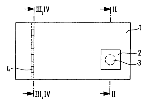
viewed in
transmitted light appearing as a dark stripe vis-a-vis the surrounding
material. In
incident light, however, the security thread is recognizable only in the
window areas.
CA 02476213 2004-08-12
2
[04] One distinguishes between simple window threads which appear only on one
surface and two-sided window threads which appear on both surfaces, one
special case
of two-sided window threads hereinafter being referred to as lookthrough
window
thread which is visible on both sides of the document of value at the same
time. A
lookthrough window thread, so to speak, spans a hole or a transparent area in
the
document of value. A further two-sided window thread is the security thread
referred
to in the following as alternating window thread which is alternately visible
on the
front or the back of a document. Apart from security threads there is also the
possibility for using so-called transfer elements as security elements, these
usually
spanning gaps, for example a hole, in a document.
[OS] The security elements have complex, visually and/or automatically
testable
security features which can only be imitated with great efforts. As to
additionally
increase the protection against forgery, such security elements often have
several
different security features which can also have, when combined, a new common
effect.
[06] One security feature which can often be found in security elements is a
multilayer dichroic coating, whose color effect changes depending on viewing
angle
and/or the viewing in transmitted light or incident light. This phenomenon is
based on
interference effects due to the overlapping of multiple reflections and/or
multiple
transmissions of light waves within the layer structure in combination with
selective
absorption properties of the layer materials. The change of color from varying
viewing
angles is also called color shift effect. The change of color when viewed
alternately in
incident light and in transmitted light, in contrast, is hereinafter referred
to as color
change effect.
[07] Optical interference coatings with color shift effect in connection with
security
elements are described in, for example, EP 0 395 410 B1, EP 0 341 002 B1, WO
O1 / 03945 A1 and US 3,858,977. Depending on kind and number of layers in the
layer
structure 2, 3, 4 or more color effects depending on the viewing angle can
occur. The
reflection and transmission properties of such color shift effect layers
depend on
several factors, in particular on refractive indices, absorption coefficients
and layer
CA 02476213 2004-08-12
3
thicknesses as well as on the number of layers in the layer structure. It is
equally
known to integrate the interference layers in a security element all over or,
however, as
described for example in WO 00 / 31571 A1, to break down into tiny flakes and
to mix
these with printing ink.
[08] Although security elements with dichroic coating have already been
proposed,
there is still a need for security elements improved in contrast to the
already existing
security elements.
[09] It is therefore the problem of the present invention to provide security
elements,
in particular a security thread or a transfer element, which, compared to
prior art, have
an enhanced forgery-proofness.
[10] This problem is solved according to the invention by a security element
as well
as a security document or a semifinished product with the features of the
independent
claims. In claims dependent on these are specified advantageous developments
and
embodiments of the invention.
[11] According to that the multilayer security element has an interferential
layer
structure which produces a color shift effect on both the front as well as the
back of the
security element when the security element is viewed from different angles.
Here the
color shift effect on the front and back of the security element can be
designed in the
same way but also differently.
[12] Due to the complex multilayer structure of the security elements and the
therefore only difficultly reproducible color shift and color change effects,
they can be
imitated only with great effort.
[13] The interferential layer structure here is composed of at least two
multilayer
interference elements (I1, IZ) and at least one reflection layer R.
[14] The interference element is formed by absorber and dielectric layers
located
one on top of the other, wherein also several absorber and dielectric layers
can be
disposed alternately one on top of the other. Instead of alternating absorber
and
CA 02476213 2004-08-12
4
dielectric layers exclusively dielectric layers can be provided, too,
adjoining layers
having strongly different refractive indices so as to produce a color shift
effect. The
use of the absorber layers, however, is advantageous, because the color shift
effect is
visible better.
[15] In principle, the interference elements I1, IZ can be structured in a
multilayer
fashion, but they each comprise preferably at least two layers, namely one
absorber
layer A1 or A2 located on the outer side and one dielectric layer D1 or D2
located
between the respective absorber layer and the inner reflection layer R. As
absorber
layers A1, AZ typically serve metal layers of materials such as chromium,
iron, gold,
aluminum or titanum of a thickness of preferably 4 nm to 20 nm. Compounds such
as
nickel chromium iron or rarer metals such as vanadium, palladium or molybdenum
can
also be used as materials for absorber layers. Further suitable materials are
specified
for example in WO O1 / 03945 A1, e.g. nickel, cobalt, tungsten, niobium,
aluminum,
metal compounds such as metal fluorides, metal oxides, metal sulphides, metal
nitrides, metal carbides, metal phosphides, metal selenides, metal silicides
and
compounds thereof, but also carbon, germanium, cermet, iron oxide and the
like.
(16] The absorber layers AI, A2 of the interference elements can have the same
or
different thicknesses within the interferential layer structure and/or consist
of the same
or different absorber materials.
[17] For the dielectric layer D~, D2 mainly transparent materials with a low
refractive
index <1.7 are considered, such as for example Si02, MgF, SiOx with 1 < x < 2
and
A1203. In principle, nearly all transparent compounds which can be vapor-
deposited
are possible, therefore in particular also higher refracting coating materials
such as
Zr02, ZnS, Ti02 and indium tin oxides (ITO). Further materials suitable for
the
dielectric layers D;, D2 are specified for example in WO O1 / 03945 A1. The
layer
thickness of the dielectric layers D1, DZ is in a range of 100 nm to 1000 nm,
preferably
200 nm to 500 nm.
CA 02476213 2004-08-12
[18] The dielectric layers of the interference elements can have the same or
different
thicknesses within the interferential layer structure and/or consist of the
same or
different dielectric materials.
[19] Preferably the interference elements are designed differently within the
interferential layer structure, so that they each produce different color
shift effects.
[20] Instead of absorber layers A,, A2 also dielectric layers can be used, the
refractive index n of adjoining dielectric layers having to be greatly
different, on the
one hand n <1.7 and on the other hand n > 1.7 so as to cause a distinct color
shift
effect. Since with this structure for a distinct color shift effect several
dielectric layers
are necessary and thus the production is very expensive, the use of absorber
layers is
preferred.
[21] The absorber layers A1, A2 and dielectric layers D~, D2 of the
interference
elements I1, I2 as well as the reflection layer R are preferably produced by
means of a
vacuum vapor deposition method on the substrate S which can form a component
of
the security element 1, but which can also serve only as an intermediate
carrier and is
removed when the security element is applied to or in an object at the latest.
[22] Most different vapor deposition methods are suitable for the production
of the
layers. One methodic group is formed by physical vapor deposition (PVD) with
evaporation boat, vapor deposition by resistance heating, vapor deposition by
induction heating or also electron-beam vapor deposition, sputtering (DC or
AC) and
electric-arc vapor deposition. Furthermore, the vapor deposition can also be
effected
by chemical vapor deposition (CVD) as e.g. sputtering in reactive plasma or
any other
plasma activated vapor deposition method. In principle, there is also the
possibility
that dielectric layers are printed on.
CA 02476213 2004-08-12
6
[23] The reflection layer R is preferably a metal layer for example of
aluminum,
silver, nickel, platinum or palladium, preferably of silver or aluminum or of
another
strongly reflecting metal. The better the reflection properties of the
reflection layer R,
the more striking is the color shift effect and the more brilliant is the
possibly present
diffractive effect of the relief structure.
[24] Dependent on the thickness of the reflection layer the latter can be of
an opaque
but also semitransparent design. "Semitransparency" here means translucence,
i.e. the
layer shows a light transmission ratio of under 90 %, preferably between 80 %
and
20 %.
[25] Preferably, the security element has two interference elements which are
separated from each other by a reflection layer, the interference elements
each
producing a color shift effect from different viewing angles. With a
semitransparent
reflection layer possibly also a color change effect is recognizable. If the
security
element comprises a preferably transparent substrate, then the interference
elements
and the reflection layer R in this variation are located on the same side as
the substrate.
If it is desired to have the two interference elements on different sides of
the substrate,
then two reflection layers have to be used. The security element then consists
of the
following layer order interference element (I1) / reflection layer (R~) /
substrate (S) /
reflection layer (R2) / interference element (I2).
[26] The structure of the interference elements can be identical or different,
so that
the interplay of colors depending on the viewing side of the security element
is the
same or different. Different color shift effects are preferred. Different
effects result, for
example, from a variation of the materials used in the interference elements
and
reflection layers and/or from a variation of the layer thicknesses of the
individual
layers which form the interference elements or reflection layer. The color
intensity of
the color shift effect to be viewed is maximal, which is due to the reflecting
metal
layer disposed behind the interference element, so that this security feature
is simply
visually testable.
CA 02476213 2004-08-12
7
[27] Furthermore, the security element can in particular have diffraction
structures,
which overlap at least partly with the reflection layer. For the optical
effect of the
diffraction structures, too, the reflection layer has an intensifying effect,
so that this
security feature, too, is simply visually testable.
[28) As diffraction structures for example refraction patterns, transmission,
volume
or reflection holograms, but also grating structures are considered which are
preferably
component of the substrate carrying the interference elements and the
reflection layer,
but which can also be placed in every other suitable layer or in an additional
layer. The
additional layer can be e.g. a lacquer layer.
[29] Preferably, the diffraction structures are placed, in particular
embossed, as a
reflection hologram in the surface of a transparent plastic substrate which
forms the
security element, the reflection layer forming the reflective background for
the
reflection hologram. The two interference elements with the reflection layer
located in
between can both be present on one side of the plastic substrate, either on
the surface
in which the relief structure is embossed or on the opposite, flat side of the
substrate.
However, the interference layers can also be disposed on opposite sides of the
substrate, then one reflection layer having to be present on the substrate
surface with
relief structure and on the opposite, flat surface of the substrate. Thus
there arise
several variations which have different visual effects and therefore can be
preferred,
depending on the use, to a greater or lesser extend.
[30] From both viewing sides the optical effect of such a security element is
substantially determined by the color effect of the interference elements. If
diffraction
structures are additionally used, at least from one viewing side, with a
suitable layer
structure also from both viewing sides, the optical appearance can be
substantially
determined by the optical effect of these diffraction structures. In this case
the effects
of the two security features overlap each other.
CA 02476213 2004-08-12
g
[31] Therefore, such a security element is particularly suitable as a two-
sided
security thread, since from each viewing side particularly characteristic
security
features can be recognized which are visually testable. Such a two-sided
security
thread can be used as an alternating security thread which comes to the
surface or is at
least visible at different spots on the opposite surfaces of the security
document. But it
can also be used as a lookthrough window thread where it is visible from both
document sides in a particularly thin or transparent document area or where it
spans a
hole in the document.
[32] Such a security element, however, is also suitable as a transfer element,
e.g. in
the form of a label or patch which is put above a hole on a surface of the
security
document. Viewed from one side of the document the optical impression arises
that it
is a patch with color shift effect. Viewed from the other side through the
hole of the
document a part of the patch with another or possibly also an identical color
shift
effect is visible, wherein it depends on the exact layer structure of the
security element
whether a possibly present diffraction design is visible from both sides or
only from
one side.
[33] As "transfer element" within the terms of this invention is described a
security
element which is prepared on a separate carrier layer, for example a plastic
film, in
reverse order compared to the order later put on the security paper and then
is
transferred with the help of an adhesive layer or lacquer layer of the desired
outline to
the security paper. The form of the security element is not limited and any
outlines are
thinkable up to filigree structures such as guilloches etc. are possible.
Frequently, the
security elements are also formed as stripes which run in parallel with the
edges of the
document of value. After the transfer the carrier layer can be peeled off from
the layer
structure of the security element or remain as a protection layer as firm
component of
the security element on the layer structure.
[34] The individual transfer elements can be prepared on the carrier layer as
separate
single elements having the outlines to be transferred. Alternatively, the
layer order of
the transfer elements is provided in continuous form on the carrier layer.
Such carrier
CA 02476213 2004-08-12
9
layers with individual transfer elements located at a distance to each other
or a
continuous layer structure are hereinafter referred to as "transfer material",
and the
layer order of the security element disposed on the carrier layer as "transfer
layer".
[35] In case of the continuous transfer layer the transfer material is then
connected to
the security paper via an adhesive layer and the adhesive layer is activated
via
respective embossing tools, so that the transfer layer only in the activated
areas is
bonded to the security paper. All other areas are then peeled off with the
Garner layer.
Alternatively, the adhesive layer, too, can have the form of the security
element to be
transferred. As adhesives preferably hot-melt adhesives are used. But also any
other
adhesives, such as reaction lacquers, can be used.
[36] The security element structured according to the invention can be
combined
with further security features, in particular with a negative or positive
writing by local
removal of reflection layer and/or the interference element. In a multilayer
interference
element structure at least one and up to all layers can be locally removed.
With an
interference element which, for example, consists of at least one absorber and
at least
one dielectric layer the gaps are preferably in the absorber layer. In case
two
interference elements are placed in a security element, each can be of
different design.
E.g. in one interference element numbers can be incorporated and also made
visible by
means of gaps in the absorber layer, in the other interference element letters
by means
of gaps in the absorber layer. Here no limits are set to the design-related
possibilities.
The writing preferably represents alphanumeric characters but is not
restricted to that.
Within the terms of the invention this can be every pattern, symbol or coding
that can
be represented. Due to the gaps in the layer structure an additional incident
light/transmitted light effect is the result. Due to the twofold interference
coating this
effect is especially pronounced, since in incident light the patterns, symbols
or codings
are substantially more hidden than with an only simple interference coating.
In
transmitted light, however, the gaps are recognizable as lighter areas in dark
surroundings.
CA 02476213 2004-08-12
[37] By local removal of the reflection layer and, optionally, the
interference
element, the security element becomes, according to the design of the
individual
layers, partially transparent or semitransparent.
[38] These properties and the individual advantages of the particular
variations are
described in the following with reference to the accompanying figures. The
proportions shown in the figures do not necessarily correspond to the
dimensions
present in reality and primarily serve for the improvement of clarity.
[39] Figure 1 shows a security document with a security element applied to a
surface above a hole of the security document and with integrated security
element as
window thread;
[40] Figure 2 shows a cross-section of the security document of Figure 1 along
the
line II - II;
[41] Figure 3 shows a cross-section of the security document according to
Figure
1 along the line III - III with lookthrough window thread;
[42] Figure 4 shows a cross-section of the security document according to
Figure
1 along the line IV - IV with two-sided, alternating window security thread;
[43] Figure 5 shows the layer structure of a security element according to a
first
embodiment;
[44] Figure 6 shows the layer structure of a security element according to a
second
embodiment;
[45] Figure 7 shows the layer structure of a security element according to a
third
embodiment;
[46] Figure 8 shows the layer structure of a security element according to
Figure 5
with gaps in the reflection layer;
CA 02476213 2004-08-12
11
[47] Figure 9 shows the layer structure of a security element according to a
fourth
embodiment;
[48] The technical explanations for the individual figures are not restricted
to the
embodiments shown in the respective figures, but also serve as explanations
for the
general inventive idea.
[49] Figure 1 shows a security document 1, for example a bank note made of
paper
or an identity card made of plastic, which is equipped with two security
elements 2, 4.
The first security element 2 is a patch, which is applied to a surface of the
document 1
as label or transfer element above a hole or any other transparent area 3 of
the
document 1, for example by means of an adhesive. The second security element 4
is a
two-sided window security thread, which is embedded in the document 1 either
alternatingly or as a lookthrough window thread.
[50] In the Figures 2 to 4, by way of example, the different types of
application and
embedding of the security elements 2 and 4 are shown. Figure 2 shows the
security
document 1 of Figure 1 in cross-section along the line II - II through the
patch. The
area surrounding the hole 3 of the document 1 has a print S, which is covered
by the
patch 2. The hole e.g. can be produced as early as at the time of the paper
production
by papermaking or later be punched into the paper. Due to the metallic
reflective layer
in the layer structure of the security element 2 this print 5 is hidden under
the patch 2.
One advantageous design of the invention therefore provides, that the
reflection layer
in this area is semitransparent or even not present, so that the patch 2 is
transparent or
at least semitransparent, so as to the print S hidden thereunder can be
recognized at
least from certain viewing angles. Apart from that the patch 2 in the area of
the hole 3
is visible from both sides.
[51] Figure 3 shows the window security thread of Figure 1 as lookthrough
window
thread. Furthermore, the document 1, for example a bank note, shows window
areas 6,
which are formed very thinly and in the extreme case as a hole, so that the
security
thread 4 is visible from both sides of the document 1. The lookthrough window
areas 6
CA 02476213 2004-08-12
12
thus have the same function for the lookthrough window thread 4 as the hole 3
for the
patch 2.
[52] Figure 4 shows the window security thread 4 as an alternating two-sided
window security thread in a document 1, which here for example is an identity
card
made of plastic. It is possible for example to punch flaps out of such a card,
which can
be bent out of the card plane to permit the security thread 4 to be threaded
in, and
which then move back in the plane of the card due to their own elasticity, so
that the
thread 4 is integrated in the card as an alternating two-sided window thread.
[53] Methods for embedding a two-sided alternating window thread, for example
in
bank notes, are known to the person skilled in the art.
[54] In the Figures 5 to 8 are shown different layer structures of the
inventive
security element 2 or 4 partially in cross-section.
[55] Figure 5 shows a layer structure, in which are disposed two interference
elements I1 and I2 with a metallic, opaque reflection layer R in between on
one side of
a substrate S located on top of each other and adjoining each other. In the
opposite
substrate surface is embossed a holographic relief pattern 8. Alternatively,
the relief
pattern 8 can also be embossed in an additional lacquer layer, the lacquer
layer being
present on one of the two sides of the substrate. The relief pattern 8 which
is sensitive
to mechanical load is protected against environmental stress by an optional
protection
layer C.
[56] The interference elements II and I2, each consisting of one absorber and
one
dielectric layer, show a dichroic color shift effect from different viewing
angles, for
example a change between green and magenta red. When the same materials and
the
same layer thicknesses are used for the respective absorber layers A1 and A2
as well as
for the dielectric layers D~ and D2, the security element shows the same color
shift
effect on the front and the back.
CA 02476213 2004-08-12
13
[57] If such a security document is viewed from the upper interference element
I1,
due to the metallic reflection layer R a brilliant color shift effect is
perceptible.
Holographic effects do not occur on the viewing side. When the same security
element
is viewed from the opposite side, i.e. from the substrate side, a diffractive
effect
produced by the diffraction structure 8 as well as the color shift effect is
perceptible.
Altogether, a layer structure according to Figure 5 therefore results on one
viewing
side in a hologram effect combined with a color shift effect, and on the other
viewing
side in a color shift effect without overlapping diffraction effects.
[58] Figure 6 shows a similar layer structure according to a second embodiment
of
the invention, which differs from the layer structure explained with reference
to Figure
in that the relief structure 8 immediately adj oins the lower interference
element IZ.
Since the interference elements I1, I2 each only have a layer thickness of
under 1 ~m
(the Figures merely show a schematic layer structure), the reflection layer R
has the
same relief pattern as the relief structure 8 on which the layers are vapor-
deposited. As
a result of this the holographic effects caused by the relief structure 8 are
visible, in
contrast to the layer structure according to Figure 5, from both viewing
sides. In case
in a layer structure according to Figure 6 the interference elements I1 and I2
are
structured identically, such a security element can be used particularly well
as a two-
sided security thread, since the diffractive effect and the color shift effect
are nearly
identical on both sides. Therefore, when embedding the security thread the
trueness to
side can be disregarded.
[59] Figure 7 shows a layer structure according to a third embodiment of the
inventive security element, in which the interference elements I1 and IZ are
disposed on
opposite sides of the substrate S. In this embodiment two metallic reflection
layers Rl
and R2 are located each on one side of the substrate, the reflection layer R2
being
located on the side of the substrate which has the relief structure and the
reflection
layer R1 being located on the flat side of the substrate S opposite to the
relief structure
8. The consequence of this is that the hologram effect again is only visible
on one side,
similar to the embodiment according to Figure 5. When the security element is
viewed
CA 02476213 2004-08-12
14
from the side bearing the interference element I~, no diffractive effect is
visible, when
viewed from the side bearing the interference element IZ, however, such an
effect is
visible. Since, however, the interference layer I2 in this embodiment is
located in front
of the relief structure 8, here a color shift effect is visible from both
sides of the
security element. The interference elements I1, I2 can be structured
differently, so as to
obtain different color shift effects. When producing this embodiment the
individual
layers can be vapor-deposited on the particular substrate side. But, however,
at first
also two films can be vapor-deposited each with one reflection layer and one
interference element. After that these vapor-deposited films are laminated so
that the
vapor-deposited sides are facing outwardly.
[60] In an alternative embodiment the diffraction structures could also be
embossed
in both surfaces of the substrate according to Fig. 7, so that the diffractive
effect is
visible from both viewing sides. In this case there is even the possibility
for embossing
different diffraction structures on each of the two substrate sides, so that,
depending on
the viewing side, different diffraction patterns can be perceived.
[61] Figure 8 shows a design of the invention with a layer structure according
to Fig.
5, in which the metallic reflection layer R has gaps 9, so that the security
element in
the area of the gaps 9 is transparent or at least semitransparent. The result
is an
incident light/transmitted light effect. In case such a security element is
embedded for
example as a security thread in a bank note, then the gaps 9, which can have
the form
of symbols, patterns or codings, are hardly perceptible in incident light.
When viewed
in transmitted light, however, they stand out as light areas from the
otherwise dark-
looking security thread. When viewed from the substrate side S, the following
effects
are perceptible: In incident and transmitted light the color shift effect is
visible.
Additionally, in transmitted light the gaps can be recognized. Due to the
diffraction
structures (8) in incident light or in transmitted light the diffractive
effects are visible
in the areas which are backed by the reflection layer. In transmitted light
the
diffractive effects in the areas of the gaps recede distinctively up to
totally. Viewed
from the side opposite to the substrate, the diffractive effects are not
visible. In
CA 02476213 2004-08-12
incident light and transmitted light the viewer perceives the color shift
effect, in
transmitted light additionally the gaps.
[62] In general and in all described embodiments the substrate S is preferably
transparent, possibly colored transparent or colored transparently coated. The
substrate
S is preferably a flexible plastic film, which after the embossing of the
relief structure
8 and after the coating with the interference elements I1, I2 and the
reflective metal
layer in between is cut into bands, threads, or labels. The substrate S can
also be
present on a transfer film and be transferred to the document by transfer
method, for
example by hot stamping method. Therefore, additionally to the layer
structures
according to Figures 5 to 8 further protection layers and in particular
adhesive layers
and cover layers can be provided, so as to be able to either bond the security
element
as a label to an object after the removal of the cover layer, or transfer it
as a transfer
element by means of the transfer method.
[63] The gaps 9 of the reflective metal layer R can be produced by laser
ablation.
But the substrate S can also be printed with a soluble ink in the area of the
gaps 9
before the metallic reflection layer R is vapor-deposited, and in a subsequent
process
the soluble ink can be dissolved out together with the metallic reflection
layer R on top
of it. The expert knows a number of further methods for producing the gaps 9.
[64] The dissolving out of the metal layer R in the area of the gaps 9 can
also be
effected after the completed coating of the substrate S, so that not only the
reflection
layer R but also the adjoining interference elements I~ and optionally I2 are
removed,
too. In this way it can be achieved that the gaps appear totally colorless in
transmitted
light.
[65] Figure 9 shows a design of the invention with a layer structure according
to Fig.
S but without relief pattern in the substrate and without protection layer
(C). The
metallic reflection layer R is designed semitransparently, so that the
security element
itself is semitransparent. This means that the viewer in this embodiment, too,
perceives
a color shift effect on both sides of the security element, possibly
additionally a color
CA 02476213 2004-08-12
16
change effect. In case the interference elements I1 and I2 are designed
differently, i.e.
they produce different color shift effects or color change effects, they
overlap each
other due to the semitransparency of the reflection layer R, and in that way
complex
forms of appearance of the security element can be generated. In case the
interference
element I~ produces a color shift effect from "magenta" to "green" and the
interference
element IZ a color shift effect from "green" to "yellow" and one views the
interferential layer structure from a certain side, both effects are visible
from this side,
but they overlap each other to form a total effect in which mixed colors of
the
individual effects can occur. Here, depending on the design, the interference
element
facing the viewer usually has a larger share in the total effect than the
interference
element which is facing away from the viewer and is weakened by the
semitransparent
layer.