Note: Descriptions are shown in the official language in which they were submitted.
CA 02476246 2009-01-21
FEED FORWARD RF POWER AMPLIFIER WITH HIGH EFFICIENCY MAIN
AMPLIFIER AND HIGHLY LINEAR ERROR AMPLIFIER
10 BACKGROUND OF THE INVENTION
1. Field of the Invention
The present invention relates in general to wireless communication systems and
methods and RF power amplifiers and methods.
2. Description of the Prior Art and Related Information
The two primary goals of RF power amplifier design are linearity over the
range of
power operation and efficiency. Linearity is simply the ability to amplify
without
distortion while efficiency is the ability to convert DC to RF energy with
minimal
wasted power and heat generation. Both these requirements are critical for
modern wireless communication systems but it is increasingly difficult to
provide
both. This is due primarily to the bandwidth requirements of modern wireless
communication systems which are placing increasing demands on amplifier
linearity. As a practical matter the only way to provide the desired linearity
has
been to employ very large amplifiers operating in a low efficiency point of
their
operating range where they are more linear.
More specifically, linearization of RF power amplifiers is inherently
difficult to
achieve as RF power amplifiers use a large number of non-linear devices which
become more and more nonlinear at increasingly higher output power levels. In
practice, high power RF devices will 'generate substantial unwanted
InterModulation Distortion (IMD) products which appear as spurious signals at
the
1
CA 02476246 2004-08-11
WO 03/069773 PCT/US03/03948
output of the RF power amplifier. Depending on the input signal type at the
input of
the power amplifier these unwanted signals may appear as spectral regrowth
around the base of the wideband signal, e.g., in a CDMA (Code Division
Multiple
Access) system, or as additional carriers if more than one signal carrier is
applied
at the input of the amplifier. In general, wireless service providers around
the world
are subject to many governmental rules and regulations, which mandate very
strict
bandwidth usage. Spectrum constraints, as well as increasing output power
levels
drive performance requirements for RF power amplifiers. To meet these
requirements large amplifiers operated in a highly linear but relatively
inefficient
point in their operating range have been used.
In addition to limiting IMDs in response to regulatory and signal quality
requirements, RF power amplifiers employed in modern wireless communication
systems must be efficient, i.e., must achieve good DC to RF conversion
efficiencies, to avoid unnecessary power dissipation and heat. This
requirement is
increasing in importance driven by shrinking volumes of deployment facilities
(e.g.
cellular base stations), as well as reduction in heat exchanger size (or
smaller air
conditioning units), and reduction in operating noise levels due to cooling
fans, as
well as other factors. This need for efficiency clearly runs counter to the
above
noted need for large amplifiers operated at a linear but inefficient operating
point to
achieve desired linearity.
Although there are many different approaches to achieving higher linearity and
good efficiency in RF power amplifiers, feed forward amplifiers provide a
common
approach. In feed forward RF power amplifiers an error amplifier is employed
to
amplify only IMD products which are then combined with the main amplifier
output
to cancel the main amplifier IMDs. Figure 1 illustrates a conventional feed
forward
amplifier design having a main amplifier 1 and an error amplifier 2. The basic
elements also include delays 3, 4 in the main and error path, respectively,
and
main to error path couplers 5, 6, 7 and 8. Additional elements not shown are
also
typically present in a conventional feed forward architecture as is well known
to
those skilled in the art. The delays, couplers and error amplifier are
designed to
inject out of phase IMDs from the error path into the main amplifier output at
2
CA 02476246 2004-08-11
WO 03/069773 PCT/US03/03948
coupler 8 to substantially eliminate the IMDs in the main amplifier path.
Typically
the main amplifier size in a feed forward system is chosen to be big enough to
handle 'all or most signal peaks and the error amplifier size is relatively
small as
schematically illustrated in figure 1. For example, the error amplifier in
conventional feed forward power amplifiers is typically about one ninth the
size of
the main amplifier. The average error amplifier power dissipation is thus
quite
small. Nonetheless, the main amplifier is large and its efficiency is quite
low and
thus the overall feed forward amplifier efficiency is quite low. An obvious
way to
improve main amplifier efficiency is to employ a smaller amplifier and drive
it
harder, however, this introduces unacceptably large IMDs for modern high
bandwidth applications.
Therefore, a need presently exists for an RF power amplifier design which
provides both high efficiency and minimal distortion in broad bandwidth RF
applications.
SUMMARY OF THE INVENTION
The present invention provides a feed forward RF power amplifier design which
provides both high efficiency and minimal distortion in broad bandwidth RF
applications.
In a first aspect the present invention provides a feed forward amplifier
comprising
an RF input for receiving an RF signal and a main amplifier receiving and
amplifying the RF signal, wherein the main amplifier is biased in a first bias
class
of operation. The feed forward amplifier also comprises a main amplifier
output
sampling coupler, a first delay coupled to the RF input and providing a
delayed RF
signal and a carrier cancellation combiner coupling the delayed RF signal to
the
sampled output from the main amplifier. The feed forward amplifier further
comprises an error amplifier receiving and amplifying the output of the
carrier
cancellation combiner. The error amplifier is biased in a second bias class of
operation with higher linearity than the first bias class. A second delay is
coupled
to the output of the main amplifier and an error injection coupler combines
the
3
CA 02476246 2004-08-11
WO 03/069773 PCT/US03/03948
output from the error amplifier and the delayed main amplifier output from the
second delay so as to cancel distortion introduced by the main amplifier. An
RF
output is coupled to the error injection coupler output and provides an
amplified RF
output.
In a preferred embodiment the ratio of main amplifier to error amplifier size
is from
2 to 1 or from 1 to 2. The first bias class of operation is preferably class C
or class
AB2 and the second bias class of operation is preferably class A or class AB1.
The main amplifier may comprise one or more semiconductor amplifier devices,
for example, plural LDMOS amplifier devices, and the device bias current in
the
first bias class of operation is preferably between 0 and 0.17 percent of
device
saturation current or between 1.25 and 2.50 percent of device saturation
current.
The error amplifier may also comprise one or more semiconductor amplifier
devices, for example, plural LDMOS amplifier devices, and the device bias
current
in the second bias class of operation is preferably between 3.33 and 10.00
percent
of device saturation current or between 10.00 and 25.00 percent of device
saturation current. The feed forward amplifier may also further comprise a pre-
distortion circuit coupled to the input of the main amplifier and a controller
for
controlling the operation of the pre-distortion circuit to minimize distortion
at the
amplifier RF output.
In another aspect the present invention provides a feed forward amplifier,
comprising an RF input for receiving an RF input signal, the RF input signal
having
an average operating amplitude range and intermittent signal peaks in a peak
range exceeding the average operating range. For example, the RF input signal
may comprise a spread spectrum signal, such as a CDMA signal or a WCDMA
signal, having randomly occurring signal peaks which comprise the peak signal
range. The feed forward amplifier includes a main amplifier receiving and
amplifying the RF input signal, the main amplifier having a first transfer
characteristic over its range of operation. The first transfer characteristic
has a
substantially linear portion corresponding to the average operating amplitude
range of the RF input signal and a nonlinear portion corresponding to the RF
input
signal peak range. The feed forward amplifier also includes a main amplifier
output
4
CA 02476246 2004-08-11
WO 03/069773 PCT/US03/03948
signal sampler, an error path delay circuit coupled to the RF input and
providing a
delayed RF input signal, and a first cancellation combiner coupling the
delayed RF
input signal to the sampled output from the main amplifier. The feed forward
amplifier further includes an error amplifier for amplifying the output of the
first
cancellation combiner. The error amplifier has a second transfer
characteristic
over its range of operation, the second transfer characteristic having a
linear
portion corresponding to substantially all of the average and peak operating
amplitude range of the RF input signal. The feed forward amplifier further
includes
a main path delay circuit coupled to the output of the main amplifier, a
second
cancellation combiner combining the output from the error amplifier and the
output
of the main path delay circuit so as to cancel distortion introduced by the
main
amplifier, and an RF output coupled to the second cancellation combiner and
providing an amplified RF output.
In one specific implementation the range of operation of the error amplifier
may be
about 30 dB. The average power range of operation of the error amplifier may
be
about 10 dB. The power vs gain transfer characteristic of the error amplifier
is
preferably linear to less than .5 dB of gain through about 25 dB or more of
the 30
dB operating range. Alternatively, the power vs gain transfer characteristic
of the
error amplifier may be linear up to about - 4 to'-5 dB from peak device power.
The
range of operation of the main amplifier may be from about -20 dB from peak
power to peak power and the range of operation of the error amplifier may be
from
about -30 dB from peak power to peak power. The feed forward amplifier may
further comprise a pre-distortion circuit coupled to the input of the main
amplifier
and a controller for controlling the operation of the pre-distortion circuit
to minimize
distortion at the amplifier output. The feed forward amplifier may further
comprise
a pilot signal generator providing a pilot signal to the input of the main
amplifier
and a pilot signal detector coupled to the amplifier output and the
controller.
In another aspect the present invention provides a method for amplifying a
broad
bandwidth RF input signal. The method comprises receiving an RF input signal
having an average operating amplitude range and intermittent signal peaks in a
peak signal range exceeding the average operating range. For example, the RF
5
CA 02476246 2004-08-11
WO 03/069773 PCT/US03/03948
input signal may comprise a spread spectrum signal having randomly occurring
signal peaks which comprise the peak signal range. The method comprises
amplifying the RF input signal employing a main amplifier having a first
transfer
characteristic over its range of operation, the first transfer characteristic
having a
substantially linear portion corresponding to the average operating amplitude
range of the RF input signal and a nonlinear portion corresponding to the RF
input
signal peak range. The method further comprises sampling the main amplifier
output, delaying the RF input signal and providing a delayed RF input signal,
and
coupling the delayed RF input signal to the sampled output from the main
amplifier
so as to provide a distortion component of the sampled output from the main
amplifier. The method further comprises amplifying the distortion component
employing an error amplifier having a second transfer characteristic over its
range
of operation, the second transfer characteristic having a linear portion
corresponding to substantially all of the average and peak operating amplitude
range of the RF input. The method further comprises delaying the output of the
main amplifier, combining the amplified distortion component and the delayed
output of the main amplifier so as to cancel distortion introduced by the main
amplifier and providing an amplified RF output.
In a preferred embodiment, the range of operation of the error amplifier may
be
about 30 dB. The average power range of operation of the error amplifier may
be
about 10 dB. The power vs gain transfer characteristic of the error amplifier
is
preferably linear to less than .5 dB of gain through about 25 dB or more of
the 30
dB operating range. Alternatively, the power vs gain transfer characteristic
of the
error amplifier may be linear up to about - 4 to -5 dB from peak device power.
The
range of operation of the main amplifier may be from about -20 dB from peak
power to peak power and the range of operation of the error amplifier may be
from
about -30 dB from peak power to peak power. The method may further comprise
pre-distorting the RF input signal prior to amplifying by the main amplifier.
Further aspects of the invention will be appreciated from the following
detailed
description of the invention.
6
CA 02476246 2004-08-11
WO 03/069773 PCT/US03/03948
BRIEF DESCRIPTION OF THE DRAWINGS
FIG. 1 is a block diagram of a prior art feed forward power amplifier.
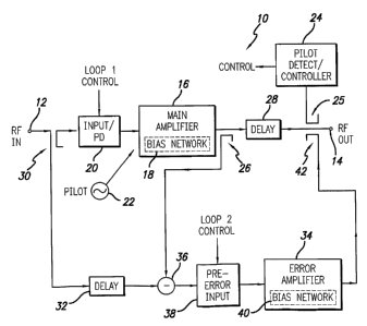
FIG. 2 is a block diagram of a preferred embodiment of a feed forward power
amplifier in accordance with the invention.
FIG. 3 is a plot of the transfer characteristic of the main amplifier in the
feed
forward power amplifier of FIG. 2 illustrating the gain characteristic over
the
operating range.
FIG. 4 is another plot of the transfer characteristic of the main amplifier in
the feed
forward power amplifier of FIG. 2 illustrating the phase response over the
operating range.
FIG. 5 is a plot of the transfer characteristic of the error amplifier in the
feed
forward power amplifier of FIG. 2 illustrating the gain characteristic over
the
operating range.
FIG. 6 is another plot of the transfer characteristic of the error amplifier
in the feed
forward power amplifier of FIG. 2 illustrating the phase response over the
operating range.
FIG. 7 is a detailed schematic drawing of one preferred implementation of a
feed
forward power amplifier in accordance with the invention.
DETAILED DESCRIPTION OF THE INVENTION
A preferred embodiment of the invention is illustrated in Figures 2-6.
Referring
first to Figure 2 the forward amplifier 10 is illustrated in a block schematic
drawing.
The feed forward amplifier 10 includes an input 12 which receives an input RF
signal to be amplified and an output 14 which outputs the amplified RF signal.
The
7
CA 02476246 2004-08-11
WO 03/069773 PCT/US03/03948
RF signal may be a high bandwidth signal such as a CDMA (Code Division
Multiple Access) spread spectrum communication signal or WCDMA (Wide Code
Division Multiple Access) or other high bandwidth signal. In spread spectrum
cellular systems such as CDMA or WCDMA a number of individual channels or
users are combined and spread over a frequency spectrum by multiplying user
data with a spreading code and then combining the channels. The spreading code
is typically chosen to spread the data from an individual channel across a
relatively
wide frequency spectrum, within of course the spectrum range available to the
given cellular provider. Since many individual channels are combined, the peak
power of the overall signal provided to the amplifier 10 will depend on the
individual amplitudes of the symbols being combined. It is statistically
possible that
the individual channel symbols will add to create very large combined symbol
peaks. Although statistically not common, such very large symbol peaks must be
accommodated in the overall system design. In the amplifier 10 these signal
peaks
are accommodated in an efficient manner by exploiting their relatively
infrequent
statistical nature, as will be discussed in detail below.
Still referring to figure 2, the input RF signal is split into a main
amplifier signal
path and an error amplifier signal path at input coupler 30 in accordance with
well
known feed forward amplifier design. The main amplifier signal path includes
main
amplifier 16 which is biased in a high efficiency mode of operation via bias
network
18, as illustrated. More specifically, main amplifier 16 is biased at an
operating
power level and bias class so that good DC to RF conversion efficiency is
provided
and wasted power and heat are minimized. As a result, however, at least some
of
the signal peaks of the RF input signal will enter the nonlinear operating
region of
the amplifier transfer characteristic and the main amplifier will operate in a
clipping
mode introducing distortion for these signal peaks. These operating
characteristics
of the main amplifier 16 and the manner in which this distortion is handled by
the
error signal path will be discussed in more detail below.
The main amplifier signal path further includes input and pre-distortion
circuitry 20.
The input circuitry may include a preamplifier, group delay circuitry, and
gain and
phase control circuitry generally in accordance with conventional feed forward
8
CA 02476246 2004-08-11
WO 03/069773 PCT/US03/03948
design. The pre-distortion circuitry in turn pre-distorts the input signal to
reduce
IMDs introduced by main amplifier 16. Although the pre-distortion circuitry 20
may
be conventional in general design and operation, in combination with the main
biasing it allows the main amplifier 16 to be operated even further into its
nonlinear
regime while controlling the amount of distortion. A pilot signal source 22
provides
a pilot signal which is injected into the main amplifier input as illustrated
and is
used to control the input and pre-distortion circuitry 20. In particular, the
pilot signal
is extracted at the amplifier output by pilot sampling coupler 25 and used by
controller 24 to control the input and pre-distortion circuitry 20 to minimize
the pilot
signal in the output signal and thereby minimize distortion in the output
signal. The
main amplifier signal path further includes a main amplifier output sample
coupler
26 and delay 28, generally in accordance with conventional feed forward
design.
Additional details of the main amplifier signal path will be described below
in
relation to a detailed implementation illustrated in figure 7.
Still referring to figure 2, the error amplifier signal path includes input
signal
coupler 30 which samples the RF input signal and provides it to the error
amplifier
34 via delay 32, attenuator/combiner 36 and pre-error input circuitry 38. More
specifically, delay 32 and attenuator/combiner 36 operate as in a conventional
feed forward amplifier such that the sampled output of the main amplifier 16
is
attenuated and combined with the delayed input signal at attenuator/combiner
36
to substantially cancel all but the distortion component of the sampled signal
from
the main signal path. In some applications and implementations it may be
advantageous to control the cancellation at attenuator/combiner 36 to retain
some
RF carrier component in the resulting signal and the resulting signal is not
purely
the distortion component of the main amplifier. Nonetheless, for the purposes
of
the present application the resulting signal will be referred to as the
distortion
component and it should be understood some carrier component may be included.
This distortion component of the signal is provided to pre-error input
circuitry 38.
Pre-error input circuitry may include a preamplifier, group delay circuitry,
and gain
and phase control circuitry which operates similarly to circuitry 20. However,
unlike circuitry 20 a pre-distortion circuit is not required in the error path
due to the
highly linear nature of the error amplifier.
9
CA 02476246 2004-08-11
WO 03/069773 PCT/US03/03948
The output of circuitry 38 is provided to error amplifier 34 which restores
the
magnitude of the sampled distortion components (IMDs) to that in the main
signal
path. Error amplifier 34 includes bias network 40 which controls the operating
power range and bias class of error amplifier 34 so that it operates in a
highly
linear portion of its transfer characteristic. Since signal peaks in the input
RF signal
will create relatively large peak IMDs sampled from the main amplifier output,
the
error amplifier must be significantly larger than conventional feed forward
error
amplifiers. For example, the error amplifier may range from about one half the
size of main amplifier 16 to twice the size of main amplifier 16. This is in
contrast
to conventional error amplifiers which are typically about one ninth the size
of the
main amplifier. Also, the error amplifier must be biased in a bias class which
is of
high linearity to ensure the operation is linear in the operating portion of
the
transfer characteristic. Since the bias class of the error amplifier is high,
the error
amplifier is inherently relatively inefficient in DC to RF conversion and the
error
amplifier is potentially a significant source of wasted power and undesired
heat.
Nonetheless, in practice it has been determined that the occurrence of signal
peak
related IMDs is sufficiently infrequent that the error amplifier only acts as
a pulse
amplifier and its impact on the efficiency of the overall amplifier is
minimal.
Still referring to figure 2, the amplified distortion component output from
error
amplifier 34 is combined with the delayed main signal at 180 degrees (out of
phase) with the main amplifier output at error injection coupler 42 to cancel
the
distortion component in the main signal path. A substantially distortion free
amplified signal is then provided to the output 14. Any residual distortion is
detected by the pilot detect circuitry 24 and used by the controller to
provide
control signals to circuitry 20 and 38 under the control of controller 24
which may
be a suitably programmed microcontroller. These two controls may be
essentially
independent and may be viewed as control of two separate loops; loop1
comprising circuitry 20, main amplifier 16, main amplifier output sample
coupler
26, input signal coupler 30, group delay 32 and combiner 36, and loop 2
comprising sample coupler 26, attenuator/combiner 36, pre-error circuit 38,
error
amplifier 34, delay 28 and error injection coupler 42. More details on the
loop
CA 02476246 2004-08-11
WO 03/069773 PCT/US03/03948
control operation will be provided in relation to a preferred detailed
implementation
described in relation to figure 7.
Referring next to figures 3-6 and below Table 1, the operating characteristics
of
main amplifier 16 and error amplifier 34 will be described in more detail.
These
figures and Table 1 assume that 100 Watt P1dB devices, specifically 100 Watt
LDMOS (Laterally Diffused Metal Oxide Semiconductor) amplifier devices with
saturation at about 1dB, are used in the main and error amplifiers. Table 1
provides bias classes for the main amplifier and error amplifier in terms of
quiescent bias currents (Idd) as a percentage of saturation current (ldss) for
the
amplifier devices. Figures 3-6 in turn illustrate the transfer characteristics
for the
main and error amplifiers over their operating range. Although these specific
values correspond to one device example, i.e. 100 watt LDMOS P1dB devices,
these bias class characteristics, operating ranges and transfer curves will
scale
quite generally across both larger and smaller devices. Accordingly, these
bias
class definitions, operating ranges and transfer curves are not limited to the
specific power example. Nonetheless, the bias class definitions of Table 1 may
not
specifically correspond to the Table 1 device parameters for all amplifier
device
types. The distinction between bias classes and the definition of class C,
class
AB2, class AB1 and class A are generally understood in the art for a wide
variety
of devices, however, and therefore the Table 1 device parameter values should
be
viewed as illustrative and not limiting in nature.
Table 1:Nominal Quiescent Bias Currents, per device, at 25 C
Idss 12.0 Amp
Main Min Main Max Error Min Error Max
Class of Idd % Idd % Idd % Idd % Idss
Operation (Amp) Idss (Amp) Idss (Amp) Idss (Amp)
C 0.000 0.00% 0.020 0.17%
AB2 0.150 1.25% 0.300 2.50%
A131 0.400 3.33% 1.200 10.00
A 1.200 10.00 3.000 25.00
11
CA 02476246 2004-08-11
WO 03/069773 PCT/US03/03948
As may be seen from Table 1, the main amplifier is biased in a high efficiency
class, specifically Class C or lower Class AB (AB2). This provides the desired
maximum DC to RF conversion efficiency for a given device size. In addition to
reducing wasted power, this DC to RF efficiency increases reliability. More
specifically, when modern RF power devices such as LDMOS amplifier devices
are operated at higher efficiency levels this directly translates into lower
junction
temperature. Reduction in junction temperature greatly increases the mean
lifetime of the device and thus improves overall reliability of the feed
forward power
amplifier system. The transfer curves of figures 3 and 4 in turn show that
some
nonlinearity in the transfer characteristic occurs throughout the normal or
average
power operating range of the main amplifier due to the biasing class of the
main
amplifier (especially in the power vs gain transfer curve). This nonlinearity
will
introduce some distortion (IMDs) through the normal operating range. However,
as
shown in figure 3, this nonlinearity is only about .5 dB gain or less through
this
average power region of the transfer curve; i.e., between P1dB-20 and P1dB-10
in
the specific example illustrated. Therefore, this average power region may be
characterized as a substantially linear region of the transfer curve. By the
use of
pre-distortion in the main path IMDs due to this nonlinearity can be
substantially
eliminated. Therefore, there will be minimal load on the error amplifier
during
operation in the average power region.
The transfer curves of figures 3 and 4 also show that the average power region
of
the main amplifier transfer curve is chosen relatively close to the saturation
point
of the amplifier. Therefore, for a given power requirement a smaller device
can be
used. Since smaller devices have lower current and draw less power the DC to
RF
efficiency is further increased. As may be seen from the transfer curves,
however,
while average signal power levels correspond to operation in the substantially
linear portion of the transfer characteristic, the randomly occurring peak
power
signals are in a highly nonlinear portion of the transfer characteristic. This
portion
of the operating region corresponds to significant IMDs in the main amplifier
output
which are too large to be removed by pre-distortion in the main path. As
discussed
above, however, these signal peaks are relatively infrequent for typical high
bandwidth signals, such as CDMA and WCDMA RF input signals. Therefore, the
12
CA 02476246 2004-08-11
WO 03/069773 PCT/US03/03948
main amplifier 16 operates in a high efficiency substantially linear mode the
majority of the time but generates intermittent large IMD products. These
intermittent large IMD products in turn must be removed from the RF output by
the
operation of the error amplifier.
Referring to Table 1 and figures 5 - 6, the error amplifier operating
characteristics
will next be described. Table 1 shows that the bias class for the error
amplifier is
significantly higher than for the main amplifier, e.g., higher AB (AB1) or
Class A.
Also, the size of the error amplifier is selected so that the majority of the
operating
range is well away from the nonlinear portion of the transfer curve near peak
power. In some demanding applications the error amplifier may be larger than
the
main amplifier, up to about double the main amplifier size. Alternatively, in
less
demanding applications the error amplifier may be smaller than the main
amplifier,
e.g., about half the main amplifier. This combination of error amplifier size
and bias
class provides a linear transfer characteristic for the error amplifier over
substantially all of its operating range, including signal peaks, as shown in
figures
5 and 6. This allows the error amplifier to accurately amplify peak signal
IMDs so
as to cancel the main amplifier distortion. Therefore, amplifier 10 provides
an RF
output substantially free of IMDs throughout the operating range of the RF
input,
including signal peaks. Although the bias class and operating range of the
error
amplifier are selected for maximum linearity and not efficiency, nonetheless
the
overall efficiency of the feed forward amplifier will not be significantly
affected
since the signal peaks are intermittent in nature. That is, the error
amplifier
effectively acts in a pulse mode with relatively low total power consumption.
Although the error amplifier transfer curve of figure 5 shows a linear
response
through less than all the operating range, about 25 -26 dB of the 30 dB
operating
range (i.e., to about - 4 to -5 dB from peak device power taken to be 1 dB) in
practice this will catch virtually all of the signal peak IMDs since peaks
outside this
power range will be extremely rare. Nonetheless, this linear range may be
varied
somewhat depending on the statistics of the peak power pulses for the specific
type of RF input signal and the IMD tolerance of the particular application.
The
phase response of figure 6 is less critical but again the linear region may
varied
13
CA 02476246 2004-08-11
WO 03/069773 PCT/US03/03948
with the application. In particular, the linear portion of the operating range
of the
error amplifier transfer curve may be increased by increasing the size of the
error
amplifier thereby moving the entire operating range further to the left in
figures 5
and 6. Therefore, it will be appreciated that if needed for a particular
application
the linear portion of the error amplifier transfer curve may extend through
the
entire operating range including the entire peak signal range.
Accordingly, it will be appreciated that the present invention provides a feed
forward amplifier with high efficiency and minimal wasted power and unwanted
heat generation while at the same time providing the high degree of linearity
needed for wide bandwidth applications.
Referring to figure 7, a specific implementation of the feed forward power
amplifier
of figure 2 is illustrated. This specific embodiment corresponds to equal size
main
and error amplifier modules 16, 34, respectively, although the operating
characteristics of the two modules will be very different as discussed in
detail
above. This may have cost advantages due to the use of the same basic
amplifier
module configuration, thereby avoiding separate design and tooling costs and
costs associated with separate manufacturing steps for the two modules.
Performance requirements may offset the cost advantages in certain
applications,
however, and the ratio of main to error amplifier size may be from one-to-two
to
two-to-one, as discussed above. Also, the specific implementation of figure 7
shows a specific dual control loop configuration including main and error path
predistortion, which may reduce distortion due to signal peaks and improve
overall
amplifier efficiency.
More specifically, as illustrated in figure 7 the main amplifier path includes
RF
input 12, input signal coupler 30, input and pre-distortion circuitry 20,
pilot injection
coupler 107, main amplifier power module 16, main amplifier output sample
coupler 26, group delay line 28, error injection coupler 42, pilot detect
coupler 25,
isolator 114, and RF output 14. The input and pre-distortion circuitry 20 in
the
illustrated embodiment comprises distributed small signal gain stages 102,
group
delay adjusting circuit 103, pre-distortion circuits 104, phase control
circuit 105,
14
CA 02476246 2004-08-11
WO 03/069773 PCT/US03/03948
and amplitude control circuit 106. Distributed small signal gain stages 102
may be
conventional and operate to provide a small initial gain to the RF input
signal.
Group delay adjusting circuit 103, pre-distortion circuit 104, phase control
circuit
105, and amplitude control circuit 106 operate under the control of controller
230
which may be a suitably programmed microcontroller. Controller 230 receives
the
detected pilot signal from pilot detect circuit 115 and employs this signal to
adjust
the group delay adjusting circuit 103, pre-distortion circuit 104, phase
control
circuit 105 and amplitude control circuit 106 to minimize the pilot signal and
hence
minimize distortion. Controller 230 also may provide a signal to pilot
generator 22
which is used to create the pilot signal. In accordance with typical feed
forward
control this action may be best described as one loop of a two loop control
process
as discussed below. The main amplifier power module 16 includes main amplifier
stages 110, 111, 112, and 113 biased, as discussed in relation to Table 1
above,
in class C or AB2. This four stage implementation corresponds to four separate
devices; e.g. a pre-amplifier 110, an intermediate power amplifier 111, and
two
large power amplifiers 112, 113, e.g. 100 Watt 1dB main amplifier LDMOS
stages.
It will be appreciated that more or fewer stages may be employed depending on
the application and power requirements and on the available stage amplifiers
performance and cost.
Still referring to figure 7, the error amplifier path includes group delay
line 32,
carrier cancellation offset injection coupler 202, carrier cancellation
detector 203,
carrier cancellation coupler 206, error input signal sample coupler 207, error
input
signal test port 209, pre-error input 38, error amplifier power module 34, and
output error amplifier interconnection lines 216 to the error injection
coupler 42.
The carrier cancellation coupler 206 receives the sampled and attenuated main
amplifier output from main amplifier output sample coupler 26, main sampled
signal attenuator 210 and associated RF interconnections 217. The carrier
cancellation detector 203 detects the amount of RF carrier in the error path
and
provides this as an input to controller 230. A test signal may be applied to
the error
path via test port 209. The pre-error input circuitry 38 comprises distributed
small
signal gain stages 208, group delay adjuster circuit 211, phase adjustment
circuit
214 and amplitude adjustment circuit 213. The distributed small signal gain
stages
CA 02476246 2004-08-11
WO 03/069773 PCT/US03/03948
208 may be conventional in operation. The group delay adjuster circuit 211,
phase
adjustment circuit 214 and amplitude adjustment circuit 213 operate under the
control of controller 230, as discussed below. The error signal is provided
from
pre-error input circuitry 38 to error amplifier power module 34. Error
amplifier
power module 34 comprises stages 220, 221, 222, and 223 corresponding to the
main module 16 layout in the illustrated equal size main and error
implementation.
These stages 220, 221, 222, and 223 may comprise devices, e.g. LDMOS
amplifier devices, of the same size as in the main module but differently
biased. In
particular, as discussed above in relation to Table 1, the stages 220, 221,
222, and
223 may comprise LDMOS amplifiers biased in class AB1 or A. This will provide
highly linear amplification of the error signal for current high bandwidth
applications. If future even higher bandwidth requirements or higher power
applications increase the error signal input the error amplifier size may be
increased to maintain the linearity across the operating range, as discussed
above
in relation to figures 5 and 6. The amplified error signal is then applied via
error
amplifier output interconnection lines 216 to the error injection coupler 42
where it
cancels IMDs in the main path.
The following discussion of the specific control implementation of figure 7
will
clarify the use of the controller 24 and circuitry 20 and 38 to help achieve
desired
IMD performance. As discussed above, this control may be viewed as separate
control of two loops in accordance with conventional feed forward control
terminology. The first control loop (or loop 1) is the carrier cancellation
loop in
accordance with conventional terminology. Loop 1 contains the following
circuit
elements:
Input signal coupler 30
Distributed small signal gain stages 102
Main path group delay adjusting circuit 103
Main path pre-distortion circuit 104
Main path phase 105 and amplitude 106 control circuits
Pilot injection coupler 107
Main amplifier power module 16
16
CA 02476246 2004-08-11
WO 03/069773 PCT/US03/03948
Main amplifier output sample coupler 26
Associated main output RF interconnections 217
Sampled signal attenuator 210
Group delay line 32
Carrier cancellation offset injection coupler 202
Carrier cancellation detector 203
Carrier cancellation coupler 206
Error input signal sample coupler 207
Error input signal test port 209.
Loop 1 carrier cancellation detector 203 behavior is similar to a conventional
feed
forward power amplifier system. The controller 230 adjusts the group delay
circuit
103 and phase and amplitude control circuits 105, 106 to set the detected
carrier
signal at carrier cancellation circuit 203 to a desired level. Controller 230
may
operate so that when the carrier cancellation is adjusted there is a minimum
amount of RF energy incident upon the,input of the carrier cancellation
circuit 203.
As noted above, however, in some applications it may be advantageous to adjust
the carrier cancellation so that some RF carrier component remains. Loop 1 pre-
distortion circuit 104 is controlled by controller 230 by monitoring the pilot
signal
from pilot detect circuit 115 to minimize the detected pilot signal.
Loop 2 is the error path loop or auxiliary path loop. Loop 2 contains the
following
circuit elements:
Main amplifier output sample coupler 26
Loop 2 group delay line 28
Main sampled signal attenuator 210 and associated RF interconnections
217
Carrier cancellation coupler 206
Error path input signal sample coupler 207
Distributed small signal gain stages 208
Group delay adjuster circuit 211
Phase 214 and amplitude 213 adjustment circuits
17
CA 02476246 2004-08-11
WO 03/069773 PCT/US03/03948
Error amplifier power module 34
Output Error Amplifier interconnection lines 216
Error injection coupler 42.
Loop 2 actions are controlled by operation of controller 230. As the case of
Loop 1
the detected pilot signal is used to monitor and adjust loop 2 cancellation
performance. Those skilled in the art will appreciate details of pilot
requirements in
order to control loop 2 performance and stability of circuits 211, 213 and
214. Pre-
distortion circuit 104 is used under control of controller 230 by minimizing
the
detected pilot signal together to improve AM/AM and AM/PM performance due to
higher output power levels. The use of a main path pre-distortion circuit thus
improves IMD to carrier ratio at higher output power levels.
A preferred embodiment of the present invention of an RF power amplifier
design
which provides both high efficiency and minimal distortion in broad bandwidth
RF
applications has been described in relation to the various figures.
Nonetheless, it
will be appreciated by those skilled in the art that a variety of
modifications and
additional embodiments are possible within the teachings of the present
invention.
For example, a variety of specific feed forward circuit implementations and
loop
controller implementations may be provided employing the teachings of the
present invention and limitations of space prevent an exhaustive list of all
the
possible circuit implementations or an enumeration of all possible control
implementations. A variety of other possible modifications and additional
embodiments are also clearly possible and fall within the scope of the present
25, invention. Accordingly, the described specific embodiments and
implementations
should not be viewed as in any sense limiting in nature and are merely
illustrative
of the present invention.
18