Note: Descriptions are shown in the official language in which they were submitted.
CA 02476363 2004-07-30
r
DOCKET NO.: 4727
INVENTORS: Matthias BOPP
Stephan GERLACH
TITLE OF THE INVENTION
Transmitting and Receiving Arrangement With at Least Two Pairs
of Respectively One Transmitting Power Amplifier and One Low
Noise Input Amplifier
s PRIORITY CLAIM
This application is based on and claims the priority under 35
U.S.C. ~119 of German Patent Application 103 36 292.4, filed on
August 1, 2003, the entire disclosure of which is incorporated
herein by reference.
~o FIELD OF THE INVENTION
The invention relates to a transmitting and receiving arrangement
having at least two pairs of respectively one transmitting power
amplifier and one low noise input amplifier, whereby the
respective pairs of amplifiers are respectively allocated to
1s different frequency ranges, and whereby respectively at least one
transmitting power amplifier and at least one low noise input
amplifier are combined or incorporated in a common structural
unit. The invention further relates to a method for operating
such a transmitting and receiving arrangement.
9727/WFF:ar - 1 -
5
CA 02476363 2004-07-30
BACKGROUND INFORMATION
It is generally known in the art to combine a transmitting power
amplifier with a low noise input amplifier on a common
semiconductor substrate. The power amplifier and the low noise
s amplifier thus together form a common structural unit, which is
generally embodied as a monolithic integrated circuit based on
any one of different conventional technologies, for example, most
often based on silicon technology or gallium-arsenide variations.
The monolithic integration of a low noise input amplifier (also
~o simply called an input amplifier or a low noise amplifier (LNA)
herein)-and a transmitting power amplifier (also simply called
a transmitting amplifier or a power amplifier (PA) herein) on a
common semiconductor substrate material achieves various
advantages, such as a reduction of the surface area occupied by
~s the components, simplification and economization of the
fabrication, among other known advantages.
On the other hand, such monolithic integration of the power
amplifier with the low noise amplifier in the same structural
unit also causes a significant disadvantage. Particularly,
zo during the transmitting operation, the active transmitting power
amplifier generates and dissipates a substantial amount of heat
due to its electrical power loss or dissipation, which
consequently heats the entire structural unit based on the common
semiconductor substrate, including the low noise input amplifier.
Zs Since the transmitting power amplifier typically operates with
4727/WFF:ar - 2
CA 02476363 2004-07-30
a power much higher or even a substantial multiple of the power
of the low noise input amplifier, the input amplifier is actually
heated to a significantly higher temperature in the transmitting
operation (due to the heat dissipation by the power amplifier)
s than during pure receiving operation (due to the power
dissipation of the low noise input amplifier). In this regard,
typical power values are about 300 mW for transmitting operation
and about 10 mW for receiving operation.
The above mentioned heating of the low noise input amplifier
~o directly leads to a physically necessitated increase of the noise
factor, a drift of the characteristic values or parameters, and
an overall deterioration of the reception characteristics of the
system. Even with a time-offset or time-shifted operation (time
slot method) of the two amplifier components integrated on one
~s chip, i:e. alternating transmission and reception, a substantial
heating of the low noise amplifier still arises, due to the
thermal store or reservoir behavior of the semiconductor
material. This undesirably also applies the heating effect of
the transmitting amplifier's power dissipation to the low noise
zo input channel amplifier.
The thermally induced increase of the noise factor F occurs
according to the general formula F = K x T x B, wherein F is the
noise factor, K is Boltzmann's constant, T is the temperature,
and B is the frequency bandwidth of the low noise input amplifier
2s being considered. In order to reduce or avoid the above
mentioned undesirable influences of the heating of the low noise
4727/wFF:ar - 3
CA 02476363 2004-07-30
amplifier, in special applications such as space travel and radio
astronomy, special cooling arrangements are used to cool the low
noise input amplifier down to nearly absolute zero temperature.
Such special cooling arrangements, however, are quite complicated
s and costly. Such effort and expense cannot be utilized, already
for reasons of cost, in the general field of consumer goods, or
especially in connection with mobile telephones, for example GSM
(Global System for Mobile Communications) telephones, and
wireless data transmission systems such as WLAN (Wireless Local
~o Area Network) applications.
To avoid the above mentioned cross-heating of the low noise input
amplifier by the dissipated heat of the power amplifier mounted
on the same chip, it is also conventionally known to arrange the
low noise input amplifier on a first receiver chip, and to
~s arrange the- transmitting power amplifier on .a separate second
transmitting chip. Due to the spatial separation of the two
chips, the receiver chip is not so strongly heated by the
operation of the transmitter chip, in comparison to the
arrangement with both amplifiers integrated on a single chip.
2o While this achieves the advantage of a reduced heating of the
input or receiver chip during operation of the transmitter chip,
it necessarily brings about significant disadvantages by
requiring two separate chips. Namely, such an arrangement fails
to achieve the advantages of a monolithic integration of several
2s amplifiers on a single chip as discussed above.
A727/WFF:ar - 4 -
CA 02476363 2004-07-30
SUN.~'IARY OF THE INVENTION
In view of the above, it is an object of the invention to provide
a transmitting and receiving arrangement, and a device including
such a transmitting and receiving arrangement, with a reduced
s heating of a low noise input amplifier due to the operation of
a transmitting power amplifier. The inventive arrangement shall
maintain or achieve the advantages (e. g. the space or volume
reduction and the cost reductian) of a monolithic integration of
at least one low noise input amplifier and at least one
~o transmitting power amplifier on a single chip or in a single
integrated circuit on a common substrate,. Another object of the
invention is to provide a method of operating such a transmitting
and receiving arrangement t'o reduce the cross-heating of the low
noise input amplifier due to the heat dissipation of the
~s transmitting power amplifier. The invention further aims to
avoid or overcome the disadvantages of the prior art, and to
achieve additional advantages, as apparent from the present
specification. The attainment of these objects is, however, not
a required limitation of the claimed invention.
2o The above objects have been achieved according to the invention
in a device including a transmitting and receiving arrangement
with at least two pairs of respectively one transmitting power
amplifier and one low noise input amplifier, wherein the pairs
of amplifiers are respectively allacated to different frequency
zs ranges, and wherein respectively at least one transmitting power
amplifier and at least one low noise input amplifier are combined
47271WFF:ar - 5
CA 02476363 2004-07-30
or incorporated in a single common structural unit. Especially
according to the invention, the low noise input amplifier and the
transmitting power amplifier of a given pair allocated to and
adapted to operate in a specified frequency range are
s respectively incorporated in different structural units. For
example, the transmitting power amplifier operating in a first
frequency range is incorporated in a first structural unit, while
the low noise input amplifier operating in this first frequency
range is incorporated in a second structural unit separate from
~o the first structural unit. Moreover, the low noise input
amplifier incorporated in the first structural unit operates in
a frequency range different from the first frequency range.
The above objects have further been achieved according to. the
invention in a method of operating the transmitting and receiving
15 arrangement in one. of the above mentioned frequency ranges,
wherein the amplification of received signals in this frequency
range is carried out using the low noise input amplifier
incorporated in one of the structural units or chips, while the
amplification of output signals to be transmitted is carried out
2o using the transmitting power amplifier incorporated in a
different one of the structural units or chips. Thereby the
input amplifier and the transmitting amplifier being used for
this communication are both allocated to the same frequency range
and thus form a frequency-based pair of amplifiers, yet are
2s physically located and incorporated in two different and separate
chips.
4727/WFF:ar - fi -
CA 02476363 2004-07-30
The above features of the invention achieve a physical or spatial
separation of the transmitting functions and the receiving
functions within a given frequency range, while still also
providing a structural incorporation or integration of a
s transmitting power amplifier and a low noise input amplifier on
each individual chip. Due to the physical or spatial separation
of the two amplifiers allocated to a particular frequency range
or a particular frequency, the input amplifier used for this
frequency range will not be heated by the operation of the
~o transmitting amplifier that is active in this frequency range.
Namely, the physical or spatial separation, and optionally the
arrangement of a thermally insulating material therebetween,
consequently provides a thermal isolation between the two
ampli:f iers. Thus, the signal-to-noise ratio of the active input
15 amplifier is not significantly deteriorated (due to heating):-by
the active transmitting power amplifier. The invention further
achieves all the advantages of integrated fabrication of input
(or receiving) and output (or transmitting) amplifiers together
on a single chip, in an arrangement of several such chips in
2o devices that are adapted to operate selectively in any selected
one of plural frequency ranges, such as multi-frequency,
multi-band, or multi-mode mobile telephones or data
transmitting/receiving devices.
It is especially preferred according to the invention that each
2s structural unit is embodied as a common chip in which at least
one of the transmitting power amplifiers and at least one of the
low noise input amplifiers are incorporated or integrated. An
9727/WFF:ar - 7 -
CA 02476363 2004-07-30
advantage of this embodiment is that transmitting power
amplifiers and low noise input amplifiers can be economically and
efficiently realized together in a monolithic integrated circuit
from a viewpoint of the fabrication processes and techniques,
s without causing the above discussed conventional disadvantages
arising from an increase of the operating temperature of the
input amplifier and thus an increase of the noise factor or a
drift of the characteristic operating parameters of the input
amplifier.
~o In principle, the advantage of the monolithic integration becomes
ever greater the more that the utilized semiconductor fabrication
technologies have characteristics that are suitable for both the
transmitting power amplifiers with high operating power and
efficiency as well as input amplifiers with low ni~ise =factors.
15 The apparent conflict of goals or purposes between a high
operating power and efficiency of the power amplifier and a low
noise factor of the input amplifier is being ever further reduced
in modern transmission or communication systems such as GSM-EDGE
(Enhanced Data for GSM Evolution), UMTS or generally CDMA (Code
2o Divisional Multiple Access), because these systems use modulation
techniques or processes on the transmission side, which also
contain data or transmission informations in the envelope curve
of the signal. As~a result, however, the demands on the
linearity of the transmitting power amplifier are significantly
2s increased.
4727/WFF:ar - 8 -
CA 02476363 2004-07-30
For that reason, transistors of the transmitting power amplifier
are generally no longer operated in the efficiency-optimized
C-operating mode (class C), but rather more often in the
A-operating mode (class A~, which exhibits an improved linearity
s between the amplifier input signal and the amplifier output
signal. The improvement of the linearity, however, comes at the
expense of the operating efficiency, which, for physical reasons,
is lower in the A-operating mode than in the compressed or
optimized B- or C-operating modes of a transistor amplifier.
~o A further characteristic that is demanded for this type of
transmitting power amplifiers, is the lowest possible noise or
interference spectrum in the range of adjacent channels, which
ultimately can be interpreted as a demand for a low noise vfactor.
Thus,:, the requirements-or demands for a combination technol:bgy
~s for integrating transmitting power amplifiers and low noise input
amplifiers on a common monolithic chip are identical to each
other at least with respect to certain essential aspects. For
that reason, both types of amplifiers can be combined in a common
integrated circuit in a space-saving manner in an economical and
2o efficient fabrication process.
However, due to the reduced operating efficiency of the
transmitting power amplifier with the same output power, the
result is an increased thermal dissipation and thus an increased
temperature of the chip in which the transmitting power amplifier
is is incorporated. In principle, this would teach away from such
an integration of the amplifiers. Nonetheless, according to the
4727/WFF:ar - 9
CA 02476363 2004-07-30
invention, any such increased heat dissipation that might arise
is not problematic. Namely, it is exactly the combination
achieved by the integration of at least one low noise input
amplifier and at least one transmitting power amplifier on a
s common chip, in connection with the distribution or separation
of the transmitting functions and the receiving functions for a
given frequency range onto two separate chips, which in sum
achieves a reduced noise factor of the law noise input amplifier
active at a particular frequency, despite the monolithic
~o integration thereof with a transmitting power amplifier (for a
different frequency range) on the same chip.
Moreover; this distribution or separation of the transmitting and
receiving functions onto separate chips achieves the advantage
of multiple utilization and combination of functional units that
would otherwise be redundant in the circuit blocks (e.g. the
transceivers) that generate and/or process the signals being
transmitted and/or received. This is a significant goal to be
strived for, especially for achieving a reduction of costs as
well as space saving. An example in which such an application
2o is significant is in wireless local area networks (WLAN)
operating at 2.4 and 5.2 GHz.
It is further preferred in a particular embodiment of the
invention, that the transmitting power amplifier and the low
noise input amplifier are realized as monolithic integrated
2s circuits on a silicon basis or a gallium-arsenide basis . Through
these features, the inventive arrangement can be economically
4727JWFF:ar - 10 -
CA 02476363 2004-07-30
fabricated using well-developed fabrication techniques in high
volumes or piece counts. As a result, the inventive arrangement
can be widely and economically utilized and incorporated into
various different devices in various fields.
s A further preferred embodiment feature of the invention involves
the integration of the amplifiers in structural units embodied
as bonded integrated circuits, as a flip-chip in a housing, or
in the form of modules on a separate substrate carrier. As is
generally known, a bonded chip or bonded integrated circuit is
~o an integrated circuit that is contacted via band wires. A
flip-chip, as conventionally known, refers to a semiconductor
wafer with planar diodes or transistors, of which the contacts
or connection points are disposed on the backside of the chip.
Such flip-chips can be -installed in thin film -or thick film
~s circuits, and represented a transition stage leading to
integrated circuits . In any event, any of these technologies and
structural arrangements can be used to provide each structural
unit according to the invention. All three of these concrete
realizations are well suited to carrying out an economical high
zo volume series production.
It is also preferred that the device in which the transmitting
and receiving arrangement according to the invention is
incorporated, is a mobile telephone or a portable data
communication device. In either case, the device is suitable and
zs adapted to be used or operated in plural frequency ranges. It
is especially preferred that the various different frequency
4727 J'nTFF: ar - 11 -
CA 02476363 2004-07-30
ranges are the dual-band or tri-band frequency ranges for mobile
telephones, or industrial, scientific or. medical ISM frequencies
that are usable without a license, or other multi-mode or
multi-band applications and/or combinations of mobile telephones
s with cordless telephones. These applications all offer only a
small installation space or volume, while also requiring that
transmitting and receiving arrangements adapted for use in plural
different frequency bands with good reception and transmission
quality must be arranged within the available limited
~o installation volume. Through the invention, these
characteristics can be achieved at a cost that is acceptable in
the market for such devices.
Another preferred feature of the invention is that the
transmitting.po~aer amplifier in a particular-structural unit is
~s not operated together with the low noise input amplifier provided
in this same structural unit, during a given communication or
transmission connection. This means that the transmitting
amplifier and the input amplifier included in a given structural
unit will not both be operated at the same time, and even not
2o during the same communication or transmission connection, e.g.
in a time-alternating manner such as in a time slot process.
This reliably prevents an undesirable heating of an input
amplifier active for a particular frequency by the dissipated
heat of a transmitting power amplifier arranged on the same chip
2s as this input amplifier. Since the transmitting power amplifier
arranged on the same chip is allocated to a different frequency
or different frequency range in comparison to the input amplifier
4727/WFF:ar - 12 -
CA 02476363 2004-07-30
on this chip, and the different frequency ranges are used
individually, separately and selectively, one at a time, the
cross-heating problem is avoided. Also, the functionality of the
application will thereby not be substantially diminished or
s deteriorated.
It should be understood that the several features of the
invention described herein are not limited to the respectively
described combinations, but rather can also be provided in
different combinations or even individually, still within the
~o scope of the present invention.
BRIEF DESCRIPTION OF THE DRAWING
Tn order that the invention may be clearly understood, it will
now bedescribed in connection with an example embodiment
thereof, with reference to the single accompanying drawing
15 Figure, which schematically illustrates a block diagram of the
basic structure of a transmitting and receiving arrangement
according to an example embodiment of the invention.
DETAILED DESCRIPTION OF A PREFERRED EXAMPLE EMBODIMENT AND OF THE
BEST MODE OF THE INVENTION
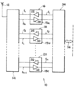
zo The single drawing Figure shawl a transmitting and receiving
arrangement 10 that receives and/or transmits signals via an
antenna 12. Thus, the transmitting and receiving arrangement 10
is especially or preferably a wireless transmitting and receiving
4727/rnTFF:ar - 13 -
CA 02476363 2004-07-30
arrangement. The antenna 12 is selectively connected via an
antenna circuit selector switch 14 to a group or ensemble of
separate individual chips 16, 18 and 20. Each one of these chips
16, 18 and 20 respectively includes at least one transmitting
s power amplifier 22, 24 or 26 and at least one low noise input
amplifier 28, 30 or 32 respectively incorporated in the
structural unit embodied by the respective chip. For example,
each one of the chips respectively includes at least one of the
power amplifiers and at least one of the input amplifiers mounted
~o on a common carrier, or formed on a common substrate, or
integrated in the same circuit or overlapping circuits. Note
that the three chips 16, 18 and 20 are merely representative of
any number n of chips that may be provided, where this number n
is at least two according to the present invention.
~s In the drawing Figure, the individual chips l6, 18 and 20 have
merely been schematically and qualitatively illustrated.
Thereby, especially the illustrated symmei~rical size distribution
or proportionality between the low noise input amplifiers 28, 30
and 32 and the transmitting power amplifiers 22, 24 and 26 does
zo not correspond to the actual proportions of these components in
a real chip structure. To the contrary, in a real or actual
physical chip structure, the transmitting power amplif~.ers 22,
24 and 26 each occupy a substantially larger surface area than
the low noise input amplifiers 28, 30 and 32.
zs On one side thereof, each chip 16, 18 and 20 is connected by two
transmission paths, e.g. two conductors, to the antenna circuit
4727/WFF:ar - 1 4 -
CA 02476363 2004-07-30
selector switch 14. One conductor respectively connects the
output of the power amplifier 22, 24 and 26 to the antenna
circuit selector switch 14, and one conductor respectively
connects the selector switch 14 to the input of the input
s amplifier 28, 30 and 32. On the opposite side, namely the side
19a, 19b and 19c oriented away from the antenna circuit selector
switch 14 with regard to the circuit connection, each chip 16,
18 and 20 is connected by two transmission paths, e.g. two
conductors, to a transmitter/receiver component or transceiver
~0 34: Namely, one conductor connects the transceiver 34
respectively to the input of each power amplifier 22, 24 and 26,
while one conductor connects the output of each respective input
amplifier 28, 30 and 32 to the transceiver 34.
Further, the transceiver 34 is connected through a suitable
15 interface 36 with any. other circuit, component, or system
external to the transmitting and receiving arrangement 10,
whereby the transceiver 34 outputs the data and/or voice signals
received via the antenna 12 and/or receives data and/or voice
signals that are to be transmitted from the antenna I2. Thus,
zo schematically, the interface 36 represents the connection to the
remainder of any device in which the inventive transmitting and
receiving arrangement 10 may be incorporated.
The transmitting and receiving arrangement 10 is adapted to
receive and/or transmit data and/or voice signals in any selected
zs one of plural available frequency ranges. Particularly, the
arrangement 10 includes the plural transmitting power amplifiers
4727/WFF:ar - 15 -
CA 02476363 2004-07-30
22, 24 and 26 that are respectively adapted (e.g. configured,
dimensioned and tuned) to amplify signals to be transmitted
respectively in three different frequency ranges. In other
words, each transmitting power amplifier 22, 24 and 26 operates
s in a different frequency range compared to the other transmitting
power amplifiers. Similarly, the plural low noise input
amplifiers 28, 30 and 32 are respectively adapted to amplify
received input signals in three different frequency ranges.
Throughout this application; the respective different frequency
~o ranges may be completely separate non-overlapping ranges, or may
be partially overlapping ranges, or may respectively invalve
different particular tuned frequencies.
The particular circuitry involved in select~.ng the transmitting
power amplifier 22, 24 or 26 and the low noise input amplifier
15 28, 30 or 32 to be used for transmitting and receiving in a
particular communication in a given or selected frequency range
is not illustrated in detail, but ca.n be embodied in any
conventionally known or future developed manner within the
selector switch 14 and/or the transceiver 34. Since such
Zo selector arrangements will be understood by persons skilled in
this field, and the details thereof are not crucial to the
present invention, such details need not be disclosed herein.
A respective pair of amplifiers, respectively including one
transmitting power amplifier 22, 24 or 26 and one low noise input
2s amplifier 28, 30 or 32, is respectfully allocated to each
frequency range that is to be made available for selection and
4727/wFF:ar - 1 6 -
CA 02476363 2004-07-30
use in the inventive arrangement 10. For n frequencies or
frequency ranges, preferably n chips 16, 18 and 20 are used in
the arrangement 10. In that regard, the allocation can be a
one-to-one mutually unique or unambiguous allocation, so that
s exactly one transmitting power amplifier 22, 24 or 26 is
respectively allocated to and paired with exactly one input
amplifier 28, 30 or 32, and vice versa, respectively for each
individual frequency range. Alternatively, there could be a
one-to-two or two-to-one allocation among the input amplifiers
~o and the power amplifiers. Thus, the term "pair" of amplifiers
as used herein should not be restricted to a closed set of
exactly two amplifiers . Instead, the amplifiers can be organized
in a "group" for each frequency range, wherein each "group" may
include; for example, one transmitting amplifier and one input
~,s amplifier, or one transmitting amplifier and two input
amplifiers, or two transmitting amplifiers and one input
amplifier, etc., as a broader meaning of the term '°pair".
The illustrated embodiment shown in the single drawing Figure
involves the one-to-one mutually unique allocation and pairing
zo of input and transmitting amplifiers. particularly, the first
chip 16 is adapted to handle (i.e. amplify) a transmitting
frequency fl and a receiving or input frequency fn, the second
chip 18 is adapted to handle a transmitting frequency f2 and an
input frequency fl, and the nth chip 20 is adapted to handle a
2s transmitting frequency fn and an input frequency fn-1. It will
thus be apparent that each chip 16, 18 or 20 handles respectively
different frequencies on the input side and the output side, and
4727/WEF:ar - 17 -
CA 02476363 2004-07-30
correspondingly that the transmitting amplifier 22, 24 or 26 and
the input amplifier 28, 30 or 32 paired with each other by being
allocated to a given frequency are located not on the same chip,
but rather on separate chips 16, 18 and 20.
s In the present example, if there are a total of three chips 16,
18 and 20, with three amplifier pairs for handling three
different frequencies ar frequency ranges, the number or suffix
n is taken as 3. Thus, the input side of the first chip 16
handles the frequency f3, the transmitting side of the third chip
~0 20 handles the frequency f3, and the input side of the third chip
20 handles the frequency f2.
In this structure, a first pair of i~ransmitting and input
amplifiers is formed.by ahe transmitting power amplifier 22 and
the input amplifier 30, which respectively amplify signals at the
15 frequency or in the frequency range fl. A second amplifier pair
is formed by the transmitting power amplifier 24 and the input
amplifier 32 allocated to the frequency range f2 (i.e. fn-1 when
n is 3). A third amplifier pair is formed by the transmitting
power amplifier 26 and the input amplifier 28 allocated to the
2o frequency range fn (or f3 in the example in which n is 3).
As mentioned above, in this example embodiment, respectively one
transmitting amplifier 22, 24 or 26 is combined and structurally
incorporated with respectively ane input amplifier 28, 30 or 32
in one respective chip 16, 18 or 20 to form a respective
2s individual structural unit. Nonetheless, the input amplifier
4727/WFF:ar - 1$ -
CA 02476363 2004-07-30
(e. g. 30) of each respective frequency-allocated amplifier pair
( a . g, the first pair for frequency range f 1 ) is located in a
different structural unit ( a . g. chip 18 ) t,han the structural unit
(e. g, chip 16) in which the associated transmitting power
s amplifier (e. g. amplifier 22) for this frequency is located.
Alternatively, each individual transmitting power amplifier can
be allocated to more than one input amplifier. The same is true
in the reverse also, i.e. vice versa, so that more than one
transmitting power amplifier can be allocated to each individual
~o input amplifier. This choice simply depends on how many
amplifiers are needed or desired on the transmitting side and/or
on the receiving side for each given communication channel or
frequency range.
In any event, the ailocation of amplifiers on the transmitting.
~s side and the receiving side far each given frequency range;
according to the invention, is carried out so that the input
amplifier or amplifiers allocated to a particular frequency range
is or are not arranged on the same chip or chips as the
transmitting power amplifier or amplifiers allocated to this
zo frequency range. For example, a two-to-one allocation could
involve the input amplifier 28 as well as the transmitting
amplifiers 24 and 26 being allocated to a particular frequency
range.
It is to be understood that the invention is not limited to a
is transmitting and receiving arrangement structure having exactly
three chips 16, 18 and 20 in connection with one antenna 12 and
4727/WFF:ar - 19 -
CA 02476363 2004-07-30
one transceiver 34. Most basically, it is simply essential that
at least one transmitting power amplifier 22, 24, 26 and at least
one input amplifier 28, 30, 32 forms an individual structural
unit, but the transmitting amplifier and the input amplifier in
s a single structural unit are not used together in the same
communication connection, i.e. for the transmission and reception
in the same frequency range. To provide at least two frequency
ranges, there must be two or more (n>_2) chips 16, 18, 20.
Similarly, there could be more than one antenna 12 and~or more
~o than one transceiver 34, for example separately allocated to
separate frequency ranges.
In the following, an example relating to a tri-band mobile
telephone will be considered. In such a mobile telephone, the
communication is carried out at any time with a selected one of
15 three possible frequencies, depending on the available
communication channel, i.e. depending on. the available network.
In that regard, the frequency is generally fixed by the network
that covers the location of the mobile telephone when it carries
out the subject communication. At the present time, there are
zo several systems and different networks being used for mobile
telephone communications. For example, these different systems
include the Digital Cellular System {DCS) with frequencies in a
range from 1710 to 1880 MHz, arid the Global System for Mobile
Communications (GSM) operating in a frequency range from 870 to
2s 960 MHz. Additional networks are being built and made available
at the present time, such as the Universal Mobile Telephone
Service (UMTS) operating in a frequency range of 1900 to
4727/wFF:ar - 2 0 -
CA 02476363 2004-07-30
2170 MHz. In the future, it is expected that still other
communication systems or networks operating in various different
frequency ranges will become available, and will also be suitable
for use in connection with the inventive arrangement.
s In the following example, the transmitting and receiving
arrangement 10 is operating or communicating in a certain
prescribed frequency range fn, to which the transmitting power
amplifier 26 on the chip 20 and the input amplifier 28 on the
chip 16 are allocated. Thus, the other amplifiers 22, 24, 30 and
~0 32 are not active for this communication in the frequency
range fn. Due to the operation of the transmitting power
amplifier 26, the chip 20 becomes heated by the dissipated power.
This in turn heats the input amplifier 32 which is also arranged
on the chip 20, e-.g. forming a companion part of a monolithic
~s integrated circuit together with the power amplifier 26 on the
chip 20. This would theoretically deteriorate the
signal-to-noise ratio of the input amplifier 32. But this is not
a problem in the inventive arrangement, because the input
amplifier 32 is not being used in this communication carried out
zo in the frequency range fn. To the contrary, the actual reception
quality of this communication in the frequency range fn is not
deteriorated due to the heating of the chip 20, because the input
amplifier 28 allocated to the active frequency range fn is
located on a separate chip 16. A thermal isolation is
Zs established respectively between the chips 16, 18 and 20, by the
physical separation and/or thermal insulation material between
the chips.
4727/WFF:ar - 2 1 -
CA 02476363 2004-07-30
In other words, an input amplifier 28, 30 or 32 with a low noise
factor (low noise amplifier LNA) for a particular network at a
particular frequency or frequency range, and a transmitting power
amplifier 22, 24 or 26 for a respective different network at a
s different frequency or frequency range ( for example according to
the IEEE Standard 802.11 a and b/g or GSM 900 MHz and DCS 1800
and 1900 MHz (tri-band)) are integrated on the common
semiconductor substrate material surface of a respective chip 16,
18 or 20. The particular respective transmitting amplifier (28,
~0 30 or 32) and the input amplifier (22, 24 or 26) arranged on a
given one of the chips (16, 18 or 20) are not operated together
in a given communication or transmitting/receiving connection.
This means also, that they are not operated alternately with one
another in a time slot method in a common connection or
~s communication . Thereby, the heating of the chip that carries the
active input amplifier is substantially reduced, because it is
not directly heated by the active transmitting amplifier, which
is mounted on a different chip. As a result, the otherwise
expected increase of the noise factor and thermally induced shift
zo of the characteristic of the input amplifier is avoided.
This basic principle of the invention is not only applicable to
tri-band mobile telephones, but similarly can be used for other
multi-band or multi-mode systems that can transmit and receive
data, voice signals or the like respectively on any selected one
2s of plural provided frequencies, frequency ranges or channels.
In principle, there is no limit to the number of the various
different systems and frequency ranges that can be combined. For
4727/Tn7FF: ar - 22 -
CA 02476363 2004-07-30
example, combinations of cellular telephone systems, for example
GSM or UMTS, together with cordless telephone systems (for
example DECT) are also possible. It should further be noted,
that the different systems may also involve different
s transmission/reception protocols in addition to the different
frequency ranges. The actual data transmission protocol of the
data or signals being amplified through the inventive amplifier
arrangement is not significant and is not a limitation of the
invention.
~o Although the invention has been described with reference to
specific example embodiments, it will be appreciated that it is
intended to cover all modifications and equivalents within the
scope of the appended claims. It should also be understood that
the.present disclosure includes all possible combinations of any
~s imdividual features recited in any of the appended claims.
4727/wFF:ar - 2 3 -