Note: Descriptions are shown in the official language in which they were submitted.
1e f)r ' ~/'~,
T.
~! ~J1~ n
8490AFP RvNS 17 ~~L 2WG
COMMON MODE VOLTAGE CORRECTION
CROSS-REFERENCE TO RELA,TED APPLICATIONS
This application claims the benefit of prior
provisional patent application serial no.. 60/358,977,
filed February 22., 2002..
BACKGROUND
Field of the Invention.
} The present invention relate.s to controlling
delivery of power to electronic circuitry and, more
particularly, to controlling delivery of power to
thermal print headelements to smprove print output
quality..
Related Art
Thermal printers typically~contain a linear array
of heating elements (al'so referxed to herein as "print
head elements") that print pixels on an output medium by
transferring pigment from.a donor sheet to the output
medium (such as plain paper). Each of the print head -
elements, when activat'ed,, transfers pigment to a region
of the output medium passing under.neath the print head
element, creating what is referred to herein as a
"spot." Digital zmages are rendered as two-dimensional
arrays -of very small and closely-spaced spots_
Different number.s and combinations of print head
elements may be active at different times when printing
a digital image, depending on the intensities of the
pixels in the digital image. As a result of the
circuitry that is typically used to provide power to the
print head elements in a thermal printer, spots that are
1
~'I4 g~
CF~~ti~~~ 2f~
,:....m_g'a'
CA 02476905 2004-08-19
WO 03/072362 PCT/US02/15473
2
printed by a large number of contemporaneously active
print head elements appear lighter than spots that are
printed by a small number of contemporaneously active
print head elements. This difference in rendered
intensity is undesirable because it corresponds to the
number of contemporaneously active print head elements,
rather than to the intensities of the pixels in the
source image being printed. The result is a printed
image having undesired variations in intensity that do
not accurately reflect the intensities of the pixels in
the source image being printed.
One attempt to solve this problem has been to
increase the gray levels of pixels in a particular row
of a grayscale digital image being printed as the
aggregate gray level of the pixels in the row increases.
For example, if the aggregate gray level of the pixels
in a row is large, the gray level of each pixel may be
increased in an attempt to compensate for the effective
decrease in gray level described above. The gray level
of a pixel is typically increased by activating the
corresponding print head element for a greater number of
print head cycles, thereby printing a greater number of
spots than would normally be used to print the pixel.
Although this technique may result in some improvement
in output image quality, it may fail to work properly in
conjunction with certain conventional techniquesused in
thermal printing, as described in more detail below.
What is needed, therefore, are improved techniques
for accurately printing different tones (e.g., gray
levels) using a thermal printer, regardless of the
number of print head elements that are contemporaneously
active at any particular point in time.
CA 02476905 2004-08-19
WO 03/072362 PCT/US02/15473
3
SUMMARY
In one aspect of the present invention, a method is
provided for providing the same amount of energy to each
print head element in a thermal printer during each
print head cycle used to print an image, regardless of
the number of print head elements that are active during
each print head cycle. In one embodiment, the desired
amount of energy is provided to a plurality of print
head elements that are active during a print head cycle
by delivering power to the plurality of print head
elements for a period of time whose duration is based in
part on the number of active print head elements. The
period of time may be a portion of the print head cycle.
For example, the number of print head elements that are
to be active during a particular print head cycle may be
determined (e.g., at or slightly before the beginning of
the print head cycle), and power may be delivered to the
active print head elements for an amount of time during
the print head cycle based on the number of active print
head elements. The amount of time may be chosen so that
the total amount of energy delivered by each active
print head element to an output medium during each print
head cycle remains constant from print head cycle to
print head cycle, regardless of the number of active
print head elements in any particular print head cycle.
A correction factor may be used in the process of
selecting the amount of time to activate print head
elements during a particular print head cycle. In one
aspect of the present invent=ion, a parameter of the
correction factor (or an approximation thereto) may be
developed using a source target rendered on an'output
medium as an output target. The output target may be
CA 02476905 2004-08-19
WO 03/072362 PCT/US02/15473
4
visually inspected and the value of the parameter may be
derived from observations made during the visual
inspection. For example, as described in more detail
below, the source target may contain a first and second
plurality of source regions having the same intensity
(e.g., gray level). Pixels in the first plurality of
source regions are arranged so that a first
predetermined number of heating elements are active when
the first plurality of source regions are rendered on
the output medium as a first plurality of output
regions. The first plurality of source regions are
rendered on the output medium using a constant duty
cycle. Pixels in the second plurality of source regions
are arranged so that a second predetermined number of
heating elements are active when the second plurality of
source regions are rendered on the output medium as a
second plurality of output regions. The second
plurality of source regions are rendered on the output
medium using a plurality of duty cycles (e.g., as
described below with respect to steps 708 and 728). The
second plurality of output regions therefore have a
variety of blacknesses.
The output target may be visually inspected to
identify one of the second plurality of output regions
whose blackness most closely matches the blackness of
the first plurality of output regions. The second
plurality of output regions may be located near the
first plurality of output regions to facilitate such
identification. The parameter of the correction factor
may be determined based on the selected one of the
second plurality of output regions, as described in more
detail below.
CA 02476905 2006-07-12
63356-2000
4a
According to one aspect of the present invention,
there is provided in a thermal printer comprising a
plurality of print head elements, a method for printing at
least a first line of a digital image comprising steps of:
(A) delivering a predetermined amount of energy to each
print head element in a first subset of nl of the plurality
of print head elements during a first period of time to
print a first part of said first line of said digital image;
(B) delivering the predetermined amount of energy to a
second subset of n2 of the print head elements during a
second period of time, nl not being equal to n2, to print a
second part of said first line of said digital image;
wherein step (B) commences immediately after delivery of the
amount of energy delivered in step (A) is terminated.
According to another aspect of the present
invention, there is provided in a thermal printer comprising
a plurality of print head elements, a method for providing a
predetermined amount of energy to each print head element in
a subset of n of the plurality of print head elements, the
method comprising steps of: (A) selecting an amount of time
tn to provide a predetermined amount of power Pn to each
print head element in the subset of the plurality of print
head elements, tn being a function of n, by (1) selecting a
correction factor that is a function of n, and (2)
calculating the value of tn by multiplying the correction
factor by a predetermined amount of time to; and (B)
providing the amount of power Pn to each print head element
in the subset of the plurality of print head elements for
amount of time tn.
According to still another aspect of the present
invention, there is provided a method for rendering a source
target on an output medium as an output target for use in
selecting a correction factor to correct energy output by
CA 02476905 2006-07-12
63356-2000
4b
electronic circuitry, the method comprising steps of: (A)
rendering a first plurality of source regions in the source
target using a first duty cycle to produce a first plurality
of output regions in the output target, the first plurality
of source regions including pixels having a predetermined
digital value; and (B) rendering a second plurality of
source regions in the source target using a predetermined
set of at least three different duty cycles to produce a
second plurality of output regions in the output target, the
second plurality of source regions including pixels having
the predetermined digital value, wherein said predetermined
set of at least three duty cycles is selected independently
of the number of print head elements which are active in the
rendering of said second plurality of source regions.
CA 02476905 2004-08-19
WO 03/072362 PCT/US02/15473
Additional aspects and embodiments of the present
invention will be described in more detail below.
BRIEF DESCRIPTION OF THE DRAWINGS
FIG. 1A is a block diagram of a conventional
5 thermal-transfer print head and an output medium on
which the print head is capable of printing.
FIG. 1B is a block diagram of spots printed on an
output medium by a conventional thermal-transfer print
head.
FIG. 2 is a circuit diagram of circuitry used in a
conventional thermal print head element.
FIG. 3A includes graphs of activation patterns of
conventional thermal print head elements over time.
FIG. 3B includes graphs of various signals used by
conventional thermal print head elements.
FIG. 3C includes graphs of various signals used by
a thermal printer in one embodiment of the present
invention.
FIG. 4 is a dataflow diagram illustrating a context
in which one embodiment of the present invention may be
used.
FIG. 5 is a flow chart of a process that is used in
one embodiment of the present invention to provide a
predetermined amount of energy to each activate thermal
print head element in each of a plurality of print head
cycles.
FIG. 6A is a diagram of a target in digital form
that may be used in one embodiment of the present
invention to estimate an amount of time to activate a
thermal print head element.
CA 02476905 2004-08-19
WO 03/072362 PCT/US02/15473
6
FIG. 6B is a diagram.of the target of FIG. 6A as
rendered on an output medium.
FIGS. 7A-7B are flow charts of methods that are
used to render the target of FIG. 6B based on the
digital target of FIG. 6A in particular embodiments of
the present invention.
FIG. 8 is a flowchart of a method that is used to
select a parameter of a voltage correction factor for
thermal printing in one embodiment of the present
invention.
DETAILED DESCRIPTION
Before describing various embodiments of the
present invention, certain terms will be defined.
Pulse or Heating Pulse. A small period of time
during which a heating element of a thermal print head
is energized or ON. Electrical current flows through the
resistive element of the head causing it to heat. The
time period for which the pulse is ON is often referred
to as the "pulse width."
Pixel. An abbreviation for "picture element," a
pixel is the smallest spatial unit of a digital image.
A digital image is composed of a collection of pixels
typically arranged in a rectangular array. Each pixel
has a location, typically expressed in terms of x
(column) and y (row) coordinates, and a digital value,
which may represent any tone such as a color or a shade
of gray. Pixels typically adjoin each other when
rendered on various output media, although they may
overlap or be spaced apart to various degrees when
rendered. Various well-known techniques have been
developed for representing the locations and tones of
pixels.
CA 02476905 2004-08-19
WO 03/072362 PCT/US02/15473
7
Spot. A "physical spot," as used herein, is a
small shape, such as a rectangle or disk, that an output
device has rendered at a particular point or within a
particular area on an output medium. A physical spot is
the smallest unit of output that an output device can
generate. For example, a physical spot may be a spot of
ink printed by a printer or a pixel displayed by a
monitor. A physical spot may be any shape, such as a
rectangle, rounded rectangle, or circle. Different
output devices may render physical spots of different
shapes and sizes, and a single output device may be
capable of printing physical spots of varying sizes.
For example, thermal-transfer printers typically pulse
their heating elements to create physical spots. Each
pulse of a heating element transfers a small amount of
wax or ink to the output medium creating a small
physical spot. A single heating element may be pulsed
many times in succession to create many physical spots
that together form a larger physical spot.
A "logical spot," as used herein, is a digital
representation of a physical spot. A logical spot may
be represented as, for example, a single bit in a
bitmap. A logical spot may be stored in, for example, a
computer-readable memory such as a RAM or in a file on a
disk. As used herein, the term "spot" refers to both
physical spots and to logical spots.
Render. As used herein, the term "rendering"
refers to the process of producing output on an output
medium using an output device. For example, "rendering"
includes printing ink or toner on a printed page,
displaying pixels on a computer monitor, and storing a
bitmap in RAM or other storage.
CA 02476905 2004-08-19
WO 03/072362 PCT/US02/15473
8
Region. As used herein, a "region" of an image may
refer to any area within the image. For example, a
region in a digital source image may include an area
containing a single pixel or a collection of pixels,.
such as a two-dimensional array of pixels.
Print Head Cycle (or Cycle). As used herein, a
"print head cycle" is the time allotted for one pulse of
the heating elements. A cycle usually starts with the
beginning of a heating pulse. The length of a cycle must
be at least as long as the heating pulse and is usually
longer, with the heating pulse in the latter case
occupying some fraction of the print head cycle.
Duty Cycle. As used herein, "duty cycle" refers to
the fraction of a print head cycle occupied by a heating
pulse. The term "duty cycle" is typically used in the
context of repeating print head cycles occurring at
fixed time intervals with all heating pulses occupying
the identical fractions of their respective print head
cycles. It is given as the ratio of the heating pulse
time to the head cycle time. For example, if a heating
pulse occurs for 3/4 of the duration of a print head
cycle, then the duty cycle may be expressed as 0.75 or
750.
In one aspect of the present invention, a method is
provided for providing the same amount of energy to each
print head element in a thermal printer during each
print head cycle used to print an image, regardless of
the number of print head elements that are active during
each print head cycle. In one embodiment, the desired
amount of energy is provided to a plurality of print
head elements that are active during a print head cycle
by delivering power to the plurality of print head
CA 02476905 2004-08-19
WO 03/072362 PCT/US02/15473
9
elements for a period of time whose duration is based in
part on the number of active print head elements. The
period of time may be a portion of the print head cycle.
For example, the number of print head elements that are
to be active during a particular print head cycle may be
determined (e.g., at or slightly before the beginning of
the print head cycle), and power may be delivered to the
active print head elements for an amount of time during
the print head cycle based on the number of active print
head elements. The amount of time may be chosen so that
the total amount of energy delivered by each active
print head element to an output medium during each print
head cycle remains constant from print head cycle to
print head cycle, regardless of the number of active
print head elements in any particular print head cycle.
A correction factor may be used in the process of=
selecting the amount of time to activate print head
elements during a particular print head cycle. In one
aspect of the present invention, a parameter of the
correction factor (or an approximation thereto) may be
developed using a source target rendered on an output
medium as an output target. The output target may be.
visually inspected and the value of the parameter may be
derived from observations made during the visual
inspection. For example, as described in more detail
below, the source target may contain a first and second
plurality of source regions having the same intensity
(e.g., gray level). Pixels in the first plurality of
source regions are arranged so that a first
predetermined number of heating elements are active when
the first plurality of source regions are rendered on
the output medium as a first plurality of output
CA 02476905 2004-08-19
WO 03/072362 PCT/US02/15473
regions. The first plurality of source regions are
rendered on the output medium using a constant duty
cycle. Pixels in the second plurality of source regions
are arranged so that a second predetermined number of
5 heating elements are active when the second plurality of
source regions are rendered on the output medium as a
second plurality of output regions. The second
plurality of source regions are rendered on the output
medium using a plurality of duty cycles (e.g., as
10 described below with respect to steps 708 and 728). The
second plurality of output regions therefore have a
variety of blacknesses.
The output target may be visually inspected to
identify one of the second plurality of output regions
whose blackness most closely matches the blackness of
the first plurality of output regions. The second
plurality of output regions may be located near the
first plurality of output regions to facilitate such
identification. The parameter of the correction factor
may be determined based on the selected one of the
second plurality of output regions, as described in more
detail below.
Additional aspects and particular embodiments of
the present invention and advantages of such embodiments
will now be described in more detail.
Various kinds of conventional printers exist for
printing digital images on physical output media, such
as paper. Such printers include, for example, dot-
matrix printers, plotters (such as pen plotters, flatbed
plotters, drum plotters, desktop plotters, and
electrostatic plotters), laser printers, inkjet
CA 02476905 2004-08-19
WO 03/072362 PCT/US02/15473
11
printers, thermal-transfer printers, and dye sublimation
printers.
Thermal-transfer printers contain a linear array of
heating elements spaced very close together (e.g., 84.7
microns) which typically transfer colored pigments in
wax from a donor sheet to plain paper. The wax-coated
donor and plain paper are drawn together over the strip
of heating elements, which are selectively heated to
cause the pigment transfer. For color printing, the wax
on the donor roll may be pigmented into alternating
cyan, magenta, yellow, and black strips, each of a
length equal to the paper size.
Dye sublimation printers are similar to thermal-
transfer printers, except that the heating and dye
transfer process permits 256 intensities each of cyan,
magenta, and yellow to be transferred, creating high-
quality full-color images with a spatial resolution
typically of 300 dots per inch (dpi). Although this
process is slower than wax transfer, the quality of the
resulting output is higher. Thermal-transfer printers,
dye sublimation printers, and other printers that use
thermal energy to deposit ink or wax on an output medium
are referred to herein as thermal printers.
Referring to FIG. 1A, in a conventional bilevel
thermal printer, a print head 100 includes a linear
array of heating elements 102a-d (also referred to
herein as "print head elements"). Although only four
heating elements 102a-d are shown in FIG. lA, it should
be appreciated that a typical thermal print head
includes a large number of small heating elements that
are closely spaced at, for example, 300 elements per
inch. Although the print head 100 in block diagram form
CA 02476905 2004-08-19
WO 03/072362 PCT/US02/15473
12
in FIG. 1A is shown printing spots of a single color
(such as black), thermal printers may have multicolor'
donor ribbons capable of printing spots of multiple
colors. Furthermore, it should be appreciated that the
heating elements 102a-d in the print head 100 may be of
any shape and size, and may be spaced apart from each
other at any appropriate distances and in any
configuration.
The thermal print head 100 typically produces
output on an output medium 104 (such as plain paper) as
follows. For purposes of illustration, only a portion
of the output medium 104 is shown in FIG. 1A. The
output medium 104 moves underneath the print head 100 in
the direction indicated by arrow 106. Delivering power
to a particular print head element heats the print head
element. When the element's temperature passes some
critical temperature, it begins to transfer pigment (ink
or wax) to the area of the output medium 104 that is
currently passing underneath the heating element,
creating what is referred to herein as a spot, or dot.
The print head element will continue to transfer pigment
to the output medium for as long as power is delivered
to the print head element, and the temperature is above
the critical temperature. A larger spot (or dot) may
therefore be printed by delivering power to the print
head element for a longer period of time. These larger
spots are often referred to as "dots." A print head
element to which power is being delivered is referred to
herein as an "active" print head element. If no power
is being delivered to a print head element, the print
head element will not transfer pigment to the area of
the output medium passing beneath it. Such a print head
CA 02476905 2004-08-19
WO 03/072362 PCT/US02/15473
13
element is referred to herein as an "inactive" print
head element.
A printer controller (not shown) inside the thermal
printer is capable of selectively delivering power to
any combination of the print head elements 102a-d at any
particular time. Printer controllers in conventional
thermal printers divide time into equal intervals of
duration T, each of which is referred to herein as a
"print head cycle." In some conventional thermal
printers, the amount of time for which an active print
head element is active does not vary from print head
cycle to print head cycle. Typically, a print head
element that is active during a particular print head
cycle is active for all or substantially all of the
print head cycle.
For example, referring to FIG. 1B, an example of a
pattern of spots 108a-g printed by the print head 100 on
the output medium 104 is shown. Referring to FIG. 3A,
graphs 302a-d are shown of activation patterns of the
print head elements 102a-d that resulted in printing the
spots 108a-g. For example, graph 302a corresponds to
the pattern of activation of the print head element 102a
over time, graph 302b corresponds to the pattern of
activation of the print head element 102b over time, and
so on. The horizontal axes of graphs 302a-d represent
time, which is subdivided into four equal print head
cycles 304a-d (each of duration T,). The vertical axes
of each of the graphs 302a-d have two values, ON and
OFF, indicating whether the corresponding print head
element is active or inactive, respectively. Note that
the values ON and OFF are merely binary values chosen
for purposes of example and are not intended to
CA 02476905 2004-08-19
WO 03/072362 PCT/US02/15473
14
represent the amount of power delivered to the print
head elements 102a-d.
Referring again to FIG. 1B, the output medium 104
is shown after the print head 100 has produced output
for the four print head cycles 304a-d shown in FIG. 3A.
Each of the rows llOa-d contain spots that were printed
during a single one of the print head cycles 302a-d.
For example, consider the first print head cycle 304a.
As shown in FIG. 3A, all four print head elements 102a-d
were active during print head cycle 304a. As a result,
as shown in FIG. 1B, four spots 108a-d were output by
the print head 100 in the first row 110a, one spot by
each of the print head elements 102a-d. As shown in
FIG. 3A, none of the four print head elements 102a-d was
active during the second print head cycle 304b. As a
result, as shown in FIG. 1B, no spots were output in the
second row 110b. Similarly, the correlation between the
graphs 302a-d and the spots 108e, 108f, and 108g can
readily be seen by reference to FIG. 3A and FIG. 1B.
It should therefore be understood in general how a
conventional thermal printer may produce desired
patterns of spots on the output medium 104 by
selectively activating thermal print head elements 102a-
d during successive print head cycles. More
specifically, referring to FIG. 2, a schematic circuit
diagram of print head circuitry 200 that is typically
used to selectively deliver power to print head elements
102a-d is shown. Each of the plurality of print head
elements 102a-d (FIGS. 1A-1B) is typically implemented
30. as a resistor. For example, referring to FIG. 2,
resistors 208a-d, each having a resistance R, correspond
to the plurality of print head elements 102a-d.
CA 02476905 2004-08-19
WO 03/072362 PCT/US02/15473
As shown in FIG. 2, print head element resistors
208a-d are wired in parallel with each other. A power
source 202 having voltage Vo provides power to the print
head element resistors 208a-d over common resistor 204
5 having resistance Ri. As shown in FIG. 2, common
resistor 204 is wired in series with the group of print
head element resistors 208a-d. It should be appreciated
that thermal print heads typically include other
circuitry and structural elements that are well known to
10 those of ordinary skill in the art. The simplified
circuitry 200 is shown in FIG. 2 for ease of
illustration and explanation.
Referring again to FIG. 2, the circuitry 200 may be
used to enable the selective delivery of power to
15 individual print head elements in accordance with the
techniques described above. In particular, switches
206a-d, wired in series with resistors 208a-d,
respectively, allow power to be selectively delivered to
any combination of the resistors 208a-d during each
print head cycle. For example, closing switch 206a
completes a circuit from power source 202 through
resistor 208a to ground, thereby allowing power to be
delivered from power source 202 to resistor 208a for as
long as switch 206a is closed. To selectively activate
a desired combination of print head elements, the print
head controller closes and opens corresponding ones of
the switches 206a-d. Power is thereby delivered only to
the ones of the resistors 208a-d connected through
closed ones of the switches 206a-d.
For example, consider again the third print head
cycle 304c illustrated in FIG. 3A. Print head elements
102b and 102d may be activated during print head cycle
CA 02476905 2004-08-19
WO 03/072362 PCT/US02/15473
16
304c by closing switches 206b and 206d during print head
cycle 304c, while print head elements 102a and 102c may
be deactivated during print head cycle 304c by opening
switches 206a and 102c during the print head cycle 304c.
Having described generally how conventional thermal
printers produce spots on an output medium, the manner
in which conventional thermal printers render digital
images is now described in more detail. A digital image
is a two-dimensional array of pixels having r rows and c
columns. The digital value of each pixel specifies an
output characteristic of the pixel, such as its desired
intensity or blackness. For example, each pixel in a
grayscale digital image may have an 8-bit digital value
(having a range of zero to 255) in which zero represents
black, 255 represents white, and intermediate values
represent intermediate shades of gray.
Each pixel in a particular column of the digital
image is typically printed by a single one of the
heating elements 102a-d of the thermal print head 100.
The digital value of each pixel is used to determine how
much energy the corresponding print head element should
deliver to the output medium 104 when printing the pixel
- the higher the digital value, the greater the energy
that should be delivered to the output medium 104 to
print the pixel. The.amount of pigment transferred by a
print head element to the output medium 104 is
proportional to the energy delivered by the print head
element. As a result, providing more energy to a print
head element within a particular time interval will
increase the density of the transferred pigment,
resulting in an area that appears darker than one
printed during the same time interval with less energy.
CA 02476905 2004-08-19
WO 03/072362 PCT/US02/15473
17
This may be achieved by having either darker spots or
larger dots.
Since different pixels in a particular row may have
different digital values, the amount of energy to be
delivered by one print head element may differ from the
amount of energy to be delivered by another print head
element when printing pixels in the same row of the
digital image. This is typically accomplished by
allocating a fixed time interval, designated herein as
TP, during which a row of pixels is printed. Since each
pixel within the row may require a different amount of
energy to print, each print head element may be
activated for a different fraction of the interval T.
To achieve this, the interval TP is typically further
divided into subintervals of duration T,. These
subintervals are the "print head cycles" described
above. For example, there may be 300 print head cycles
per row, in which case T, is equal to TP/300.
As described above, it is typically possible to
activate and deactivate any combination of print head
elements for any print head cycle. Ideally, then, each
pixel in a digital image may be printed with the correct
blackness by delivering power to the print head element
responsible for printing that pixel for a number of
print head cycles that is a monotonic function of the
digital value of the pixel.
The technique just described, in which a pixel
having a particular digital value is printed by
activating the corresponding heating element for a
number of print head cycles corresponding to the pixel's
digital value, assumes that the amount of power P
delivered to an active print head element does not vary
CA 02476905 2004-08-19
WO 03/072362 PCT/US02/15473
18
among active print head elements or from print head
cycle to print head cycle. In other words, the correct
pixel blacknesses will be produced if a constant power P
is delivered to any active print head element within any
print head cycle, thereby delivering a constant amount
of energy E to the output medium for each active heating
element during each print head cycle.
Some conventional techniques for printing digital
images on thermal printers are now described in more
detail. The pattern of active and inactive print head
elements during a particular print head cycle may be
represented as a one-dimensional array of bits. For
example, a one may represent an active print head
element and a zero may represent an inactive print head
element. As used herein, a binary zero is equivalent to
a logical value of FALSE and a binary one is equivalent
to a logical value of TRUE. Using such a scheme, the
array of bits corresponding to a particular print head
cycle is serially loaded through a data line into a
first data buffer in the thermal print head prior to the
beginning of the print head cycle.
For example, referring to FIG. 3B, graphs 322a-e
are shown of various signals that are used in the
process of printing a digital image using a conventional
thermal printer. The horizontal axes of graphs 322a-e
represent time (subdivided into equal intervals of
duration T,), while the vertical axes represent voltage.
Graph 322a is a graph of the first data buffer into
which data for print head element 102d is loaded.
Referring back to FIGS. 1B and 3A, print head element
102d is to be active (and therefore print a spot) during
print head cycle 324a (corresponding to print head cycle
CA 02476905 2004-08-19
WO 03/072362 PCT/US02/15473
19
304a in FIG. 3A). Therefore, data is loaded into the
first data buffer during print head cycle 324a, as shown
in graph 322a.
Graph 322b represents a periodic latch signal that
is used to latch data from the first data buffer into a
second data buffer. Data are transferred from the first
data buffer to the second data buffer when the latch
signal is high. As shown in graph 322b, the latch
signal peaks at approximately the beginning of each of
the print head cycles 324b-e. Note that the particular
latch signal shown in graph 322b is shown merely for
purposes of example, and that suitable latch signals may
have other waveforms and may peak before or after the
beginning of the print head cycle.
Graph 322c is a graph of the second data buffer
corresponding to print head element 102d. As shown in
FIG..3B, the second data buffer may begin low, and
changes state when the latch signal goes high, causing
data in the first data buffer to be transferred into the
second data buffer. The second data buffer retains its
value until the latch signal causes it to change by
loading a new value.
Graph 322d is a graph of a strobe signal used to
control print head element 102d (and the other print
head elements 102a and 102c-d). The strobe signal has a
value of either TRUE (high) or FALSE (low). The period
of the strobe signal is roughly equal to the duration of
a print head cycle. A logical AND is continuously
performed on the strobe signal and each value in the
second data buffer. Each print head element is
activated for as long as the result of the logical AND
CA 02476905 2004-08-19
WO 03/072362 PCT/US02/15473
of the strobe signal and the corresponding print head
element's data value in the second data buffer is TRUE.
For example, graph 322e is a graph of the voltage
drop across print head element 102d. It can be seen
5 that print head element 102d is activated during the
portion of print head cycle 324b,in which the second
data buffer (graph 322c) and the strobe signal (graph
322d) are high. Similarly, it can be seen that print
head element 102d is inactive for the duration of print
10 head cycle 324c, since the second data buffer has a
value of FALSE throughout print head cycle 324c, causing
the result of the logical AND described above to be
FALSE for the duration of print head cycle 324c.
More generally, using the techniques just
15 described, those print head elements that have a one
(TRUE) stored in their corresponding second buffer draw
current while the strobe signal is TRUE and continue to
do so until either: (1) the strobe signal becomes FALSE,
or (2) the value stored in the second data buffer
20 changes to zero (FALSE).
As shown in FIG. 3B, the strobe signal used in
conventional thermal printers is a signal having a
constant period. As a result, an active print head
element is always active for the same amount of time
during a print head cycle. For example, as shown in
graph 322e, print head element 102d is active in both
print head cycles 324b and 324d, and is active for the
same amount of time during each of these print head
cycles. Furthermore, the strobe signal is typically
high for substantially all of the print head cycle, as
shown in graph 322d. The strobe signal is typically low
(FALSE) only for a short period of time needed to latch
CA 02476905 2004-08-19
WO 03/072362 PCT/US02/15473
21
data from the first data buffer into the second data
buffer. As a result, active print head elements in
conventional thermal printers are typically active for
substantially all of the print head cycle in which they
are active.
It should be apparent that the techniques just
described may be used to produce output such as that
shown in FIG. 1B, corresponding to the activation
patterns shown in FIG..3A.
It has been assumed in the description thus far
that a constant power P is delivered to each active
print head element during each print head cycle. In
conventional thermal printers, however, the actual
amount of power that is delivered to a particular active
print head element during a particular print head cycle
varies based on the number of print head elements that
are active during that print head cycle. More
specifically, in conventional thermal printers the
amount of power that is provided to (and, therefore, the
amount of energy that is delivered by) an individual
print head element decreases as the total number of
contemporaneously active print head elements 102a-d
increases. As described in more detail below, this
results from the circuitry 200 employed to deliver power
to the print head elements 102a-d.
When a particular one of the print head elements
102a-d receives less power, it transfers less colorant
to the output medium, thereby resulting in an unintended
and undesirable decrease in density of the region of the
output image being printed. This decrease in density is
perceived as a decrease in darkness when viewed by the
human eye at a macroscopic level. Since the number of
CA 02476905 2004-08-19
WO 03/072362 PCT/US02/15473
22
contemporaneously active print head elements will
typically fluctuate while printing a digital image, the
resulting printed image will have undesired variations
in reflectance that do not accurately reflect the
variations in digital pixel values in the source image
being printed.
More specifically, let R' be the total resistance
of common resistor 204 (having resistance Ri) and the
parallel print head element resistors 208a-d (each
having resistance R). Let n refer to the number of
print head elements that are active during a particular
print head cycle. In other words, n is the number of
switches 206a-d that are closed during a particular
print head cycle. The combined resistance of all active
print head element resistors is R/n, since the resistors
208a-d are wired in parallel. Since the common resistor
204 is wired in series with the print head element
resistors 208a-d, the total resistance R' may be
expressed by Equation 1:
R'=R;+51n
Equation 1
The current I drawn through common resistor Ri is
expressed by Equation 2:
VO yo
R R;+%
Equation 2
The total voltage V' seen by the print head element
resistors 208a-d (at point 210) is expressed by Equation
3:
CA 02476905 2004-08-19
WO 03/072362 PCT/US02/15473
23
V=V - IR;
Equation 3
Factoring out Vo, substituting for Ri using Equation
1, and simplifying the results leads to Equation 4:
Vo
V=
1 +ng-
R
Equation 4
It can be seen from Equation 4 that the power
supply voltage V' seen by the print head element
resistors 208a-d at point 210 decreases as the number n
of active print head elements increases, resulting in
the undesirable consequences described above.
Referring to FIG. 4, a dataflow diagram 400 is
shown that illustrates one context in which various
embodiments of the present invention may be used. A
source image 402 may be any image that is desired to be
output on an output medium. The source image 402 may,
for example, be a photograph, a digital photograph, or
other digital image. More generally, the source image
402 may be either a continuous-tone image or a discrete-
tone image, and may be stored on any medium, such as
paper, film, or a computer-readable medium such as a
computer memory or file system. The source image 402 is
provided to a rasterizer 404, which produces a source
image bitmap 406 corresponding to the source image 402.
The source image bitmap 406 is a digital image that is
in a form suitable for rendering by a print engine 408
of a printer (not shown). For example, in one
embodiment the source image bitmap 406 is an array of
pixels that have a one-to-one correspondence with pixels
CA 02476905 2004-08-19
WO 03/072362 PCT/US02/15473
24
that may be rendered by the printer. The rasterizer 404
may perform a variety of intermediate steps in addition
to converting the source image 402 from analog to
digital form, if necessary. Functions performed by the
rasterizer 404 and the print engine 408 may be embodied
in any form, such as in hardware, software, firmware,
ASICs, or any combination thereof. Furthermore,
functions performed by the rasterizer and the print
engine 408 may be performed by a computer, printer,
other device, or any combination thereof.
Print engine 408 controls the printer to render the
source image bitmap 406 on an output medium as a
rendered image 410. In particular, print head engine
408 controls the print head elements 102a-d to output
spots comprising the pixels in the source image bitmap
406. As described in more detail below, in various
embodiments of the present invention the print engine
408 controls the amount of time that the print head
elements 102a-d are activated so that a constant amount
of energy is delivered to activated print head elements
for each spot printed.
As described above, in one aspect of the present
invention, a method is provided for providing a desired
amount of energy to each of a plurality of thermal print
head elements that are active within a particular time
interval (such as a print head cycle), regardless of the
number of print head elements that are active during
that time interval. Referring to FIG. 5, a flow chart
is shown of a process 500 that is used in one embodiment
of the present invention to provide the desired amount
of energy to each of a plurality of active print head
elements during a particular print head cycle. The
CA 02476905 2004-08-19
WO 03/072362 PCT/US02/15473
YL~Ut:--ss 5Uu may, zor exampie, be perzormeci by trie print
engine 408 to improve the quality of the rendered image
410 (FIG. 4).
Assume that there is a predetermined number of
5 print head cycles required to render the rendered image
410 on the output medium. The number of print head
cycles required may, for example, be equal to the number
of rows in the source image bitmap 406 or an integral
multiple thereof. Referring to FIG. 5, the process 500
10 enters into a loop for each print head cycle C required
to render the rendered image 410 (step 502).
The process 500 determines the number n of print
head elements that are to be active during the current
print head cycle C (step 504). The number n may be
15 determined in any of a variety of ways. For example, as
described above, in conventional thermal printers, an
array of bits (referred to herein as "print head element
data") is typically used to specify which print head
elements are to be active and which print head elements
20 are to be inactive in a particular print head cycle. As
shown and described above with respect to FIG. 3B, print
head element data are loaded into a first data buffer
and then latched into a second data buffer using a latch
signal prior to the beginning of the print head cycle.
25 The number n of print head elements that are to be
active during the print head cycle may be determined
simply by summing the bits in the print head element
data as they are loaded into the first data buffer (in
which a one corresponds to an active print head element
and a zero corresponds to an inactive print head
element).
CA 02476905 2004-08-19
WO 03/072362 PCT/US02/15473
26
It should be appreciated that the process 500 shown
in FIG. 5 is not limited to use with any particular
print head element data or to use with print head
element data that is generated using any particular
method. Rather, the process 500 may be used in
conjunction with any print head element data (i.e., any
combination of active and inactive print head elements
during each of the print head cycles C) that is
generated or selected in any manner.
The process 500 selects an amount of time tr, to
provide power to the n active print head elements based
on the number n (step 506). Various techniques for
selecting tn are described in more detail below. The
process 500 provides an amount of power Põ to the n
active print head elements for the amount of time tn
(step 508). Step 508 may be accomplished in any of a
variety of ways. For example, a strobe signal may be
provided that becomes TRUE at or near the beginning of
the print head cycle C, remains TRUE for time tn, and
then becomes FALSE. A logical AND may be continuously
performed on the strobe signal and each of the values in
the second data buffer described above. The result of
the logical AND for each print head element is used to
either open or close the corresponding one of the
switches 206a-d, where a result of TRUE indicates that
the switch should be closed and a result of FALSE
indicates that the switch should be open. Power is
thereby provided to each of the active print head
elements for time tn.
The remainder of the rendered image 410 is rendered
by repeating steps 502-506 for the remaining print head
cycles C (step 510).
CA 02476905 2004-08-19
WO 03/072362 PCT/US02/15473
27
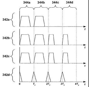
For example, referring to FIG. 3C, graphs 342a-d
are shown of signals that may result from use of the
process 500. As described above with respect to FIG.
3B, the horizontal axes of graphs 342a-d represent time
and the vertical axes represent voltage. Graphs 342a
and 342b are graphs of the voltage drop across print
head elements 102a and 102b, respectively, over the
course of four print head cycles 344a-d. Assume for
purposes of example that print head element 102a is
active for print head cycles 344a-b and inactive for
print head cycles 344c-d. Further assume for purposes
of example that print head element 102b is active in
each of print head cycles 344a-d. Graph 342d represents
a periodic latch signal that is identical to the latch
signal 322b described above with respect to FIG. 3B.
Graph 342c represents a strobe signal that may be
used in conjunction with the process 500 to provide
power to the print head elements 102a-b for the
appropriate amount of time tõ during each of the print
head cycles 344a-d. Consider, for example, print head
cycle 344a, during which both print head elements 102a-b
are active. The strobe signal remains TRUE for a
duration t, where n = 2. Since both print head elements
102a-b are active during print head cycle 344a,
25. corresponding graphs 342a-b indicate that power is
delivered to both print head elements 102a-b while the
strobe signal is TRUE. The same is true for print head
cycle 344b.
Turning to print head cycles 344c and 344d, only
print head element 102b (graph 342b) is active. As a
result, the voltage drop across print head element 102b
is higher than that of printhead cycles 344a and 344b.
CA 02476905 2004-08-19
WO 03/072362 PCT/US02/15473
28
The strobe signal remains TRUE during each of these
print head cycles for a duration t, where n = 1. As
indicated by graph 342c and because of the higher
voltage drop across 102b, the value of tn when n = 1, is
less than the value of t, when n = 2. Therefore, the
strobe signal remains TRUE for a shorter period of time
during each of print head cycles 344c-d than during
print head cycles 344a-b. As shown in graph 342b, print
head element 102b is therefore active for a shorter
period of time during each of print head cycles 344c-d
than during print head cycles 344a-b. It should be
appreciated that the constant amount of energy Eo may
therefore be provided to each of the print head elements
102a-b during each of the print head cycles 344a-d in
which each print head element is active.
It should be appreciated that the waveforms
illustrated in FIGS. 3A-3C are not drawn to scale and
are provided merely for purposes of example. For
example, the duration of each pulse of the strobe signal
illustrated in graph 342c of FIG. 3C is not necessarily
proportional to the corresponding value of tn. Rather,
the strobe signal illustrated in graph 342c is provided
merely to illustrate that the duration of the strobe
signal pulse decreases as the value of n decreases.
Examples of various techniques for selecting the
duration tõ (FIG. 5, step 506) are now described in more
detail. As mentioned above, the duration tn may be
selected so that the same amount of energy is delivered
to each active print head element during a particular
time interval (such as a print head cycle), regardless
of the number n of print head elements that are active
during that time interval.
CA 02476905 2004-08-19
WO 03/072362 PCT/US02/15473
29
Let Eo be the total amount of energy that is desired
to be output by each active print head element during a
print head cycle in order to produce a spot having a
desired density. If Po is the power delivered to each
active print head element when Ri is zero, and to is the
amount of time for which power Po must be delivered to a
print head element to produce energy Eo, then energy Eo
is shown in Equation 5:
Eo = Poto
Equation 5
Since Po is equal to V02/R when Ri is zero, Equation
5 can be rewritten as Equation 6:
2
Eo R to
Equation 6
Let Pn refer to the amount of power that is
delivered to a single active print head element when n
print head elements are contemporaneously active. Pn is
therefore given by Equation 7:
yoZ
P nR'Z
R
(1+ R
Equation 7
As can be seen from Equation 7, Pn decreases as the
number n of contemporaneously active print head elements
increases. If tn is the amount of time for which power
is delivered to n contemporaneously active print head
elements during a print head cycle, then the total
amount of energy En produced by each of the n print head
CA 02476905 2004-08-19
WO 03/072362 PCT/US02/15473
elements during the print head cycle is shown by
Equation 8:
E = P t,
Equation 8
5 In one embodiment of the present inventiori, the
time tõ is chosen during each print head cycle so that
the total amount of energy En produced during a print
head cycle by each of the n active print head elements
is equal to the desired amount of energy Eo, as shown in
10 Equation 9:
En = EO
Equation 9
In other words, the time tõ may be selected so that
En does not vary from print head cycle to print head
15 cycle, regardless of changes in the value of n (the
number of active print head elements) from print head
cycle to print head cycle. Therefore, if time tõ is
selected so that Equation 9 is satisfied, then the
desired amount of energy Eo may be output by each active
20 print head element during each print head cycle
regardless of the number n of contemporaneously active
print head elements by providing power to each print'
head element for time t,,.
Substituting in values of En and Eo into Equation 9
25 leads to Equation 10:
V2 _ V2
Rr 1+~p1 Z tn R to
~ Rl
Equation 10
Solving for tõ gives Equation 11:
CA 02476905 2004-08-19
WO 03/072362 PCT/US02/15473
31
z
tõ=11+ R) to
Equation 11
As described above with respect to FIG. 5, in one
embodiment of the present invention, the desired amount
of energy Eo is delivered by each of n active print head
elements during a particular print head cycle by
selecting a value of tn (step 506) and providing power Pn
to each of the n active print head elements for time tn
by making the strobe signal TRUE for time tõ (step 508)
It should be appreciated that the value of tn may, for
example, be calculated in step 506 using Equation 11.
Such a calculation may use as its inputs the values of
n, to, Ri, and R. The calculation may, for example, use
the ratio Ri/R as an input instead of the individual
values of Ri and R.
Although step 506 (FIG. 5) may be implemented by
calculating the duration tõ on the fly (i.e., as the
process 500 is being performed), such as by using
Equation 11, above, this is not a limitation of the
present invention. Rather, the duration tn may be
calculated, generated, or selected in any of a variety
of ways. Approximations to Equation 11 may be used if,
for example, faster calculation of tn is desired. For
example, if the ratio NRi/R is very small (e.g. less than
0.1), where N is the maximum number of print head
elements that may be active in a single print head
cycle, then the term (nRi/R)2 in the expansion of
Equation 11 may be ignored, in which case Equation 11
may be approximated by Equation 12:
CA 02476905 2004-08-19
WO 03/072362 PCT/US02/15473
32
rn=11+2)ro
Equation 12
For example, in one embodiment of the present
invention, the ratio Ri/R is approximately equal to 10-5,
in which case Equation 12 may advantageously by used to
calculate an approximation to tn.
Alternatively, a lookup table may be pre-generated
that contains values of tr, indexed by the number n. When
the value of n is determined (FIG. 5, step 504), the
corresponding value of tn may be obtained (step 506) by
looking it up in the lookup table. A smaller lookup
table containing fewer than all possible values of tn may
be used, and interpolation may be used to estimate
values of tn that are not stored in the lookup table, or,
the number, n, is scaled or bit-shifted so that it falls
within the range of the lookup table. Various
combinations of the techniques just described may also
be used.
Various embodiments described above employ the
following features: constant-duration print head cycles,
a periodic latch signal (such as the latch signal shown
in graph 342d) which rises at approximately the
beginning of each print head cycle, and a strobe signal
which rises at approximately the beginning of each print
head cycle and remains high for time t,,. These
particular features, however, are provided merely for
purposes of example and do not constitute limitations of
the present invention. For example, the features just
described result in "dead time" between strobe signal
CA 02476905 2004-08-19
WO 03/072362 PCT/US02/15473
33
pulses (as illustrated by the gaps between pulses of the
strobe signal in graph 342c).
In one embodiment of the present invention, this
"dead time" is eliminated by collapsing the strobe
signal pulses so that each pulse of the strobe signal
commences immediately after the preceding strobe signal
pulse terminates. This may effectively produce one
continuous-strobe signal. Furthermore, a non-periodic
latch signal is used in which the peak of each latch
signal pulse is timed to substantially coincide with the
initiation of a corresponding strobe signal pulse. The
"dead time" between strobe signal pulses and between
print head element "on" times may therefore be
substantially or entirely eliminated. In this
embodiment, the duration of the "on time" (tn)for each
print head element is still a function of the number of
contemporaneously-active print head elements, and the
value of t, for each print head element may be calculated
in the same manner as described above. Those of
ordinary skill in the art will appreciate how to
implement this embodiment using the techniques described
elsewhere herein.
As described above with respect to Equation 11, tn
is a function of time to. The value of to may be chosen
in any of a variety of ways. In one embodiment of the
present invention, power is delivered to each active
print head element during a portion of a print head
cycle. In this embodiment, therefore, it is desired
that tn not exceed T,, the duration of a print head
cycle, for any value of n. If N is the maximum number
of print head elements that may be active in a single
CA 02476905 2004-08-19
WO 03/072362 PCT/US02/15473
34
print head cycle, then the desired relationship between
tN and T, is shown by Equation 13:
tN<_T,
Equation 13
As seen from Equation 11, tn = f(n) t0, where the
value of f(n) is as shown in Equation 14:
.f 1 Z
(n) + nR.
R
J
Equation 14
Based on Equation 14, the value of tN may be
obtained by letting n.= N in Equation 11, resulting in:
tN-J\"Jt0
Equation 15
Solving for to leads to Equation 16:
to = ktN
Equation 16
where k = l/f(N), as expanded in Equation 17:
k = 1 ~
~1+ RJ
Equation 17
The value k is referred to herein as a "correction
factor." By using Equation 13, we can rewrite Equation
16 as Equation 18:
to<_kT
Equation 18
Therefore, in one embodiment of the present
invention, a value of to is chosen so that to satisfies
CA 02476905 2004-08-19
WO 03/072362 PCT/US02/15473
Equation 18. This may be accomplished by: (1)
calculating, estimating, or otherwise selecting a value
of k based on the known values of N and R;,/R, (2)
selecting kT, based on the known values of k and T,, and
5 (3) selecting a value of to that is less than or equal to
kT,, thereby satisfying Equation 18.
In one embodiment, the value of the NRi/R term in
Equation 18 is approximately equal to 0.1. This results
in a value of k approximately equal to 0.826. If T, is
10 equal to 1/300th of a second (approximately 0.00333),
then kT, is approximately equal to 0.00275 seconds. Any
value for to that is less than 0.00275 seconds may
therefore be chosen to satisfy Equation 13, thereby
ensuring that power will not be delivered to any print
15 head element for longer than the duration of a print
head cycle regardless of the number n of print head
elements that are active during the print head cycle.
It should be appreciated that the techniques just
described for selecting a value of to are provided merely
20 for purposes of example and do not constitute a
limitation of the present irivention. Rather, the value
of to may be chosen in other ways that fall within the
scope of the claims.
As described above, tn may be calculated from the
25 values of n, to, Ri, and R using Equation 11. Examples
of techniques for obtaining values of n and to are
described above. All that remains for purposes of
calculating t, is to obtain values of Ri and R or to
obtain a value for the ratio Ri/R, referred to herein as
30 r. Examples of techniques for obtaining values of Ri, R,
and the ratio r are now described in more detail.
CA 02476905 2004-08-19
WO 03/072362 PCT/US02/15473
36
In one embodiment of the present invention, the
values of Ri and R are measured in the circuitry 200
using standard techniques or are previously known based
on knowledge of the circuitry 200. The ratio r may then
be readily ascertained by dividing Ri by R.
Calculation of tn using Equation 11, however, does
not require that the individual values of Rj and R be
known, so long as the ratio Ri/R is known. Recalling
that r is the ratio Ri/R, Equation 11 may be rewritten as
Equation 19:
t,, -f" YIY)Z t0
Equation 19
In one embodiment of the present invention, the
value of r or an approximation thereto is developed
using a target rendered on an output medium. The target
may be visually inspected and the value of r may be
derived from observations made during the visual
inspection.
More specifically, referring to FIG. 6A, a source
target 600 is shown according to one embodiment of the
present invention. The source target 600 is a digital
image that may be stored, for example, in a computer-
readable memory such as a Random Access Memory (RAM) or
in a file on a hard disk drive. The source target 600
therefore includes a two-dimensional array of pixels.
In one embodiment of the present invention, the target
600 is a grayscale image, in which case the digital
value of each pixel in the target 600 specifies a level
of gray. For example, if the target 600 is an 8-bit
grayscale image, then each pixel may have a grayscale
value ranging from 0 to 255.
CA 02476905 2004-08-19
WO 03/072362 PCT/US02/15473
37
The cross-hatch pattern used to illustrate the
target 600 in FIG. 6A represents a particular level of
gray, such as a grayscale value of 128 out of 255. As
shown in FIG. 6A, all pixels of the striped bars of the
source target 600 have the same digital value,
specifying a single shade of gray. As described in more
detail below, however, all pixels of target 600 may not
appear to be the same shade of gray when the source
target 600 is rendered on an output medium as an output
target by a thermal printer. Rather, some pixels may
appear darker or lighter than others. The source target
600 shown in FIG. 6A, however, is illustrated using a
single shade of gray to indicate that the source target
600 is a digital image in which all pixels have the same
digital value.
The source target 600 includes a long, narrow bar
602 down the center, with a series of horizontal bars
604a-m flanking the vertical bar 602. The vertical bar
602 and each of the horizontal bars 604a-m is a two-
dimensional array of pixels. The bars 602 and 604a-m
may be of any width and height, but should at least be
large enough to be clearly visible to the human eye when
rendered on an output medium. Furthermore, the rendered
appearance of the source target 600 that is
advantageously used in the method described below with
respect to FIG. 8 is more pronounced if the horizontal-
bars 604a-m are substantially wider than (and therefore
include many more pixels in each row than) the vertical
bar.
As described above, the target source 600 is a
digital image. In one embodiment of the present
invention, the source target 600 is rendered on an
CA 02476905 2004-08-19
WO 03/072362 PCT/US02/15473
38
output medium as an output target by a thermal printer
using a process 700 shown in FIG. 7A. For purposes of
example, FIG. 6A is oriented with its vertical axis
being parallel to a slow scan direction of the thermal
printer. As a result, horizontally-adjacent pixels in
the source target 600 are rendered by different print
head elements. The process 700 begins by setting the
value of a variable named DutyCycle to 100 (step 702).
As shown in FIG. 6A, the target 600 includes a
series of horizontal segments 610a-f. The horizontal
segments 610a-f contain first portions 606a-f and second
portions 608a-f. For example, horizontal segment 610a
includes: (1) a first portion 606a including two
horizontal bars 604a-b and a portion 602a of the
vertical bar 602 located between the two horizontal bars
604a-b, and (2) a second portion 608a including a
portion 602b of the vertical bar 602 that is not between
the two horizontal bars 604a-b. The remaining
horizontal segments 610b-f contain similar first and
second portions (which are not separately labeled in
FIG. 6A for ease of illustration).
The process 700 enters a loop over each horizontal
segment H in the source target 600. The first portion
of the horizontal segment H is printed with a
predetermined duty cycle, such as 100% (step 706). As
used herein, the term "duty cycle" refers to the amount
of time that a heating element is activated in order to
print a spot relative to the time of a single print head
cycle. This can be expressed as:
duty cycle = Tt C
CA 02476905 2004-08-19
WO 03/072362 PCT/US02/15473
39
A duty cycle may, for example, be expressed as a
percentage of a print head cycle. For example, a duty
cycle of 100o refers to the entire duration of a print
head cycle. Therefore, in step 706, active print head
elements are activated for 1000 of each print head cycle
when printing the first portion of horizontal segment H.
The second portion of the horizontal segment H
(i.e., the portion not containing horizontal bars) is
printed with a duty cycle equal to DutyCycle (step 708).
The value of DutyCycle is decreased by 5%, or some other
predetermined value (step 710). As a result, the second
portions 608a-f of the source target 600 are printed
using decreasing duty cycles going down the target 600.
Steps 706-710 are repeated for the remaining horizontal
segments in the source target 600 (step 712). Referring
to FIG. 6B, an output target 620 is shown as it might
appear on an output medium when rendered by a thermal
printer using the process 700.
Returning for a moment to FIG. 6A, it can be seen
that there are many more gray pixels in each row of the
first horizontal portions 606a-f than in each row of the
second horizontal portions 608a-f. As a result, more
print head elements will be contemporaneously active
when the first portions 606a-f are being printed than
when the second portions 608a-f are being printed.
Therefore, based on the discussion above, it is to be
expected that each of the first portions 606a-f will,
when printed, have a lower pigment density, and
therefore appear lighter, than a corresponding one of'
the second portions 608a-f that is printed using the
same duty cycle.
CA 02476905 2004-08-19
WO 03/072362 PCT/US02/15473
The vertical bar 602 (FIG. 6A), when rendered on
the output medium, will appear to be a vertical bar 622
(FIG. 6B) consisting of alternating first squares 632a-f
and second squares 634a-f. The second squares 634a-f
5 appear successively lighter moving from the top to the
bottom of the output target 620. For example, second
square 634c is lighter than second square 634b, which in
turn is lighter than second square 634a. Increasingly
light shades are represented by various cross-hatch
10 patterns in FIG. 6B. The increasing lightness of second
squares 634a-f is the result of using decreasing duty
cycles to print each successive second portion in the
process 700.
Now turn to first portions 626a-f of horizontal
15 segments 630a-f (FIG. 6B), which are the result of
rendering first portions 606a-f of horizontal segments
610a-f (FIG. 6A). Although first portions 606a-f (FIG.
6A) were rendered using a 1000i duty cycle, corresponding
first portions 626a-f (FIG. 6B) appear lighter than
20 otherwise would have occurred where there was no common
voltage effect. The energy output of the print head
elements was correspondingly decreased according to
Equation 11, resulting in less dense (i.e., lighter)
output.
25 It should be appreciated that the roles of the
first portions 606a-f of horizontal segments 610a-f (FIG. 6A) can be exchanged
with second portions 608a-f.
More specifically, all second portions may be printed
with a fixed duty cycle that is less than 1000 (e.g.
30 80%), while first portions 606a-f may be printed with
duty cycles that step through predetermined cycles,
CA 02476905 2004-08-19
WO 03/072362 PCT/US02/15473
41
starting at duty cycle value of the second portions
608a-f and increasing toward 100%.
To find the value of r, one may visually inspect
the center bar 602, finding which of squares 634a-f (of
varying shades) match squares 632a-f (of constant shade)
using a process described below. A sufficiently good
match is found when one cannot perceive a difference in
shade between adjacent squares. If no match is found,
one may estimate a new starting value for DutyCycle in
process 700 and a refined step size for changing it in
step 710.
Finding a visual match between adjacent squares
indicates that the adjacent squares were printed with
the same energy per pulse. Using Equation 7 and Equation
8, we can write this equality as:
Vz _ VZ
R(1 + nr)2 ft R(1 + Nr)2 t
Equation 20
Here, n is the number of contemporaneously active
elements in second squares 634a-f, N is the number of
contemporaneously active elements in first squares 632a-
f, and f is the percent duty cycle for the matching
square expressed as a fraction. Solving Equation 20 for
r yields:
r- (1-yJ )
(JN - n)
Equation 21
It should be appreciated that if the roles of the
squares 632a-f and 634a-f are exchanged as described
above, then Equation 21 will need to be changed in a
CA 02476905 2004-08-19
WO 03/072362 PCT/US02/15473
42
manner that will be apparent to those of ordinary skill
in the art.
Another technique for rendering the source target
600 will now be described. In another embodiment of the
present invention, the source target 600 is rendered on
an output medium as an output target by a thermal
printer using a process 720 shown in FIG. 7B. The
process 720 is similar to the process 700, except that
it varies the duty cycle used to print the horizontal
segments 630a-f by varying the value of r, rather than
by directly varying the duty cycle.
More specifically, the process 720.begins by
setting the value of r to a maximum value MAX (step
722). The value MAX may be chosen in any manner, but
should be selected to be greater than the maximum value
expected for r based on any pre-existing knowledge of
the circuitry 200. Using this maximum value of r plus
knowledge of the number of print head elements, N, the
time for a print head cycle, T, and Equations 17 and 18,
a value for to is computed for use in the process. The
process 720 enters a loop over each horizontal segment H
in the source target 600. Both portions of the
horizontal segment H are printed with duty cycles that
are based on the known values of n and 'to and the current
value of r (steps 726 and 728). The duration tn of the
duty cycle may, for example, be calculated using
Equation 11, as described above. The value of r is
decreased by a predetermined value INC, which may be
selected in any manner (step 730). The value INC may be
selected, for example, so that the values of r used to
print the horizontal segments 630a-f span a range of
values for r that is likely to include an optimal value
CA 02476905 2004-08-19
WO 03/072362 PCT/US02/15473
43
for r. Steps 726-730 are repeated for the remaining
horizontal segments in the source target 600 (step 732).
The output target generated by the process 720 will be
substantially similar to the output target 620 shown in
FIG. 6B, although the specific darknesses (gray levels)
of both the first and second portions of 630a-f rendered
by processes 700 and 720 may not be the same.
Referring to FIG. 8, in one embodiment of the
present invention, characteristics of the output target
620 may be used to estimate the ratio r (used by
Equation 11) using a process 800. The output target 620
is rendered, such as by the process 700 (FIG. 7A) or by
the process 720 (FIG. 7B) described above (step 802). A
second square in the output target 620 is identified
whose tone (e.g., blackness) most closely matches the
tone of the first squares 632a-f (step 804). This
identification may be performed, for example, by
visually inspecting the output target 620 and
identifying the second square whose tone appears to
match the tone of the first squares 632a-f most closely.
The arrangement of the first squares 632a-f and the
second squares 634a-f in the output target 620 may be
used to facilitate this identification by visual
inspection. Note, for example, that at the top of
output target 620, first square 632a is lighter than
corresponding second square 634a, which is very dark.
Turning to the bottom of output target 620, the
situation is reversed: first square 632f is darker than
second square 634f. Since second squares 634a-f are
successively lighter moving from the top to the bottom
of output target 620, there should be a second square
having a blackness that matches the blackness of the
CA 02476905 2004-08-19
WO 03/072362 PCT/US02/15473
44
first squares more closely than any other second square.
The arrangement of first squares 632a-f and second
squares 634a-f facilitates the visual identification of
this second square. The viewer may, for example, begin
by inspecting and comparing the darkness of the second
square 634a at the top of the output target 620 to the
blacknesses of the first squares 632a and 632b
immediately above and below it. The viewer may continue
by moving down the output target 620 and comparing the
blackness of each of the second squares 634a-f to that
of the first squares above and below it, until a second
square having a blackness that most closely matches the
blackness of the first squares 632a-f is identified.
The uniform blackness of the first squares 632a-f (which
serves as a reference point against which the
blacknesses of the second squares 634a-f may be
compared), the decreasing blackness of the second
squares 634a-f, and the physical proximity of the second
squares 634a-f to the first squares 632a-f facilitates
' the process of selecting a second square whose blackness
most closely matches that of the first squares 632a-f.
Once a second square has been identified (such as
by using the techniques just described), a value of r is
selected based on the identified second square (step
806). For example, if the output target 620 was
rendered by the process 720 (FIG. 7B), then the value of
r that was used to print the identified second square is
a known value (see step 728). Therefore, step 806 may
be performed by identifying the value of r that was used
in step 728 of process 720 to print the second square.
Assume, for example, that second squares 634a-f are
numbered sequentially beginning with zero (e.g., second
CA 02476905 2004-08-19
WO 03/072362 PCT/US02/15473
square 634a is square zero, second square 634b is square
one, etc.). Then, if square number m is identified in
step 804, the corresponding value of r selected in step
806 is equal to MAX - (m X INC) (where MAX and INC are
5 the values used by process 720).
FIGS. 6A and 6B show specific examples of a source
target 600 and an output target 620, respectively. It
should be appreciated, however, that these targets 600
and 620 are shown and described merely for purposes of
10 example and do not constitute limitations of the present
invention. Rather a variety of other targets that may
be used to select a value of r are within the scope of
the claims.
More generally, source and output targets that may
15 be used in various embodiments of the present invention
have the following features. In general, a source
target (e.g., source target 600) is a digital image that
may be rendered on an output medium as an output target
(e.g., output target 620). The source target includes a
20 first plurality of source regions (e.g., the first
portions 606a-f) having a predetermined digital value.
Pixels in the first plurality of source regions are
arranged so that a first predetermined number of heating
elements are active when the first plurality of source
25 regions are rendered on the output medium as a first
plurality of output regions (e.g., the first portions
626a-f). The first plurality of source regions are
rendered on the output medium using a constant duty
cycle (e.g., as described with respect to steps 706 and
30 726 above). Because pixels in the first plurality of
source regions have the same predetermined digital
value, are rendered using the same number of active
CA 02476905 2004-08-19
WO 03/072362 PCT/US02/15473
46
heating elements, and are rendered using the same duty
cycle, the plurality of output regions will have a
constant blackness that may serve as a visual reference
point.
The source target also includes a second plurality
of source regions (e.g., second portions 608a-f) also
having the predetermined digital value. Pixels in the
second plurality of source regions are arranged so that
a second predetermined number of heating elements are
active when the second plurality of source regions are
rendered on the output medium as a second plurality of
output regions. The second plurality of source regions
are rendered on the output medium using a plurality of
duty cycles (e.g., as described above with respect to
steps 708 and 728). Because the second plurality of
source regions have the same predetermined digital value
and are rendered using the same number of active heating
elements, but are rendered using a plurality of duty
cycles, the second plurality of output regions will have
different blacknesses.
The first and second predetermined numbers of
heating elements are chosen to be unequal. For example,
in one embodiment of the present invention, the first
predetermined number of heating elements (i.e., the
number of heating elements that are active when
rendering the first plurality of source regions) is
chosen to be substantially larger than the second
predetermined number of heating elements (i.e., the
number of heating elements that are active when
rendering the second plurality of source regions).
In addition, the predetermined number of heating
elements in regions 604a-m do not necessarily need to be
CA 02476905 2004-08-19
WO 03/072362 PCT/US02/15473
47
the same. Using different numbers of heating elements
would, for instance, facilitate using processes 700 or
720 with a lookup table approach.
The output target may be visually inspected to
identify one of the second plurality of output regions
whose blackness most closely matches the blackness of
the first plurality of output regions (e.g., as
described above with respect to step 804). The second
plurality of output regions may be located near the
first plurality of output regions to facilitate such
identification. The ratio r may be determined based on
the selected one of the second plurality of output
regions, as described in more detail above with respect
to the particular embodiments described.
Although in the examples described above the first
portions 606a-f are rendered using a constant duty cycle
and the second portions 608a-f are rendered using a
varying duty cycle, the situation may be reversed. In
other words, the first portions 606a-f may be rendered
using a varying duty cycle and the second portions may
be rendered using a constant duty cycle.
Furthermore, although the examples above are
described with respect to a grayscale source and output
target, this is not a limitation of the present
invention. Rather the source and output targets may be
color images, in which case the term "tone" may be
substituted for "blackness" in the description of the
source and output targets above.
It should be appreciated that the various features
of embodiments of the present invention described above
and described in more detail below provide numerous
advantages.
CA 02476905 2004-08-19
WO 03/072362 PCT/US02/15473
48
By making constant the amount of energy delivered
by each active print head element to the output medium
during each print head cycle, various embodiments of the
present invention may be used to render output having
tones (e.g., gray levels) that more accurately represent
the tones in the source image being rendered. Because
the energy output by an active print head element in a
particular print head cycle is independent of the number
of print head elements that are active during the print
head cycle, various embodiments of the present invention
avoid undesirable variations in output based on the
number of contemporaneously active print head elements.
Various embodiments of the source and output
targets described above may be advantageously used to
select the ratio r by a simple process of visual
inspection. As described above, the output target may
be visually inspected and a value of r may be obtained
based on the inspector's visual identification of two
regions in the target whose tone matches most closely.
This technique may be applied quickly and without the
need to perform mechanical or electrical tests on the
hardware of the thermal printer, further simplifying the
process while still obtaining accurate results.
As described above, some existing systems attempt
to compensate for decreased energy output when many
print head elements are active by increasing the gray
level of pixels being printed when many print head
elements are contemporaneously active. The gray level
of a pixel is typically increased by printing more spots
for each pixel, i.e., by activating the corresponding
print head for a greater number of print head cycles.
This technique may, however, interfere or be
CA 02476905 2004-08-19
WO 03/072362 PCT/US02/15473
49
inconsistent with other techniques used by thermal
printers. For example, there is a limit to the number
of print head elements that may be active during a
particular print head cycle in some thermal printers.
As a result, a technique referred to as "pixel
alternation" is sometimes used by thermal printers to
print digital images. Using this technique, disjoint
subsets of the print head elements are allowed to be
active during each successive print head cycle in a
round-robin fashion. Each subset contains no greater
than the maximum number of allowed print head elements,
thereby satisfying the above-stated requirement.
The technique above, in which the gray levels of
pixels are increased by printing additional spots for
each pixel, may interfere with pixel alternation
techniques by requiring that a print head element be
active during a particular print head cycle even though
that print head element is not in the designated subset
of print head elements for that print head cycle.
In contrast, various embodiments of the present
invention may be used in conjunction with any
combination of active print head elements during a
particular print head cycle or across print head cycles.
Such embodiments may, therefore, work in conjunction
with pixel alternation techniques, in combination with
any variety of halftone patterns, and more generally in
combination with any pattern of pixels. Such
embodiments may therefore be advantageously used to
improve print output quality without interfering with a
wide variety of other techniques conventionally used in
thermal printers.
CA 02476905 2004-08-19
WO 03/072362 PCT/US02/15473
The present invention has been described above in
terms of various embodiments. Various other
embodiments, including but not limited to the following,
are also within the scope of the claims.
5 Although the print head element resistors 208a-d
are shown and described above as having the same
resistance R, it should be appreciated that this does
not constitute a limitation of the present invention.
Rather, the print head element resistors 208a-d may have
10 different resistances, in which case the calculations
described above may be modified appropriately as will be
apparent to those of ordinary skill in the art.
Although some embodiments may be described herein
with respect to bilevel thermal printers, it should be
15 appreciated that this is not a limitation of the present
invention. Rather, the techniques described above may
be applied to printers other than thermal printers, and
to printers other than bilevels printers.
Although various embodiments are described herein
20 -with respect to the print head circuitry 200, this is
purely for purposes of example and does not constitute a
limitation of the present invention. Rather, the
techniques described herein may be applied to devices
other than thermal printers that include circuitry whose
25 structure is similar to the circuitry 200 shown in FIG.
2.
Various examples described above refer to print
head elements that are contemporaneously active during a
particular print head cycle. It should be appreciated,
30 however, that the techniques described herein may be
used to apply a desired amount of power to a particular
number of print head elements or other circuit
CA 02476905 2004-08-19
WO 03/072362 PCT/US02/15473
51
components during any time interval. Although a single
print head cycle is used as an example of such a time
interval in various parts of the description herein,
this is not a limitation of the present invention.
Rather, the time interval may be longer or shorter than
a print head cycle.
In general, the techniques described above may be
implemented, for example, in hardware, software,
firmware, or any combination thereof. The techniques
described above may be implemented in one or more
computer programs executing on a programmable computer
and/or printer including a processor, a storage medium
readable by the processor (including, for example,
volatile and non-volatile memory and/or storage
elements), at least one input device, and at least one
output device. Program code may be applied to data
entered using the input device to perform the functions
described herein and to generate output information.
The output information may be applied to one or more
output devices.
Printers suitable for use with various embodiments
of the present invention typically include a print
engine and a printer controller. The printer controller
receives print data from a host computer and generates
page information, such as a logical halftone to be
printed based on the print data. The printer controller
transmits the page information to the print engine to be
printed. The print engine performs the physical
printing of the image specified by the page information
on the output medium.
Elements and components described herein may.be
further divided into additional components or joined
CA 02476905 2004-08-19
WO 03/072362 PCT/US02/15473
52
together to form fewer components for performing the
same functions.
Each computer program within the scope of the
claims below may be implemented in any programming
language, such as assembly language, machine language, a
high-level procedural programming language, or an
object-oriented programming language. The programming
language may be a compiled or interpreted programming
language.
Each computer program may be implemented in a
computer program product tangibly embodied in a machine-
readable storage device for execution by a computer
processor. Method steps of the invention may be
performed by a computer processor executing a program
tangibly embodied on a computer-readable medium to
perform functions of the invention by operating on input
and generating output.
It is to be understood that although the invention
has been described above in terms of particular
embodiments, the foregoing embodiments are provided as
illustrative only, and do not limit or define the scope
of the invention. Other embodiments are also within the
scope of the present invention, which is defined by the
scope of the claims below. Other embodiments that fall
within the scope of the following claims include, but
are not limited to, the following.