Note: Descriptions are shown in the official language in which they were submitted.
CA 02477048 2004-08-20
WO 03/073314 PCT/US03/05135
METHOD AND SYSTEM FOR INTEGRATING CORES IN FPGA-BASED
SYSTEM-ON-CHIP (SoC)
FIELD OF THE INVENTION
This invention relates generally to programmable logic
devices, and more particularly to a method and system for
integrating cores for customizing FPGA-based SoCs.
BACKGROUND OF THE INVENTION
Programmable devices are a class of general-purpose
integrated circuits that can be configured for a wide
variety of applications. Such programmable devices have
two basic versions, mask programmable devices, which are
programmed only by a manufacturer, and field programmable
devices, which are programmable by the end user. In
addition, programmable devices can be further categorized
as programmable memory devices or programmable logic
devices. Programmable memory devices include programmable
read only memory (PROM), erasable programmable read only
memory (EPROM) and electronically erasable programmable
read only memory (EEPROM). Programmable logic devices
include programmable logic array (PLA) devices,
programmable array logic (PAL) devices, erasable
programmable logic devices (EPLD) devices, and programmable
gate arrays (PISA).
As chip capacity continues to increase significantly; the
use of field programmable gate arrays (FPGAs) is quickly
replacing the use of application specific integrated
circuits (ASICs). An ASIC is a specialized integrated
circuit that is designed for a particular application and
can be implemented as a specialized microprocessor.
Notably, a FPGA is a programmable logic device (PLD) that
has an extremely high density of electronic gates as
compared to an ASIC. This high gate density has
contributed immensely to the popularity of FPGAs. Notably,
FPGAs can be designed using a variety of architectures that
can include user configurable input/output blocks (IOBs),
and programmable logic blocks having configurable
interconnects and switching capability.
1
CA 02477048 2004-08-20
WO 03/073314 PCT/US03/05135
The advancement of computer chip technology has also
resulted in the development of embedded processors and
Controllers. An embedded processor or controller can be a
microprocessor or microCOntroller circuitry that has been
integrated into an electronic device as opposed to being
built as a standalone module or "plugin card." Advancement
of FPGA technology has led to the development of FPGA-based
system-on-chips (SoC) including FPGA-based embedded
processor SoCs. A SoC is a fully functional product having
its electronic circuitry contained on a single chip. While
a microprocessor chip requires ancillary hardware
electronic components to process instructions, a SoC would
include all required ancillary electronics. For example, a
SoC for a cellular telephone can include a microprocessor,
encoder, decoder, digital signal processor (DSP), RAM and
ROM. It should be understood within contemplation of the
present invention that an FPGA-Based SoC does not
necessarily include a microprocessor or microcontroller.
For example, a SoC for a cellular telephone could also
include an encoder, decoder, digital signal processor
(DSP), RAM and ROM that rely on an external microprocessor.
It should also be understood herein that "FPGA-based
embedded processor SoCs" are a specific subset of FPGA-
based SoCs that would include their own processors.
In order for device manufacturers to develop FPGA-
based SoCs or FPGA-based embedded processor SoCs, it is
necessary for them to acquire intellectual property rights
for system components and/or related technologies that are
utilised to create the FPGA-based SoCs. These system
components and/or technologies are called cores or
Intellectual Property (IP) cores. An electronic file
containing system component information can typically be
used to represent the core. A device manufacturer will
generally acquire several cores that are integrated to
fabricate the SoC.
Notwithstanding advantages provided by using FPGA-
based SoCs, the development of these SoCs can be very
challenging. Although a vast proportion of cores are
commercially available, a significantly greater proportion
2
CA 02477048 2004-08-20
WO 03/073314 PCT/US03/05135
of cores are proprietary. Proprietary cores can be called
customer specific cores. Commercially available cores can
typically include standardized interfaces, which can
provide interconnectivity between system components from
various vendors. Customer specific cores can typically
include proprietary interfaces that do not readily
facilitate interconnectivity between system components from
other vendors. For example, customer specific cores can be
written in proprietary languages, which are completely
different from standardized languages. Since customer
specific cores do not readily facilitate interconnectivity
with other vendor's system components, integrating customer
specific cores during customization of an FPGA-based SoC
can be time consuming. This resulted in increased
development cost and greater time-to-market. Integration of
the cores can include simulating, modeling and debugging
the integrated cores in an operating environment.
Simulation and modeling can be a daunting task since it can
take hours if not days to simulate a few milliseconds of
real time operation. FPGA based embedded processor SoCs are
being introduced into the market, but there are no
solutions which allow users to customize the system, the
hardware cores, and the associated software nor is there a
system enabling a user to tradeoff a function which is
implemented in hardware (FPGA fabric) or software (running
on the embedded processor). It would be desirable to have
a method and system for better integrating cores during
customization of FPGA-based SoCs and that further overcome
the shortcomings described above.
SUMM~1R.Y OF THE INVENTION
The invention can provide a method for integrating
system component cores during customization of a FPGA-based
SoC. Subsequent to selecting a system component used for
customizing the FPGA-based SoC, parameters can be used to
configure the selected system component for use with the
FPGA-based SoC. The parameters used to configure the
selected system component can be propagated and used to
configure peer system components. Notably, other
3
CA 02477048 2004-08-20
WO 03/073314 PCT/US03/05135
parameters that are used to configure the peer system
component can also be propagated and used to configure the
selected system component. The parameters used to
configure the peer system components can be propagated to
subsequently selected system components that can be used to
configure the FPGA-based SoC. Selection of the system
components can also include the provision of an option for
selecting a hardware implementation or a software
implementation for customizing the FPGA-based SoC.
Additionally, the step of selecting the system component
can include selecting a system component from the group
consisting of a hardware core and a software core. The
invention can also provide an interface for integrating
hardware or software system component cores used for
customizing an FPGA-based SoC.
In a further aspect of the invention, an interface is
provided for integrating hardware system component cores
used for customizing an FPGA-based SoC. The interface can
include a slave connection circuitry communicatively
interfaced to a processor bus and a master connection
circuitry communicatively interfaced to the processor bus.
A multiplexer (MU.X) can facilitate selecting the slave
connection circuitry or the master connection circuitry in
order to provide communication between the processor bus
and a selected hardware system component core used for
customizing the FPGA-based SoC. The selected hardware
system component core can be either a proprietary customer
specific hardware core or a commercially available hardware
core.
In accordance with the inventive arrangements, the
interface can further include a direct memory access (DMA)
controller for providing direct access to a memory device.
A write buffer and a read buffer can provide temporary
storage of I/O data, which can be communicated between the
memory device and the selected hardware system component
core. An interrupt controller coupled to a multiplexer can
latch individual interrupt signals and provide a single
signal to a microprocessor indicating an interrupt
condition. The microprocessor then typically clears the
4
CA 02477048 2004-08-20
WO 03/073314 PCT/US03/05135
interrupt condition that is latched in the interrupt
controller after servicing the interrupt in a peripheral.
In yet a further aspect of the invention, a GUI for
integrating system component cores during customization of
a FPGA-based SoC is provided. The GUI can include a
selection object for selecting a system component core for
customizing the FPGA-based SoC. A configuration object can
facilitate configuration of selected system component core
and peer system components. A display object can be used
to facilitate display of parameters used by the
configuration object to configure selected system
components and peer system components. The configuration
object can further include a parameter distribution object
for distributing the parameters to subsequently selected
system component cores and peer system components. The
selection object can further include a dialog for selecting
hardware system component cores and software system
component cores.
BRIEF DESCRIPTION OF THE DRAWINGS
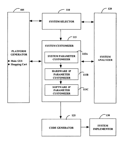
FIG. 1 is a block diagram of a processor system
generator in accordance with the invention.
FIG. 2 depicts an exemplary topological view of the
system model in accordance with the inventive arrangements.
FIG. 3 depicts a flow chart illustrating exemplary
steps for integrating system component cores in accordance
with the invention.
FIG. 4 depicts an interface for integrating software
system component cores in accordance with the inventive
arrangements.
FIG. 5 depicts an exemplary hardware interface for
integrating hardware system components in accordance with
the invention.
FIG. 6 depicts and exemplary GUI in accordance with
the present invention.
DETAILED DESCRIPTION OF THE DRAWINGS
Referring to FIG. 1, there is shown a block diagram
illustrating an exemplary system for developing and
5
CA 02477048 2004-08-20
WO 03/073314 PCT/US03/05135
verifying a FPGA-based SoC in accordance with the
invention. For illustrative purposes, and without limiting
the scope of the invention, an embedded system consisting
of a microprocessor, buses, memory architecture,
peripherals, and software components is presented, although
a system using an external microprocessor is certainly
contemplated within the scope of the invention. Exemplary
software components for the embedded system can include,
but is not limited to, device drivers and system software,
such as a real time operating system (RTOS) and protocol
stacks. An exemplary development environment for this
embedded system can include, but is not limited to, one or
more libraries for microprocessors, peripherals, system
software, and device drivers. The relevant bus
architectures and memory options that can be utilized for
the development of an FPGA-based SoC can be included in the
libraries. Further, a good example of hardware/software
function tradeoff can involve the protocol stack, which can
be implemented in either hardware or software. A user may
implement a protocol stack in software if there is
sufficient processing power to meet all performance
requirements or the user could implement the protocol stack
in hardware given sufficient FPGA resources and a presumed
need for higher performance.
In general, a system model can be created to
facilitate design and testing of an FPGA-based SoC. The
system model can include a data structure that represents
the internal structure and functionality of the FPGA-based
SoC. The system model can include, but is not limited to,
system components, interconnections between components, and
attributes, which define various characteristics and
functionality of the system components and
interconnections. The data structure can be a hierarchical
structure, for example a tree structure, which can mirror
the design hierarchy of the embedded system. This system
model can also include algorithms, which can facilitate
selection and customization of system components. Notably,
the system model can be part of an integrated object-
oriented system (OOS) that can facilitate selection and
6
CA 02477048 2004-08-20
WO 03/073314 PCT/US03/05135
customization of the system components. Alternatively,
other mechanisms and algorithms external to the system
model can facilitate selection and customization of the
system components.
Referring now to FIG. 1, there are shown a platform
generator 105, a system selector 110, a system customizer
115, a system analyzer 120, a code generator 125 and a
system implementor 130 all forming a processor system
generator. The platform generator 105 can include one or
more GUIs that can facilitate design of the system model.
A main GUI can provide various system options and
informational dialogs. The platform generator can include,
a navigator GUI having one or more dialogs and/or objects,
a topological GUI having one or more dialogs and/or objects
and a selection customizer GUI having one or more dialogs
and/or objects. One or more dialogs and/or objects can
provide system component resource counts, performance
estimates, power requirements and system and application
software requirements. For example, a GUI can be used to
display a table or chart representing the resource
allocation for the system components. Advantageously, such
table or chart can provide an easily readable condensed
view of the system resource allocation. An exemplary table
is illustrated below.
Device LUTs DFFs Slices BRAM =/Os
OPB Arbiter 300 200 200 0 9
UART 16450 500 400 300 0 12
Ethernet 10/100M 2500 1700 1500 0 12
Total Utilized 3300 2300 2000 0 21
Device Resources 122880 122880 61440 3456 1488
Available Resources 119580 120580 59440 3456 1267
Referring to the table, a condensed view of the system
resources is provided. Specifically, the table shows a
7
CA 02477048 2004-08-20
WO 03/073314 PCT/US03/05135
breakdown of particular resources utilized by each device
and also the total resources utilized by all devices. The
available resources can be computed based on the total
utilized resources and the total device resources. For
example, there are 122880 D-flip flops (DFFs) available.
OPB arbiter utilizes 200 DFFs, UAR.T 16450 utilizes 400
DFFs, and Ethernet 10/100M device utilizes 1700 DFFs.
Hence, there are 2300 DFFs utilized, which leaves 120580
available.
The navigator dialog and/or object can provide an
interactive interface that Can facilitate viewing of design
specification and configuration information. For example,
one or more navigator objects can provide a graphical view
to facilitate the insertion of a microprocessor from a
library into the system model. In a case where a universal
asynchronous receiver/transmitter (UART) is selected as a
peripheral, the navigator object and/or dialog can permit
customization of the UART. The navigator dialog can also
be configured to permit switching between multiple design
and implementation tasks. The topological dialog can
utilize a block diagram format to provide a topological
view that can visually represent the existing state of the
system model. The selection Customizer object can permit
the selection and customization of a system component.
Upon selection of a system component, a GUI which can
include a dialog and can facilitate Customization of the
system component. Platform generator 105 can have the
capability to permit a particular state and/or stage of the
system design and implementation to be saved and recalled
at a subsequent time.
System selector 110 can be a GUI that can facilitate
selection of the system components that can be used to
design the FPGA-based SoC. For example, the system
selector 110 can provide one or more dialogs that can
permit the selection of microprocessors, microcontrollers,
peripheral devices, buses, system software and application
software. During selection of system components, each of
the selected components can be independently treated.
8
CA 02477048 2004-08-20
WO 03/073314 PCT/US03/05135
The system Customizer 115 can include one or more GUIs
having objects and/or dialogs that can facilitate
customization or configuration of system components and
software. Referring to FIG. 1, there are shown a system
parameter customizer 115a, a hardware intellectual property
(IP) parameter Customizer 115b, and a software IP parameter
customizer 115c. The system parameter customizer 115a can
facilitate customization of the memory map, interrupt
bindings and priorities, and global and default system
parameter definitions. The hardware intellectual property
(IP) parameter customizer 115b can facilitate customization
of device specific parameters. For example, data bus
widths, IP interfaces and device specific parameters Can be
customized by hardware intellectual property (IP) parameter
Customizes 115b.
The software intellectual property (IP) parameter
customizes 115C can facilitate customization of software
specific parameters. For example, upon selection of a
system component or a peripheral, an interrupt request
(IRQ) number, a memory mapped I/O address and default
initialization parameters can be assigned to the peripheral
by the software IP parameter Customizes 115c. In a case
where a DART has been selected as a peripheral, default
parameters can include, but are not limited to, stop bits,
parity designation on/off, and baud rate. The Customizes
system 115 not only provides selection of the system
components, but can also be configured to bind system
parameters to system components. For example, the memory
map for a particular peripheral can be bound to the
peripheral giving the peripheral its unique memory address
space. Furthermore, a GUI having one or more dialogs can
be used to populate a system model data structure with
customization parameters and/or attributes.
The system analyzer 120 can include one or more GUIs
having objects and/or dialogs that can provide immediate
feedback regarding architectural choices made during
customization. The system analyzer 120 can include software
that can have the capability to validate and analyze the
system model while it is being customized. If problems
9
CA 02477048 2004-08-20
WO 03/073314 PCT/US03/05135
including, incompatibilities, conflicts and/or system
violations occur, the system analyzer 120 can issue
immediate warnings and/or provide possible solutions. The
system analyzer 120 can perform tasks such as system
checks, parameter consistency checks, data type and value
propagation checks, interconnection inference, and resource
and performance analysis. Interconnection reference
pertains to implications that can result from making
certain connections. The system analyzer 120 can also
assign device identifications (IDs) to system components
and computing configuration read-only-memory (ROM) data.
Exemplary system and parameter consistency checks can
include, matching data bus widths of peripherals and system
components, determining interrupt conflicts, determining
memory map conflicts, determining memory size and usage,
determining device counts, determining availability of FPGA
resources and determining maximum operating frequency.
The system analyzer 120 can be configured. to propagate
default values, global values and/or previously defined
values through the system model. For example, if a bus is
configured with a default data width of 16 bits, then each
peripheral that "sits on" or utilizes that bus can
automatically be configured with a data width of 16 bits.
It should be recognized by one skilled in the art that
although a peripheral device may be automatically
configured with the default bus width value, this value can
be overwritten. For example, depending on the application,
availability of certain devices can dictate that two (2) 8-
bit devices be utilized instead of a single 16-bit device.
Advantageously, the propagation of values can prevent
multiple entries of similar data which typically increases
development time.
During performance analysis, system analyzer 120 can
have the capability to determine if system components are
properly configured. For example, system analyzer 120 can
identify a high-speed device that has not been configured
with direct memory access (DMA). Since such a device can
invariably cause a system conflict, system analyzer can
consider it as a source of potential problem. System
CA 02477048 2004-08-20
WO 03/073314 PCT/US03/05135
analyzer 120 can also determine whether there are too many
devices residing on a bus based on the device count. For
example, the system analyzer 120 can have the capability to
determine whether there are too many high-speed devices on
a low speed bus. In this case, the system analyzer 120 can
indicate the possibility of errors and/or generate possible
solutions. By tracking memory usage, the system analyzer
120 can have the capability to determine whether the code
space assigned in the memory map is too large for the
physical memory. System analyzer 120 can also be
Configured to track physical resource requirements for
example, slice counts for IP blocks, and width and height
of specifications of IP blocks. A GUI can provide a visual
display of a resulting or representative floor plan to aid
with tracking and management of physical resources.
Code generator 125 can include one or more GUIs having
objects and/or dialogs that can facilitate generation of
the code necessary for implementing the design of the FPGA-
based embedded processor SoC or FPGA-based SoC. The code
necessary for implementing the design of the FPGA-based SoC
can be in a format such as the well known. hardware
description language (HDL). HDL is a language used to
describe the functions of an electronic circuit for
documentation, simulation and/or logic synthesis. Verilog
and VHSIC Hardware Description Language (VHDL) are
standardized HDLs which are well known by those skilled in
the art. Verilog and VHDL can be used to design electronic
systems at the component, board and system level. They can
facilitate the development of models at a very high level
of abstraction. Other formats now known or to be
discovered can also be used to represent the system model.
Depending on information generated by, for example,
the software IP parameter Customizes 115c, the code
generator 125 can tailor "header files," which can be used
to implement the software IP of the FPGA-based SoC.
Moreover, depending on the selected software IP,
processors, peripherals, operating system and device
drivers, code generator 125 can produce a source code
directory structure that can facilitate implementation of
11
CA 02477048 2004-08-20
WO 03/073314 PCT/US03/05135
the software IP of the FPGA-based SoC. The code generator
125 can also generate the necessary "make files," which are
files used to define the rules necessary for compiling and
building the code used to implement the software IP of the
FPGA-based SoC. The code generator 125 can be configured
to generate information that can be used for debugging.
The generated information can be in an ASCII format or
other suitable format and can include information such as
the memory map, the configuration ROM table and the
peripheral ID map.
The system implementor 130 can include one or more
GUIs that can have objects and/or dialogs that can
facilitate implementation of the FPGA-based SoC design.
Implementation of the design can include, but is not
limited to, HDL simulation and synthesis, mapping of
information generated by the code generator 125, placement,
routing and bitstream generation. An integrated tool or
separate tools can facilitate the implementation of the
FPGA-based SoC design.
FIG. 2 depicts an exemplary topological view of the
system model in accordance with the inventive arrangements.
A GUI 200 can facilitate display of the topological view
of the system model. GUI 200 can include a software
development window 205, a simulation model window 210 and a
core model window 215. The software development window 205
can include one or more objects representing the various
tools that can be used to create the code for the model
system. Software development window 205 can include a
compiler object 205a, an assembler object 205b, a linker
object 205c, a converter or formatter object 205d and a
SRAM object 205e. Software build tools such as compilers,
assemblers, linkers, and converters are well known by those
skilled in the art. Simulation model window 210 can
include an OPB toolkit object 210a, a DCR toolkit object
210b, a PLB toolkit object 210c, an SRAM model object 210d
and a SRAM model object 210e.
The core model window 215 can include objects
representing the system components that can comprise the
system model. Core model window 215 contains a 32-bit
12
CA 02477048 2004-08-20
WO 03/073314 PCT/US03/05135
peripheral bus 215a, a DCR bus 215b, a 64-bit processor
local bus 215c, a SDRAM controller 215d, a peripheral
controller 215e, a arbiter 215f, a processor core 2158, a
DMA. controller 215h, a PLB/0PB bridge 2151 and a serial
port 215j. A high level view of the interconnections
between the system components is shown in the core model
window 215. For example, PLB/OPB bridge 2151 provides
interconnections between buses 215a, 215b and 215c. Bus
215c facilitates communication between peripherals
including arbiter 215f, peripheral controller 215e, SDRAM
controller 215d, DMA controller 215h and processor core
2158. Arrows between the objects in the core model window
215 and the simulation model window 210 can illustrate a
relationship between corresponding objects in each model
window .
FIG. 3 depicts a flow chart illustrating exemplary
steps for integrating system component cores in accordance
with the invention. Referring to FIG. 3, in step 380,
system component #1 can be selected. System component #1
and any subsequently selected system component can include
a hardware core or a software core. In step 382, system
component #1 can be configured with parameters. In step
384, the system parameters can be propagated to make them
available for subsequently selected system components that
will utilize common parameters. In step 384, system
component #2 can be selected. In step 388, system
component #2 can be configured with parameters including
previously propagated common parameters. In step 400, any
new parameters that were used to configure system component ,
#2 can be propagated to make them available for previously
and subsequently selected system components that utilize
similar parameters.
It should be recognized by those skilled in the art
that the configuration and propagation of parameters can be
static or dynamic. Notably, as system components are
configured with new parameters, these new parameters are
propagated and made available for configuring other system
components. Importantly, these other system components can
include previously configured hardware and software system
13
CA 02477048 2004-08-20
WO 03/073314 PCT/US03/05135
components, as well as subsequently selected hardware and
software system components. Advantageously, the
propagation of system parameters can save on development
time, since it can obviate any need to re-enter similar
parameters which can be used to configure other selected
system components.
FIG. 4 depicts an interface 480, for integrating
software system component cores in accordance with the
inventive arrangements. Referring to FIG. 4, there are
shown an operating system layer 482, and operating system
adaptation layer 484 and a system component layer 486. The
operating system component layer 482 can facilitate
management of resources for the software system components
that are used to customize the FPGA-based SoC. The
operating system layer 482 can host an operating system
such as a RT~S.
The operating system adaptation layer 484 can
facilitate communication between. disparate system component
drivers, for example 486a, 486b 486c, and the operating
system layer 482. The system component drivers 486a, 486b
and 486c can be customer specific proprietary cores, each
having a different communication interface. Since each of
the component drivers 486a, 486b and 486c can have
different proprietary interfaces, communication messages
can be translated or converted to and from the proprietary
formats to facilitate communication with the operating
system layer 480. The operating system adaptation layer
484 can include a translator that can facilitate conversion
to and from the proprietary formats, so that information
can be communicated between the operating system layer 482
and the system component layer 486.
The system component layer 486 can include one or more
system component drivers. Each of the system component
drivers can be configured to handle the processing
functions for a system component. For example, system
component #1 driver can be configured to handle processing
functions for system component #1. For illustrative
purposes, system component #1 can represent serial device
215j. In this case, system component #1 driver 486a can be
14
CA 02477048 2004-08-20
WO 03/073314 PCT/US03/05135
used to process data in an associated data buffer for
serial device 215j. System component #1 driver 486 can
include an interrupt handling routine that can be used to
retrieve data pending in the associated data buffer for
serial device 215j.
FIG. 5 depicts an exemplary hardware interface for
integrating hardware system components in accordance with
the invention. Referring to FIG. 5, there is shown an
exemplary interface 500 that can facilitate integration of
variously configured peripheral system components that can
be utilized for configuring the FPGA-based SoC. The FPGA-
based SoC can be configured to utilize dedicated
transistors in the Silicon o~ the FPGA for implementing a
peripheral interface. Alternatively, the FPGA-based SoC
can be configured to utilize dedicated transistors in the
logic fabric of a FPGA for implementing a peripheral
interface. Importantly, the choice of peripheral
interfaces used for configuring the FPGA-based SoC can
affect resource utilization of the FPGA-based SoC. For
example, the resource utilization for a master-slave
peripheral interface implementation can be markedly
different from a slave only peripheral interface
implementation. Advantageously, the invention can provide
immediate feedback on system component and peripheral
selection and implementation during customization of the
FPGA-based SoC. Importantly, customization of the FPGA-
based SoC can occur under resource Constraints without the
need to spend expensive development time and effort.
Exemplary interface 500 can include, but is not
limited to, a multiplexer (MUX) 502, slave connection
circuitry 506, master connection circuitry 508, direct
memory access DMA) controller 510, interrupt controller
504, address decoder 514, write bufter 516, and read buffer
518. The MUX 502 can facilitate selection of the slave
connection circuitry 506 or the master connection
circuitry, which can be used to connect a proprietary or
customer specific or other hardware system component core
512 to processor bus 520. The interrupt controller 504
latches individual interrupt signals and provides an
CA 02477048 2004-08-20
WO 03/073314 PCT/US03/05135
indication of an interrupt condition to a processor (not
shown). DMA controller 510 can facilitate direct memory
access to a storage device such as a random access memory
(RAM). I/0 data transferred to and from the system
component core can be buffered in the write buffer 516 and
the read buffer 51~, which can both be selected by the MUX
502.
FIG. 6 depicts and exemplary GUI 350 that can
facilitate integrating system component cores during
customization of a FPGA-based SoC in accordance with the
invention. GUI 350 can include a system component
selection object 352, a parameter selection object 354 and
a display window 356. The system component selection
object 352 can facilitate selection of system components
that can be used to configure the FPGA-based SoC. System
component selection object 352 can include a window having
a plurality of system components that can readily be
selected. In other words, the selection object may
comprise a dialog for selecting hardware system component
cores and software system component cores. For example, a
radio button can be highlighted to select UART 16450 as a
system component for configuring the FPGA-based SoC.
Alternatively, one or more pull-down menus can be used to
facilitate the selection of system components by their
functionality. The system component selection object and
the parameter selection objection essentially form a
configuration object. The configuration object may further
comprise a parameter distribution object for distributing
the parameters to subsequently selected system component
cores and peer system components.
Parameter selection object 354 can include one or more
dialogs that can facilitate entry and or selection of
parameters that can be used to configure system components.
For example, system component UART 16550 can be configured
with parameter 354a that indicates the use of interrupt
request number 9 (IRQ9). The display window 356 can
include a window having one or more objects representing
allocation and use of resources.
16
CA 02477048 2004-08-20
WO 03/073314 PCT/US03/05135
Display window 356 can include one or more objects
that can display the allocation of system resources as the
system components are selected. A table object 362 can
provide a condensed view of the allocation, usage and
availability of the FPGA-based SoC resources. The table
object 362 illustrates exemplary resources, which can
include LUTS, DFFs, Slices, BRAMS, I/Os, Memory and
processor power. Specifically, the table object shows a
breakdown of particular resources utilized by each device
or system component and also the total resources utilized
by all the system components. The available resources can
be computed based on the total utilized resources and the
total device resources. For example, there are 122880 D-
flip flops (DFFs) available in the FPGA-based SoC. The
table object can also show the processing power required by
the system components. For example, the OPB arbiter
utilizes 0.2 DMIPs, UART 16550 utilizes 1.4 DMIPs, and
Ethernet 10/100M device utilizes ~.4 DMIPs. The total
processing power required for use by the system components
is 10 DMIPs. This leaves 290 DMIPs of the 300 DMIPS of the
FPGA-based SoC processing power resources for use by other
system components.
Customization is typically constrained by the
availability of FPGA-based SoC resources. For example, the
number of I/Os utilized by system components cannot exceed
the number of I/Os of the FPGA-based SoC. Advantageously,
the GUI 350 can provide real-time resource utilization
feedback during the selection and configuration stages of
the FPGA-based SoC development. By selecting a particular
system component, the resources utilized by that system
component can be immediately determined and displayed in
the GUI 350. The resources can be itemized in order to
simplify the tasks of selection and configuration of system
components. In one aspect of the invention, each system
component can have a corresponding application programming
interface (API) the can provide an exact or estimated
resource count.
Importantly, after all the system components have been
selected, a system analysis and consistency check can be
17
CA 02477048 2004-08-20
WO 03/073314 PCT/US03/05135
executed to ensure that the necessary system requirements
and specification are met. For example, since processing
delays can affect quality of service (QOS) in speech-based
telephony applications, it is pertinent to ensure that
processing delays caused by system components comply with
' the system specification and requirements. The system
analyzer 120 (FIG. 1) can traverse the selected components
and compute relevant resource allocation and usage
statistics. These statistics can be used to optimize the
allocation of system resources. System analyzer 120 can
also provide functions, which can have the capability to
determine system performance and power dissipation based on
system component selection and parameter configuration. The
GUI 350 can further include a message object 360 that can
facilitate display of warning messages, error messages,
inconsistency messages, and other types of messages and/or
information. System component selection object 352 shows
selected system components OPB arbiter, ethernet 10/100 and
UART 16550.
In another aspect of the invention, a chip support
package can be automatically created for the FPGA-based
SoC. Typically, board support packages (BSP) Can facilitate
hardware and software customization. A BSP can include a
circuit board and associated system and/or application
software. The system and application software can include
a collection of libraries, which typically isolate hardware
functionality of the circuit board from its software
functionality. For example, the BSP libraries can provide
software functions that can be used for hardware
initialization, interrupt handling, clock and timer
management, and data structures for memory mapping and
sizing. Nevertheless, a BSP usually correlates to a static
design of a specific circuit board with specific
components. A new circuit board with different components
.would then necessarily require a different BSP.
Advantageously, the FPGA-based SoC provides a more
flexible approach than the BSP, by locating system
components on a chip, in contrast to being on a separate
circuit board. Rather than hard-coding the initialization
18
CA 02477048 2004-08-20
WO 03/073314 PCT/US03/05135
of system components that reside on the circuit board of
the BSP, the FPGA-based SoC can permit initialization of
only those system components that are utilized for
customizing the FPGA-based SoC. This can drastically
reduce initialization time and save on often precious
memory. The code generator 125 and/or system implementor
130, can include a chip support package generator for
generating a chip support package (CSP) or a board support
package generator for generating a board support package
(BSP) once the system components used to customize the
FPGA-based SoC have been selected and configured. The code
generator and/or system implementor can serve as a tool to
automate the creation of a BSP based on a specific FPGA-
based SoC and a specific operating system to be integrated
with the hardware or software cores previously selected.
Advantageously, the ability to get real-time feedback
and resource allocation can provide optimal resource
allocation while configuring the system components used to
customize the FPGA-based SoC. Notably, this can
significantly reduce up-front development costs and non-
recurring engineering costs and ultimately reduces the time
to market. In light of the foregoing description of the
invention, it should be recognized that the present
invention can be realized in hardware, software, or a
combination of hardware and software. A method and system
for integrating cores during customization of an FPGA-based
SoC according to the present invention can be realized in a
centralized fashion in one computer system, or in a
distributed fashion where different elements are spread
across several interconnected computer systems. Any kind
of computer system, or other apparatus adapted for carrying
out the methods described herein, is suited. A typical
combination of hardware and software could be a general
purpose computer system with a computer program that, when
being loaded and executed, controls the computer system
such that it carries out the methods described herein.
The present invention can also be embedded in a
computer program product, which comprises all the features
enabling the implementation of the methods described
19
CA 02477048 2004-08-20
WO 03/073314 PCT/US03/05135
herein, and which, when loaded in a computer system, is
able to carry out these methods. Computer program or
application in the present context means any expression, in
any language, code or notation, of a set of instructions
intended to cause a system having an information processing
capability to perform a particular function either directly
or after either or both of the following a) conversion to
another language, code or notation; b) reproduction in a
different material form.
Additionally, the description above is intended by way
of example only and is not intended to limit the present
invention in any way, except as set forth in the following
claims.
2o