Note: Descriptions are shown in the official language in which they were submitted.
CA 02477310 2004-08-24
WO 03/071673 PCT/CA03/00257
-1-
Down Conversion Methodology and Topology Which Compensates
for Spurious Response
The present invention relates generally to communications, and more
specifically to a method and apparatus of demodulating RF (radio frequency)
signals
which compensates for spurious response. The preferred embodiment of the
invention satisfies the need for an inexpensive, high-performance, fully-
integrable,
multi-standard receiver.
Background of the Invention
Many communication systems modulate electromagnetic signals from
baseband to higher frequencies for transmission, and subsequently demodulate
those high frequencies back to their original frequency band when they reach
the
receiver. The original (or baseband) signal may be, for example: data, voice
or
video. These baseband signals may be produced by transducers such as
microphones or video cameras, may be computer generated, or may be transferred
from an electronic storage device. In general, the high frequencies provide
longer
range and higher capacity channels than baseband signals, and because high
frequency signals can effectively propagate through the air, they can be used
for
wireless transmissions as well as hard-wired or wave guided channels.
All of these signals are generally referred to as RF signals, which are
electromagnetic signals; that is, waveforms with electrical and magnetic
properties
within the electromagnetic spectrum normally associated with radio wave
propagation.
Wired communication systems which employ such modulation and
demodulation techniques include computer communication systems such as local
area networks (LANs), point-to-point communications, and wide area networks
(WANs) such as the Internet. These networks generally communicate data signals
over electrically conductive or optical fibre channels. Wireless communication
systems which may employ modulation and demodulation include those for public
broadcasting such as AM and FM radio, and UHF and VHF television. Private
communication systems may include cellular telephone networks, personal paging
devices, HF radio systems used by taxi services, microwave backbone networks,
interconnected appliances under the Bluetooth standard, and satellite
communications. Other wired and wireless systems which use RF modulation and
CA 02477310 2004-08-24
WO 03/071673 PCT/CA03/00257
-2-
demodulation would be known to those skilled in the art.
Most RF receivers use the "super-heterodyne" topology, which provides good
performance in a limited scope of applications, such as in public-broadcast FM
radio
receivers. As will be explained, the super-heterodynes design limitations make
its
use in more sophisticated modern applications expensive, and its performance
poor.
The super-heterodyne receiver uses a two-step frequency translation method
to convert an RF signal to a baseband signal. Figure 1 presents a block
diagram of
a typical super-heterodyne receiver 10. The mixers labelled M1 12 and M2 14
are
used to translate the RF signal to baseband or to some intermediate frequency
(IF).
The balance~of the components amplify the signal being processed and filter
noise
from it.
The RF band pass filter (BPF1 ) 18 first filters the signal coming from the
antenna 20 (note that this band pass filter 18 may also be a duplexer). A low
noise
amplifier 22 then amplifies the filtered antenna signal, increasing the
strength of the
RF signal and reducing the noise figure of the receiver 10. The signal is next
filtered
by another band pass filter (BPF2) 24 usually identified as an image rejection
filter.
The signal then enters mixer M1 12 which multiplies the signal from the image
rejection filter 24 with a periodic signal generated by the local oscillator
(L01 ) 26.
The mixer M1 12 receives the signal from the image rejection filter 24 and
translates
it to a lower frequency, known as the first intermediate frequency (IF1 ).
Generally, a mixer is a circuit or device that accepts as its input two
different
frequencies and presents at its output:
(a) a signal equal in frequency to the sum of the frequencies of the input
signals;
(b) a signal equal in frequency to the difference between the frequencies of
the
input signals; and
(c) the original input frequencies.
The typical embodiment of a mixer is a digital switch which may generate
significantly more tones than stated above.
The IF1 signal is next filtered by a band pass filter (BPF3) 28 typically
called
the channel filter, which is centred around the IF1 frequency, thus filtering
out the
unwanted products of the first mixing processes; signals (a) and (c) above.
This is
necessary to prevent these signals from interfering with the desired signal
when the
second mixing process is performed.
The signal is then amplified by an intermediate frequency amplifier (IFA) 30,
and is mixed with a second local oscillator signal using mixer M2 14 and local
CA 02477310 2004-08-24
WO 03/071673 PCT/CA03/00257
-3-
oscillator (LO2) 32. The second local oscillator L02 32 generates a periodic
signal
which is typically tuned to the IF1 frequency. Thus, the signal coming from
the
output of M2 14 is now at baseband, that is, the frequency at which the signal
was
originally generated. Noise is now filtered from the desired signal using the
low pass
filter LPF 38, and the signal is passed on to some manner of presentation,
processing or recording device. For example, in the case of a radio receiver,
this
might be an audio amplifier, while in the case of a computer modem this may be
an
analogue to digital convertor.
Note that the same process can be used to modulate or demodulate any
electrical signal from one frequency to another.
The main problems with the super-heterodyne design are:
~ it requires expensive off-chip components, particularly band pass filters
18,
24, 28, and low pass filter 38;
~ the off-chip components require design trade-offs that increase power
consumption and reduce system gain;
~ image rejection is limited by the off-chip components, not by the target
integration technology;
~ isolation from digital noise can be a problem; and
~ it is not fully integratable.
The band pass and low pass filters 18, 24, 28 and 38 used in super-
heterodyne systems must be high quality devices, so electronically tunable
filters
cannot be used. As well, the only way to use the super-heterodyne system in a
multi-standard/multi-frequency application is to use a separate set of off-
chip filters
for each frequency band.
Direct-conversion transceivers attempt to perform up and down conversion in
a single step, using one mixer and one local oscillator. In the case of down-
conversion to baseband, this requires a local oscillator (LO) with a frequency
equal
to that of the input RF signal. If the LO signal of a direct conversion
receiver leaks
into the signal path, it will also be demodulated to baseband along with the
input
signal, causing interference. This LO leakage problem limits the utility of
direct-
conversion transceivers.
One of the current problems in the art is to develop effective receivers that
can adapt to the varying requirements caused either by changing reception
conditions, or even changing standards during the use of the device. For
cellular
telephones and similar consumer items, it is desirable to have receivers that
can be
CA 02477310 2004-08-24
WO 03/071673 PCT/CA03/00257
-4-
fully integrated onto inexpensive, low power integrated circuits (ICs).
A continuing desire to implement lower-cost, more power-efficient receivers
has led to intensive research into the use of highly integrated designs; an
increasingly important aspect for portable systems, including cellular
telephone
handsets. This has proven especially challenging as the frequencies of
interest in
the wireless telecommunications industry (especially low-power cellular/micro-
cellular
voice/data personal communications systems) have risen above those used
previously (approximately 900 MHz) into the spectrum above 1 GHz.
However, none of the attempts made to date have met with much success.
Receiver designs which are highly integrated typically have significant noise
and
quality problems. As well, few make any attempt at all to address transient or
spurious noise problems.
Thus, there is a need for a method and apparatus for modulation and
demodulation which addresses the problems above. It is desirable that this
design
be fully-integratable, inexpensive and high performance. As well, it is
desirable that
this design be easily applied to multi-standard/multi-frequency applications.
Summary of the Invention
It is therefore an object of the invention to provide a novel method and
system of modulation and demodulation which obviates or mitigates at least one
of
the disadvantages of the prior art.
One aspect of the invention is defined as a demodulator circuit for emulating
the down conversion of an input signal x(t) with a local oscillator (LO)
signal, the
demodulator circuit comprising: a first mixer for receiving the input signal
x(t), and
mixing the input signal x(t) with a multi-tonal mixing signal cp1, to generate
an output
signal cp1 x(t); a second mixer for receiving the signal cp1 x(t) as an input,
and mixing
the signal cp1 x(t) with a mono-tonal mixing signal cp2, to generate an output
signal
cp1 cp2 x(t); a first signal generator for generating the multi-tonal mixing
signal cp1; a
second signal generator for generating the mono-tonal mixing signal cp2, where
cp1
cp2 has significant power at the frequency of the local oscillator signal
being
emulated; and a power measurement circuit for measuring the power of the
output
signal cp1 cp2 x(t); the second signal generator receiving a power level
signal output
from the power measurement circuit, and varying the characteristics of the
mono-
tonal mixing signal cp2 to reduce the power level of the output signal cp1 cp2
x(t).
Another aspect of the invention is defined as a method of emulating the
CA 02477310 2004-08-24
WO 03/071673 PCT/CA03/00257
-5-
demodulation of an input signal x(t) to the product of the input signal with a
local
oscillator (LO) signal, the method comprising the steps of: generating a multi-
tonal
mixing signal cp1; generating a mono-tonal mixing signal cp2, where cp1 * cp2
has
significant power at the frequency of the local oscillator signal being
emulated, and
neither of the cp1 nor the cp2 having significant power at the frequency of
the input
signal x(t), the LO signal being emulated, or an output signal cp1 cp2 x(t);
mixing the
input signal x(t) with the multi-tonal mixing signal cp1, to generate an
output signal cp1
x(t); mixing the signal cp1 x(t) with the mono-tonal mixing signal cp2, to
generate the
output signal cp1 cp2 x(t); measuring the power of the output signal cp1 cp2
x(t); and
adjusting the characteristics of the mono-tonal mixing signal cp2 to minimize
the
power of the output signal cp1 cp2 x(t).
Brief Description of the Drawings
These and other features of the invention will become more apparent from
the following description in which reference is made to the appended drawings
in
which:
Figure 1 presents a block diagram of a super-heterodyne system as known in the
a rt;
Figure 2 presents a block diagram of a demodulator topology in a broad
embodiment of the invention;
Figure 3 presents a timing diagram of a set of virtual local oscillator (VLO)
mixing
signals in an embodiment of the invention;
Figure 4 presents a frequency spectrum analysis demonstrating a possible noise
problem;
Figure 5 presents a block diagram of an exemplary demodulator topology in an
embodiment of the invention;
Figure 6 presents a block diagram of an exemplary frequency control circuit,
in an
embodiment of the invention;
Figure 7 presents a graph of an exemplary relationship between power and
control
signal a, in an embodiment of the invention;
Figure 8 presents a block diagram of an exemplary arrangement for the
frequency
control circuit and an automatic gain control (AGC) circuit, in an embodiment
of the invention;
Figure 9 presents a block diagram of the exemplary frequency control circuit
of
Figure 6, identifying viihich components which should hold their state while
CA 02477310 2004-08-24
WO 03/071673 PCT/CA03/00257
-6-
the AGC circuit is operating, and which should not; and
Figure 10 presents a flow chart of a method of implementing the invention.
Detailed Description of the Invention
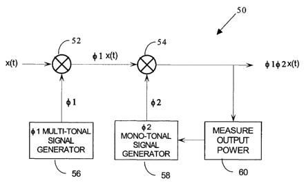
A circuit which addresses a number of the objects outlined above is
presented as a block diagram in Figure 2. This figure presents a demodulator
topology 50 in which an input signal x(t) is down-converted by mixing it with
two
mixing signals cps and cps. As will be described, these two mixing signals are
cp, and
cps are very different from mixing signals used in normal two-step conversion
topologies (such as superheterodyne topologies). The main difference from the
direct-conversion approach is that two mixing signals of the invention are
used to
emulate the single mixing signal, and they do this without the usual
shortcomings of
direct-conversion, such as self-mixing.
As shown in Figure 2, the input signal x(t) is mixed with a multi-tonal mixing
signal cp, using a first mixer 52 (multi-tonal, or non-mono-tonal, refers to a
signal
having more than one fundamental frequency tone. Mono-tonal signals have one
fundamental frequency tone and may have other tones that are harmonically
related
to the fundamental tone). The resulting signal, cp1 x(t), is then mixed with a
mono-
tonal signal cp2 by means of a second mixer 54, generating an output signal
cp1 cp2
x(t). These mixing signals cp1 and cp2 are generally referred to herein as
"virtual local
oscillator" (VLO) signals as they emulate a local oscillator signal; the
product cp1 * cp2
having significant power at the frequency of a local oscillator signal being
emulated.
In the preferred embodiment, neither cp1 nor cp2 have significant power at the
frequency of the input signal x(t), the LO signal being emulated, or the
output signal
cp1 cp2 x(t), but these restrictions can be somewhat relaxed. Mixing signals
with such
characteristics greatly resolve the problem of self-mixing because the VLO
signals
simply do not have significant power at frequencies that will appear in the
output
signal.
These VLO signals are described in greater detail hereinafter, but an
exemplary pair of cp1 and cp2 mixing signals is presented in Figure 3, plotted
in
amplitude versus time. It is important to note from Figure 3 that:
1. ep1 is not mono-tonal (it is multi-tonal);
2. cp2 is mono-tonal;
3. that the product of cp1 and cp2; that is cp1 * cp2, is clearly equivalent
to the LO
signal being emulated. Thus, the output of this demodulation topology, cp1
CA 02477310 2004-08-24
WO 03/071673 PCT/CA03/00257
-7-
cp2 x(t), will be equal to the output of a hypothetical LO * x(t) down
converter;
and
4. that neither of cp1 nor cp2 have significant power at the frequency of the
LO
signal being emulated.
It is also important to note that at no point in the operation of the circuit
is an actual
"cp1 * cp2" signal ever generated and if it is, only an insignificant amount
is generated.
The mixers 52, 54 receive separate cp1 and cp2 signals, and mix them with the
input
signal x(t) using different physical components. Hence, there is no LO signal
which
may leak into the circuit.
Looking at one cycle of these mixing signals from Figure 3 the generation of
the cp1 * cp2 signal is clear:
cp 1 cp2 cp 1 *
cp2
LO LO LO
HI LO HI
LO LO LO
HI LO HI
HI HI LO
LO HI HI
HI HI LO
LO HI HI
These mixing signals can be generated in many ways, a number of which are
described in co-pending patent applications (see for example, co-pending
patent
applications filed under PCT International Application Serial Nos.
PCT/CA00/00994,
PCT/CA00/00995 and PCT/CA00/00996). The multi-tonal signal generator 56, fo'r
example, can consist of an oscillator operating at a fixed frequency and a
linear
feedback shift register (LFSR) circuit. Such LFSR circuits are often used to
generate similar sequences in CDMA (code division multiple access)
communication
systems. The mono-tonal signal generator 58, of course, could consist simply
of an
oscillator.
While the use of VLO mixing signals is very effective, there will be power
generated in places other than the RF carrier frequency; "unwanted power"
which
can be seen in the frequency spectrum test data of Figure 4. This amount of
unwanted power can be controlled via the time delay and frequency of signal
cp2.
CA 02477310 2004-08-24
WO 03/071673 PCT/CA03/00257
-g-
The unwanted power will down convert signals located at the "unwanted power
frequencies". For example, if there is unwanted power at 2100MHz and there is
an
out of band RF signal at 2100MHz, this RF signal will be down converted on top
of
the wanted signal. However, this down converted power will be attenuated by
the
difference between "the power of the wanted" minus "the power of the unwanted"
(for Figure 4 this is ~37dB). We refer to this difference herein as WmU
(Wanted
minus Unwanted).
If RFwanted denotes the wanted RF power, the total amount of power at
baseband is approximately:
BBpower = RFwanted + 10"(-WmU/10)*RFunwanted (1 )
There are two straightforward ways to fix this problem:
1. adjusting the time delay of cp2, thereby modifying the value of WmU; or
2. adjusting the frequency of cp2 such that the RFunwanted tone does not fall
on
top of the wanted signal at baseband.
In either approach the BBpower is minimized as a function of the variables in
1 or 2.
The document addresses solution 2, but can equally apply to 1, by renaming
variables.
Accordingly, the topology of Figure 2 is provided with a power measurement
circuit 60 for measuring the power of said output signal cp1 cp2 x(t) at the
baseband
frequency. This power measurement circuit 60 feeds back to the mono-tonal
signal
generator 58 and is used to manipulate the parameters of the cp2 mixing signal
to
minimize the power of the output signal cp1 cp2 x(t). In general, any
parameter of cp2
could be manipulated depending on the design parameters of the circuit and the
nature of the noise that is to be suppressed. In the preferred embodiment
described
hereinafter, the focus is on manipulating the frequency of the cp2 signal, but
phase,
amplitude or wave shape could also be manipulated.
The nature of the parameter of the cp2 signal being manipulated will also
dictate the design of the mono-tonal signal generator 58. If the frequency of
the cp2
signal is being manipulated, the mono-tonal signal generator 58 can simply
consist
of a voltage controller oscillator (VCO) in conjunction with a phase-locked
loop (PLL).
While this circuit contains many components that are similar to commonly
used demodulation topologies, it uses them in a unique way. Thus, this
circuit:
1. allows an input signal x(t) to be down-converted using a completely
integratable circuit;
2. does not use mixing signals that contain significant power at the frequency
of
CA 02477310 2004-08-24
WO 03/071673 PCT/CA03/00257
_g_
the local oscillator signal being emulated. Thus, the frequency translation is
still effected, but self-mixing and unwanted mixing products are avoided; and
3. is particularly convenient when applied to the development of multi-
standard/multi-frequency devices because no filters are required, and
because a wide variety of mixing signals can easily be generated and
manipulated. A digital signal processor (DSP) for example, could be used to
coordinate mixing signals for a large number of standards and frequencies in
a single device.
Other advantages of the invention will also become clear from the other
embodiments of the invention described hereinafter.
Note that particular design parameters for the two mixers 52 and 56 would be
clear to one skilled in the art, having the typical properties of an
associated noise
figure, linearity response, and conversion gain. The selection and design of
these
mixers would follow the standards known in the art.
The power measurement device 60 may also one of many known in the art.
Power measurement is often provided as an extra output, for example, in RF
amplifiers as an RSSI (received-signal strength indicator) output.
Though Figure 2 implies that various elements are implemented in analogue
form, they can also be implemented in digital form. The mixing signals are
typically
presented herein in terms of binary 1s and Os, however, bipolarwaveforms, ~1,
may
also be used. Bipolar waveforms are typically used in spread spectrum
applications
because they use commutating mixers which periodically invert their inputs in
step
with a local control signal (this inverting process is distinct from mixing a
signal with a
local oscillator directly).
A number of other embodiments of the invention will now be described.
Description of Preferred Embodiments of the Invention
The preferred embodiment of the invention is presented as a block diagram
in Figure 5. At the core, this topology consists of two mixers 72, 74
connected
together via a high pass filter (HPF) 76. At the LO ports of the two mixers
72, 74
VLO mixing signals cp1 and cp2 are applied such that the incoming RF signal,
x(t), is
multiplied by a signal having significant power at the RF carrier frequency of
x(t),
downconverting it to baseband.
The first mixer 72 is preferably an active mixer, and the second mixer 74, a
passive mixer. Active mixers are distinct from passive mixers in a number of
ways:
CA 02477310 2004-08-24
WO 03/071673 PCT/CA03/00257
-10-
1. they provide conversion gain; thus, an active mixer can replace the
combination of a low noise amplifier and a passive mixer;
2. active mixers provide better isolation between the input and output ports
because of the impedance of the active components; and
3. active mixers allow a lower powered mixing signal to be used, reducing the
noise that results when the mixing signal is generated.
In spite of these advantages, the application of active mixers in modulation
and demodulation topologies is still problematic. Because active mixers are
non-
linear devices, they generate more "1/f' noise and produce second-order
distortion.
This noise is called 1/f noise because its power spectra is generally
inversely
proportional to the frequency - in other words, the power of the noise signal
is
greater, close to DC (direct current).
In the topology of the invention, this second-order distortion is removed
using
the high pass filter (HPF) 76. Because the second mixer 74 is a passive mixer
and it
operates at a relatively lower mixing frequency, it introduces significantly
less
second-order distortion into the signal. Thus, this topology provides the
benefits of
active mixing, without introducing second-order distortion into the output
signal.
As noted above, the multi-tonal signal generator 56 can be implemented in a
manner known in the art. In general, the multi-tonal signal generator 56 will
be fed
with an oscillator signal of some sort, as known in the art. Note that if the
invention
is applied in a multi-band application, for which it is well suited, it may be
necessary
for the multi-tonal signal generator 56 and oscillator 78 to have a broad
range of
operation.
The components that generate the cp2 mixing signal are presented as a
block diagram in Figure 5, but are described in greater detail with respect to
Figures
6 - 10. At the heart of the cp2 generation circuit lies the frequency control
circuit 80.
Its role is to receive data on the output power from mixer 74 and the power
measuring device 60, and to use this data to manipulate the frequency of
mixing
signal cp2 to minimize this output power. In the preferred embodiment, mixing
signal
cp2 is generated using a voltage controlled oscillator (VCO) 82, so the
frequency
control circuit 80 is simply designed to adjust the output of the VCO 82
within the
desired frequency range for cp2. By minimizing the power at baseband as a
function
of cp2, this solution pushes the unwanted power to a location in which it does
not
cause problems.
In the preferred embodiment, the power measuring device 60 provides a
CA 02477310 2004-08-24
WO 03/071673 PCT/CA03/00257
-11 -
digital-byte output, but of course, it could also be provided in other forms.
The
frequency controller 80 receives these digital power measurement signals and
determines whether the output power level is rising or falling. It does this
simply by
comparing the current power level with an earlier, stored power level. If the
power
level has fallen since this earlier, stored power level was received, then it
is clear that
any incremental frequency adjustments the frequency controller 80 has been
directing the VCO 82 to make, are progressing toward a minimum power level.
The
frequency controller 80 should therefore advise the VCO 82 to continue
adjusting the
frequency of cp2 in the same manner.
If the power level has risen since the earlier, stored power level was
received,
then clearly the frequency controller 80 and VCO 82 are making adjustments
away
from the minimum power level, so the sense of the adjustments should be
inverted
(i.e. if positive increments in the frequency of cp2 were being made when a
rise in
power was detected, then these should be switched to negative frequency
adjustments. Conversely, if negative adjustments were being made when a rise
in
power was detected, then these should be switched to positive frequency
adjustments). Any circuit which performs a similar kind of power analysis and
cp2
frequency adjustment could be used.
In the preferred embodiment described hereinafter, an external clock 84 is
used to supervise the sampling of power measurements, and set the time
differential
between the stored power measurement and the current power measurement. This
signal could also be provided by a micro-controller, digital signal processor
or similar
processing device, and does not have to be uniformly periodic.
Also in the preferred embodiment, delay latches and feedback loops are used
in the frequency controller 80. It is therefore necessary to set the initial
conditions
for the frequency controller 80 using some manner of control circuit 86. Like
the
external clock 84, the functionality of this initial condition control circuit
86 could be
provided by a micro-controller, digital signal processor or similar processing
device,
or could simply be provided using gate logic or an ASIC (application specific
integrated circuit).
The frequency control circuit 80 may also take many forms. In a simple
implementation, it may consist of several simple logic and linear components.
Alternatively, it may be implemented almost completely in software on a DSP.
More
complex implementations such as multi-standard devices will typically
incorporate a
lot of the frequency control circuit's functionality on DSPs or ASICs.
CA 02477310 2004-08-24
WO 03/071673 PCT/CA03/00257
-12-
The voltage controlled oscillator (VCO) 94, is a standard VCO as known in
the art, generating mono-tonal signals in the range dictated by the operating
range
of the demodulator 70. As well, the control voltage input will have to be
compatible
with the output of the frequency control circuit 80, but that is a
straightforward design
matter. In the preferred embodiment described hereinafter the analogue control
input to the VCO 82 has a range of 800mV to 1.15V, which results in a
frequency
variation of ~160MHz to -40MHz on the cp2 output, but these values are
completely
design dependent.
An exemplary embodiment of the frequency control circuit 80 will now be
described with respect to Figures 6 - 10.
An exemplary circuit for the frequency control circuit 80 is presented in the
block diagram of Figure 6. Note that the P;, P;_,, a ; and a ;_, signals are
digital byte
data, while the outputs of the two Sgn functions are either +1 or -1 values.
This
circuit operates as follows:
1. the initial power at the it" step, P;, is received and is passed through a
delay
latch 90, so that an historic power measurement P;_, (the power at the i-1
step) can be stored;
2. the difference between the current and stored power measurements P; and
P;_, is then calculated using adder 92;
3. the sign of this difference (either +1 or -1 ) is then determined using the
Sgn(P;- P;_,) function 94;
4. the output of this. Sgn(P;- P;_,) function 94 is then multiplied with the
sign of
the difference of the a values, Sgn(a ; - a ;_,) using the multiplier 96;
5. the output of the multiplier 96 is fed to an inventor 98 (at this point the
signal
is referred to herein as "x"), and then to an optional loop filter 100. The
loop
filter 100 may be necessary to provided additional stability. Note that x is a
bit value which establishes whether a; is to be increased or decreased (this
inventor 98 can be removed in some cases);
6. the filtered x signal is then input to an adder 102, where it is added to a
;.
The initial value of a ; is a digital byte or word which corresponds to the
desired initial value of the output SO SEL RX. The initial a value sets the
initial frequency output of the VCO 82;
7. the output of the adder 102, is then delayed by delay latch 104, which
becomes the next a ;;
CA 02477310 2004-08-24
WO 03/071673 PCT/CA03/00257
-13-
8. the a ; signal is then delayed again using delay latch 106, to store an
historic
a ;_, value;
9. the difference between a ; and a ;_, is then calculated using adder 108,
and
the sign of this difference is taken using the Sgn(a ; - a ;_,) function 110.
This
generates the Sgn(a ; - a ;_,) signal which is fed back into the multiplier
96;
and
10. as suggested above, a ; sets the frequency of the VCO 82, so it will
generally
be converted to an analogue form using the digital to analogue convertor
112, and be fed to the VCO 82. This output signal is labelled SO SEl-_RX in
Figure 6.
As noted above, it will generally be necessary to initialize the values of the
signals in the frequency control circuit 80. Typically, a register of some
sort can be
used to load in appropriate values for the P;, P;_,, a ; and a ;_, signals. It
is possible
that the Sgn functions will return zero values if the differences are less
than some
selected value.
An exemplary operating cycle of this circuit might proceed as follows:
i. P. P. a. a. S n P.-P.S n a.-a. x
initial0 max 0 max -1 -1 -1
1 5 0 -1 0 1 -1 1
2 4 5 0 -1 -1 1 1
3 3 4 1 0 -1 1 1
4 2 3 2 1 -1 1 1
5 1 2 3 2 -1 1 1
6 0 1 4 3 -1 1 1
7 1 0 5 4 1 1 -1
8 0 1 4 5 -1 -1 -1
9 1 0 3 4 1 -1 1
10 0 1 4 3 -1 1 ~ 1
Note that the x value determines whether the a signal will be incremented or
decremented on the next loop. Also note that this loop results in the output
to the
VCO 82 being incremented one step at a time. This results in a step up or down
of
5.5mV to the VCO 82. This control circuit can easily be altered to result in
larger or
smaller steps.
Figure 7 presents a graph of the relationship between the output power P
and control signal a, per the exemplary table above. At startup, the output
power P
is at a level of 5, and a is at -1. The power level P drops as a rises, power
level P
CA 02477310 2004-08-24
WO 03/071673 PCT/CA03/00257
-14-
being minimized at 0, which corresponds to an a value of 4. The power level P
then
vacillates between 0 and 1, as a hunts between 3 and 5.
Figures 8 and 9 present block diagrams of how the circuit of Figures 5 and 6
might be applied.
When starting up, it would be desirable to set the frequency of cp2 at an
ideal
theoretical level. The circuit 120 of Figure 5 is used to accomplish this,
incorporating an automatic gain control (AGC) loop 122 to set the input to the
VCO
82. As shown in Figure 5, the frequency control circuit 80 and the AGC control
loop
122 are connected in parallel, and both receive the power level input P;.
However,
the output of only one of these two devices will be fed to the VCQ 82, which
is
controlled by the enableldisable input 124. This enable/disable input 124 can
be
controlled using a threshold detector, or could be provided by a.DSP or
similar
processing device.
The operation of this circuit 120 preferable proceeds as follows:
1. the AGC control loop 122 is first initialized to find the correct gain;
then
2. the AGC control loop 122 is disabled and the frequency control circuit 80
is
turned on;
3. if the power at the input to the frequency control circuit 80 goes below
some
critical value the frequency control circuit 80 is disabled and the AGC
control
loop 122 is enabled;
4. once a reasonable power level P; is detected at the input, the frequency
control circuit 80 is again enable and the AGC control loop 122 is disabled.
This process will continue until the frequency control circuit 80 becomes
stable.
During operation mode of the circuit, the frequency control circuit 80 can be
adjusted, but it is important that the AGC control loop 122 be disabled during
this
adjustment.
Also note that while the frequency control circuit 80 is deactivated, the
values
of a ; and a ;_, should be fixed, while the power values P; and P;_, should be
continuously updated. The components affected by this are shown in Figure 9,
the
components being updated being enclosed in block 130, and the components which
should hold there values being enclosed in block 132.
Software Implementation
The invention can be implemented in many forms, incorporating hardware,
CA 02477310 2004-08-24
WO 03/071673 PCT/CA03/00257
-15-
software, or a combination of the two. The invention could, for example, be
implemented in an existing digital signal processor (DSP) with almost no
hardware
modifications.
An exemplary methodology is presented in Figure 10. This methodology is
implemented by performing the following steps:
1. generating a multi-tonal mixing signal cp1 at step 140;
2. generating a mono-tonal mixing signal cp2 at step 142, where cp1 * cp2 has
significant power at the frequency of the local oscillator signal being
emulated, and neither of the cp1 nor the cp2 having significant power at the
frequency of an input signal x(t), the LO signal being emulated, or an output
signal cp1 cp2 x(t);
3. at step 144, mixing the input signal x(t) with the multi-tonal mixing
signal cp1,
to generate an output signal cp1 x(t);
4. at step 146, mixing the signal cp1 x(t) with the mono-tonal mixing signal
cp2, to
generate an output signal cp1 cp2 x(t);
5, measuring the power of the output signal cp1 cp2 x(t) at step 148; and
6. adjusting the characteristics of the mono-tonal mixing signal cp2 at step
150 to
minimize the power of the output signal cp1 cp2 x(t), and returning to step
142.
Modifications to this methodology would be clear from a reading of the balance
of
this document.
Virtual Local Oscillator Signals
An exemplary set of VLO signals were described hereinabove. The purpose
of this section is to present VLO signals in a more general way, as any number
of
VLO signals could be generated with which the invention could be implemented.
Aperiodic or time-varying mixing signals offer advantages over previously
used mono-tonal oscillator signals. A given pair of these virtual local
oscillator (VLO)
signals cp1 and cp2 have the properties that:
1. their product emulates a local oscillator (LO) signal that has significant
power
at the frequency necessary to translate the input signal x(t) to the desired
output frequency. For example, to translate the input signal x(t) to baseband,
cp1 (t) * cp2(t) must have a frequency component at the carrier frequency of
x(t); and
2. one of either cp1 and cp2, has minimal power around the frequency of the
mixer pair output cp1 (t) * cp2(t) * x(t), while the other has minimal power
CA 02477310 2004-08-24
WO 03/071673 PCT/CA03/00257
-16-
around the centre frequency, fRF, of the input signal x(t). "Minimal power"
means that the power should be low enough that it does not seriously
degrade the performance of the RF chain in the context of the particular
application.
For example, if the mixer pair is demodulating the input signal x(t) to
baseband, it is preferable that one of either cp1 and cp2 has minimal power
around DC.
As a result, the desired demodulation is affected, but there is no LO signal
to leak
into the signal path and appear at the output.
As noted above, mixing two signals together generates an output with:
(a) a signal equal in frequency to the sum of the frequencies of the input
signals;
(b) a signal equal in frequency to the difference between the frequencies of
the
input signals; and
(c) the original input frequencies.
Thus, direct conversion receivers known in the art must mix the input signal
x(t) with
a LO signal at the carrier frequency of the input signal x(t). If the LO
signal of a
direct conversion receiver leaks into the signal path, it will also be
demodulated to
baseband along with the input signal x(t), causing interference. The invention
does
not use an LO signal, so leakage does not generate a signal at the baseband
output
cp1 (t) * cp2(t) * x(t).
Any signal component at the frequency of the input signal x(t) or output cp1
(t)
* cp2(t) * x(t), in either of the mixing signals cp1 and cp2, is suppressed or
eliminated
by the other mixing signal. For example, if the mixing signal cp2 has some
amount of
power within the bandwidth of the up-converted RF (output) signal, and it
leaks into
the signal path, then it will be suppressed by the cp1 mixing signal which has
minimal
power within the bandwidth of the up-converted RF (output) signal. This
complementary mixing suppresses interference from the mixing signals cp1 and
cp2.
As noted above, current receiver and transmitter technologies have several
problems. Direct-conversion transceivers, for example, suffer from LO leakage
and
1/f noise problems which limit their capabilities, while heterodyne
transceivers
require image-rejection techniques which are difficult to implement on-chip
with high
levels of performance.
The problems of image-rejection, LO leakage and 1/f noise in highly
integrated transceivers can be overcome by using the complementary VLO
signals.
These signals are complementary in that one of the cp1 and cp2 signals has
minimal
CA 02477310 2004-08-24
WO 03/071673 PCT/CA03/00257
_ _ __ __
-17-
power around the frequency of the output signal y(t) (which is around DC if
conversion is to baseband), and the other has minimal power around the centre
frequency, fRF, of the input signal x(t).
These signals cp1 and cp2 can, in general, be:
1. random or pseudo-random, periodic functions of time;
2. analogue or digital waveforms;
3. constructed using conventional or non-conventional bipolar waves;
4. averaging to zero;
5. amplitude modulated; and
6, generated in a number of manners including:
a. being stored in memory and clocked out;
b. being generated using digital blocks;
c. being generated using noise shaping elements (e.g. delta-sigma
elements); or
d. being constructed using PN sequences with additional bits inserted so
they comply to the above conditions.
It would be clear to one skilled in the art that virtual LO signals may be
generated which provide the benefits of the invention to greater or lesser
degrees.
While it is possible in certain circumstances to have almost no LO leakage, it
may be
acceptable in other circumstances to incorporate virtual LO signals which
still allow a
degree of LO leakage.
Virtual local oscillator signals may also be generated in different forms,
such
as using three or more complementary signals rather than the two mixing
signals
shown above. These and other variations are described in the following co-
pending
patent applications:
1. PCT International Application Serial No. PCT/CA00/00995 Filed September
1, 2000, titled: "Improved Method And Apparatus For Up-Conversion Of
Radio Frequency (RF) Signals";
2. PCT International Application Serial No. PCT/CA00/00994 Filed September
1, 2000, titled: "Improved Method And Apparatus For Down-Conversion Of
Radio Frequency (RF) Signals"; and
3. PCT International Application Serial No. I'CT/CA00/00996 Filed September
1, 2000, titled: "Improved Method And Apparatus For
Up-And-Down-Conversion Of Radio Frequency (RF) Signals".
CA 02477310 2004-08-24
WO 03/071673 PCT/CA03/00257
-18-
In-Phase and Quadrature Signals
In many modulation schemes, it is necessary to modulate or demodulate both
in-phase (I) and quadrature (Q) components of the input signal.
In such a case, four modulation functions would have to be generated: cp1 I
which is 90 degrees out of phase with cp1Q; and cp21 which is 90 degrees out
of
phase with cp2Q. The pairing of signals cp1 I and cp21 must meet the function
selection
criteria listed above, as must the signal pairing of cp1Q and cp2Q.
Design of components to generate and manipulate such signals would be
clear to one skilled in the art from the description herein. As well,
additional details
on the generation of such signals are available in the co-pending patent
applications
filed under PCT International Application Serial Nos. PCT/CA00/00994,
PCT/CA00100995 and PCT/CA00/00996.
Advantages of the Invention
The invention provides many advantages over down convertors known in the
art. As noted above, the invention allows spurs to be reduced and moved away
from
the signal of interest, by minimizing the baseband power with respect to the
location
of the unwanted power.
The invention also offers the following:
1. minimal 1/f noise;
2. minimal imaging problems;
3. minimal leakage of a local oscillator (LO) signal into the RF output band;
4. has a higher level of integration as the components it does require are
easily
placed on an integrated circuit., For example, no large capacitors or
sophisticated filters are required; and
5. it is well suited to multi-band, multi-standard applications because of the
integrated nature of the design. The circuits of the invention can operate
effectively with a very wide range of mixing signals cp1 and cp2, and these
mixing signals can easily be generated by suitable control components.
A high level of integration results in decreased IC (integrated circuit) pin
counts, decreased signal power loss, decreased IC power requirements, improved
SNR (signal to noise ratio), improved NF (noise factor), and decreased
manufacturing costs and complexity. The design of the invention therefore
makes
the production of inexpensive multi-standard/multi-frequency communications
transmitters and receivers a reality.
CA 02477310 2004-08-24
WO 03/071673 PCT/CA03/00257
-19-
The benefits of the invention are most apparent when it is implemented within
a single-chip design, eliminating the extra cost of interconnecting
semiconductor
integrated circuit devices, reducing the physical space they require and
reducing the
overall power consumption. Increasing levels of integration have been the
driving
impetus towards lower cost, higher volume, higher reliability and lower power
consumer electronics since the inception of the integrated circuit. This
invention will
s
enable communications devices to follow the same integration route that other
consumer electronic products have benefited from.
Options and Alternatives
A number of variations can be made to the topologies described herein,
including the following:
1. the circuits of the invention were described in digital domain. They can
also
be expressed in analog domain;
2. the Sgn functions 94, 110 can be removed if an appropriate multiplier 96 is
used which ignores the irrelevant bits;
3. differential signaling could be used for some or all of the components in
this
design. Differential signals are signals having positive and negative
potentials with respect to ground, rather than a single potential with respect
to
ground. The use of a differential architecture results in stronger output
signals that are more immune to common mode noise.
The generation of differential VLO signals is straightforward because a given
pair of differential VLO signals are simply complements of one another.
Adapting cp1 to a differential architecture simply requires the generation of
a
complementary cp1 P and cp1 N pair, where cp1 P and cp1 N are inverses of one
another, that is: cp1 P = - (cp1 N);
4. various mixer designs could be used as known in the art, such as:
a. single or double-balanced mixers. Single-balanced mixers will
generate less noise than double-balanced mixers simply because
there are fewer noise contributors in the single-balanced design.
However, single-balanced mixers are less immune to external noise,
particularly common mode noise;
b. active or passive mixers;
c. active mixers with adjustable performance. A suitable active mixer is
described in the co-pending patent application filed under Canadian
CA 02477310 2004-08-24
WO 03/071673 PCT/CA03/00257
-20-
Patent Application Serial No. 2,375,438, titled: "Improvements to a
High Linearity Gilbert I Q Dual Mixer". This mixer has adjustable gain
and adjustable current source. Gain-control is provided by means of
a number of different input transistors, each being fed with the same
input signal. The amount of biasing current is controlled by using a
number of current sources which are electronically switched in and
out of the circuit as required; and
5. a high pass filter 76 which incorporates a voltage divider, could be used
to
set the common mode output.
Conclusions
It will be apparent to those skilled in the art that the invention can be
extended to cope with more than two or three standards, and to allow for more
biasing conditions than those in the above description.
The electrical circuits of the invention may be described by computer
software code in a simulation language, or hardware development language used
to
fabricate integrated circuits. This computer software code may be stored in a
variety
of formats on various electronic memory media including computer diskettes, CD-
ROM, Random Access Memory (RAM) and Read Only Memory (ROM). As well,
electronic signals representing such computer software code may also be
transmitted via a communication network.
Clearly, such computer software code may also be integrated with the code
of other programs, implemented as a core or subroutine by external program
calls,
or by other techniques known in the art.
The embodiments of the invention may be implemented on various families of
integrated circuit technologies using digital signal processors (DSPs),
microcontrollers, microprocessors, field programmable gate arrays (FPGAs), or
discrete components. Such implementations would be clear to one skilled in the
art.
The various preferred implementations in this section are each described in
terms of field effect transistors. The implementations are equally
advantageous
when other technologies are used, including, but not limited to CMOS or
Bipolar
Junction Transistors. Similarly, suitable fabrication technologies other than
Silicon
(Si) may be used, including, but not limited to SiliconlGermanium (SiGe),
Germanium (Ge), Gallium Arsenide (GaAs), and Silicon on Sapphire (SOS). It is
the
inventors' intention to protect all such implementations.
CA 02477310 2004-08-24
WO 03/071673 PCT/CA03/00257
-21 -
The invention may be applied to various communication protocols and
formats including: amplitude modulation (AM), frequency modulation (FM),
frequency
shift keying (FSK), phase shift keying (PSK), cellular telephone systems
including
analogue and digital systems such as code division multiple access (CDMA),
time
division multiple access (TDMA) and frequency division multiple access (FDMA).
The invention may be applied to such applications as wired communication
systems include computer communication systems such as local area networks
(LANs), point to point signalling, and wide area networks (WANs) such as the
Internet, using electrical or optical fibre cable systems. As well, wireless
communication systems may include those for public broadcasting such as AM and
FM radio, and UHF and VHF television; or those for private communication such
as
cellular telephones, personal paging devices, wireless local loops, monitoring
of
homes by utility companies, cordless telephones including the digital cordless
European telecommunication (DECT) standard, mobile radio systems, GSM and
AMPS cellular telephones, microwave backbone networks, interconnected
appliances under the Bluetooth standard, and satellite communications.
While particular embodiments of the present invention have been shown and
described, it is clear that changes and modifications may be made to such
embodiments without departing from the true scope and spirit of the invention.