Note: Descriptions are shown in the official language in which they were submitted.
CA 02477650 2004-08-16
03-1-549
BALLAST WITH LOAD-ADAPTABLE FAULT DETECTION CIRCUIT
Field of the Invention
The present invention relates to the general subject of circuits for
powering discharge lamps. More particularly, the present invention relates to
a
ballast with a fault detection circuit that adapts to the lamp load.
Background of the Invention
Many electronic ballasts for powering gas discharge lamps include a
driven half-bridge inverter and a series resonant output circuit. Such
ballasts
generally include some form of protection circuitry for preventing damage to
the
inverter and other portions of the ballast in the event of a lamp fault
condition.
Common lamp fault conditions include lamp removal or lamp failure.
A popular protection approach is to place a current-sensing resistor in
series with the lower inverter transistor, monitor the voltage across the
current-
sensing resistor, and shut down the inverter if the voltage across the current-
sensing resistor exceeds a predetermined threshold value. While this approach
is
adequate for protecting against certain fault conditions, such as lamp removal
or
lamp failure, it does not adequately protect against less well-defined fault
conditions, such as the arcing that occurs when a slight air gap is introduced
between the pins of a lamp and the sockets of the lighting fixture. Under such
an
emergent arcing situation, the voltage that develops across the current-
sensing
resistor will not necessarily be high enough to exceed the predetermined
threshold value, in which case the inverter will continue to operate and the
potentially dangerous arcing condition will be allowed to continue unabated.
Simply lowering the resistance of the current-sensing resistor (and, thus,
the predetermined threshold value) is not a successful remedy to this problem,
because that might result in the inverter being improperly shut down even in
the
absence of a legitimate fault condition. This is especially true for ballasts
that
must be capable of powering several different types of lamps (e.g., F17T8,
F25T8, and F32T8 lamps), in which case the current that flows through the
current-sensing resistor during normal operation (i.e., with no fault
condition
CA 02477650 2011-06-09
2
present) may vary over a considerable range. Thus, in order to avoid false
detection of a
fault, the predetermined threshold value must be set such that the current
though the
current-sensing resistor must be much higher than the normal operating value
before a
fault is detected. Of course, when a mild arcing condition occurs, the current
that flows
through the current-sensing resistor may increase only modestly above its
normal
operating value, in which case the predetermined fault threshold will not be
reached and
the inverter be allowed to continue to operate.
What is needed, therefore, is a ballast with a fault detection circuit that is
capable
of quickly and accurately responding to an arcing condition in the lamp load.
Such a
ballast would represent a significant advance over the prior art.
Summary of the Invention
In accordance with an aspect of the present invention, there is provided a
ballast,
comprising: an inverter, comprising: first and second input terminals adapted
to receive a
source of direct current (DC) voltage; an inverter output terminal; an output
circuit
coupled to the inverter output terminal, the output circuit comprising first
and second
output connections for coupling to a lamp load comprising at least one gas
discharge
lamp; a fault detection circuit coupled between the output circuit and the
inverter,
wherein the fault detection circuit is operable: (i) to monitor a first signal
and a second
signal within the output circuit; (ii) to set a fault threshold in dependence
on the second
signal; and (iii) in response to the first signal exceeding the fault
threshold, to issue a
shutdown command directing the inverter to cease operation. The fault
detection circuit
comprises: first and second inputs coupled to the output circuit; an output
coupled to the
inverter; a first diode having an anode coupled to circuit ground and a
cathode coupled to
the second input; a second diode having an anode coupled to the second input
and a
cathode coupled to a first node; a first resistor coupled between the first
node and a
second node; a second resistor coupled between the second node and circuit
ground; a
first transistor having a gate, a drain, and a source, the source being
coupled to circuit
ground; a third resistor coupled between the second node and the gate of the
first
transistor; a second transistor having a gate, a drain, and a source, the
source being
coupled to circuit ground; a fourth resistor coupled between the first node
and the gate of
CA 02477650 2011-06-09
2a
the second transistor; a fifth resistor coupled between the first input and a
third node; a
sixth resistor coupled between the third node and the drain of the first
transistor; a
seventh resistor coupled between the drain of the first transistor and the
drain of the
35 second transistor; an eighth resistor coupled between the drain of the
second transistor
and circuit ground; a third transistor having a gate, a drain, and a source,
the gate being
coupled to the third node and the source being coupled to circuit ground; a
ninth resistor
coupled between a direct current (DC) voltage supply and the drain of the
third transistor,
a fourth transistor having a base, an emitter, and a collector, the base being
coupled to the
40 drain of the third transistor and the collector being coupled to the DC
voltage supply; a
tenth resistor coupled between the emitter of the fourth transistor and
circuit ground; and
a third diode having an anode coupled to the emitter of the fourth transistor
and a cathode
coupled to the output.
In accordance with another aspect of the present invention, there is provided
a
45 ballast, comprising: an inverter, comprising: first and second input
terminals adapted to
receive a source of direct current (DC) voltage; an inverter output terminal;
upper and
lower inverter transistors; and an inverter driver circuit coupled to the
upper and lower
inverter transistors and operable to commutate the inverter transistors in a
complementary
manner, the inverter driver circuit having a shutdown input wherein the
inverter driver
50 circuit is operable, in response to receipt of a shutdown command at the
shutdown input,
to cease commutating the inverter transistors; a fault detection circuit,
comprising: first
and second inputs; an output coupled to the shutdown input of the inverter
driver circuit;
an output circuit, comprising: first and second output connections for
coupling to a lamp
load comprising at least one gas discharge lamp; a resonant inductor coupled
between the
55 inverter output terminal and the first output connection, the first
output connection being
coupled to the first input of the fault detection circuit; and a resonant
capacitor coupled
between the first output connection and the second input of the fault
detection circuit, the
resonant capacitor having a resonant capacitor voltage and a resonant
capacitor current;
and wherein the fault detection circuit is operable: (i) to monitor the
resonant capacitor
60 voltage and the resonant capacitor current; (ii) to set a fault
threshold in dependence on
the resonant capacitor current; and (iii) in response to the resonant
capacitor voltage
exceeding the fault threshold, to send the shutdown command to the inverter
driver
CA 02477650 2011-06-09
2b
circuit. The fault detection circuit further comprises: a first diode having
an anode
coupled to circuit ground and a cathode coupled to the second input; a second
diode
65 having an anode coupled to the second input and a cathode coupled to a
first node; a first
resistor coupled between the first node and a second node; a second resistor
coupled
between the second node and circuit ground; a first transistor having a gate,
a drain, and a
source, the source being coupled to circuit ground; a third resistor coupled
between the
second node and the gate of the first transistor; a second transistor having a
gate, a drain,
70 and a source, the source being coupled to circuit ground; a fourth
resistor coupled
between the first node and the gate of the second transistor; a fifth resistor
coupled
between the first input and a third node; a sixth resistor coupled between the
third node
and the drain of the first transistor; a seventh resistor coupled between the
drain of the
first transistor and the drain of the second transistor; an eighth resistor
coupled between
75 the drain of the second transistor and circuit ground; a third
transistor having a gate, a
drain, and a source, the gate being coupled to the third node and the source
being coupled
to circuit ground; a ninth resistor coupled between a direct current (DC)
voltage supply
and the drain of the third transistor; a fourth transistor having a base, an
emitter, and a
collector, the base being coupled to the drain of the third transistor and the
collector being
80 coupled to the DC voltage supply; a tenth resistor coupled between the
emitter of the
fourth transistor and circuit ground; and a third diode having an anode
coupled to the
emitter of the fourth transistor and a cathode coupled to the output.
Brief Description of the Drawings
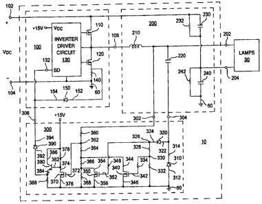
Figure 1 is a partial block-diagram schematic of a ballast with a fault
detection
85 circuit, in accordance with a preferred embodiment of the present
invention.
Figure 2 is a detailed schematic of a ballast with a fault detection circuit,
in
accordance with a preferred embodiment of the present invention.
Detailed Description of the Preferred Embodiments
90 In a preferred embodiment of the present invention, as described in
Figure 1, a
ballast 10 includes an inverter 100, an output circuit 200, and a fault
detection circuit 300.
Inverter 100 comprises first and second input terminals 102,104 and an
inverter
output terminal 106. Input terminals 102,104 receive a source of substantially
direct
CA 02477650 2011-06-09
2c
current (DC) voltage, VDC VDc may be provided by any of a number of
arrangements
95 known to those skilled in the art; one such arrangement
CA 02477650 2004-08-16
3
consists essentially of a full-wave rectifier (coupled to a source of
conventional
60 hertz alternating current) followed by a boost converter.
Output circuit 200 is coupled to inverter output terminal 106 and
includes first and second output connections 202,204 for coupling to a lamp
load 30 comprising at least one gas discharge lamp.
Fault detection circuit 300 is coupled between output circuit 200 and
inverter 100. During operation, fault detection circuit 300 monitors a first
signal
and a second signal within output circuit 200, and sets a fault threshold in
dependence on the second signal. In response to the first signal exceeding the
fault threshold, fault detection circuit 300 issues a shutdown command
directing
inverter 100 to cease operation. Preferably, the second signal is indicative
of the
type of lamps (e.g., F32T8, F25T8, F 17T8) in the load. Thus, fault detection
circuit 300 is load-adaptable.
Preferably, during operation of fault detection circuit 300, the fault
threshold is set at a first level in response to the second signal being less
than a
first predetermined value. The fault threshold is set at a second level that
is
greater than the first level in response to the second signal being greater
than the
first predetermined level but less than a second predetermined level. The
fault
threshold is set at a third level that is greater than the second level in
response to
the second signal being greater than the second predetermined level.
For example, if ballast 10 is designed to accommodate the three most
common types of T8 lamps (e.g., F32T8, F25T8, and F 17T8), the second signal
will be less than the first predetermined level when lamp load 30 consists of
one
or more F 1 7T8 lamps. The second signal will be greater than the first
predetermined level but less than the second predetermined level when lamp
load 30 consists of one or more F25T8 lamps. The second signal will be greater
than the second predetermined level when lamp load 30 consists of F32T8
lamps. Thus, the fault threshold is set in dependence on the type of lamps in
lamp load 30.
As described in Figure 1, fault detection circuit 300 includes first and
second inputs 302,304 coupled to output circuit 200, and an output 306 coupled
to the inverter. The first signal in output circuit 200 is monitored via first
input
CA 02477650 2004-08-16
4
302. The second signal in output circuit 200 is monitored via second input
304.
In the event of a fault condition, the shutdown command is sent to inverter
100
via output 306. Fault detection circuit 300 also receives a direct current
(DC)
voltage supply, depicted as "+15 V" in Figure 1, that provides low voltage
(i.e.,
15 volts) operating power for circuit 300.
Turning now to Figure 2, in a preferred embodiment of ballast 10,
inverter 100 is implemented as a half-bridge type inverter that includes upper
and lower inverter transistors 110,120 and an inverter driver circuit 130.
Inverter driver circuit 130 is coupled to inverter transistors 110,120 and
includes
a shutdown (SD) input 132 that is coupled to output 306 of fault detection
circuit 300. During operation, inverter driver circuit 130 commutates inverter
transistors 110,130 in a substantially complementary manner (such that, when
transistor 110 is on, transistor 120 is off, and vice versa). If, however, a
shutdown command (e.g., +15 volts) is received at shutdown input 132, inverter
driver circuit 130 will cease commutating inverter transistors 110,120.
Inverter
driver circuit 130 also includes a supply input (Vcc) for receiving operating
power from the DC voltage supply (+15 V). Inverter driver circuit 130 may be
realized by any of a number of suitable circuits that are well known to those
skilled in the art of electronic ballasts. For example, inverter driver
circuit 130
may be realized using the L65 70G integrated circuit (manufactured by ST
Microelectronics), along with associated peripheral components.
As described in Figure 2, inverter 100 further comprises a current
sensing resistor 140 and a diode 150. Current sensing resistor 140 is coupled
in
series with lower inverter transistor 120. Diode 150 has an anode 152 coupled
to current sensing resistor 140 and a cathode coupled to the shutdown input
132
of inverter driver circuit 130. The function of diode 150 is to isolate
current
sensing resistor 140 from the circuitry within fault detection circuit 300.
As is known in the prior art, current sensing resistor 140 monitors the
current that flows through lower inverter transistor 120 and, in response to
that
current exceeding a predetermined threshold (e.g., such as what occurs under a
no load fault condition wherein lamp load 30 is completely disconnected from
output connections 202,204), provides a voltage at shutdown input 132 that is
CA 02477650 2004-08-16
sufficient (e.g., several volts or so) to cause inverter driver circuit 130 to
cease
inverter switching. However, as alluded to in the Background of the Invention,
current sensing resistor 140 alone is not sufficient for protecting against
less
well-defined fault conditions, such as the arcing that occurs when a lamp is
5 being disconnected from lamp load 30 and/or output connections 202,204.
Hence the need for fault detection circuit 300.
As described in Figure 2, output circuit 200 further includes a resonant
inductor 210, a resonant capacitor 220, an upper half-bridge capacitor 230, an
upper half-bridge resistor 232, a lower half-bridge capacitor 240, and a lower
half-bridge resistor 242. Resonant inductor 210 is coupled between inverter
output terminal 106 and first output connection 202. Resonant capacitor 220 is
coupled between first output connection 202 and the second input 304 of fault
detection circuit 300. Upper half-bridge capacitor 230 and upper half-bridge
resistor 232 are each coupled between the first input terminal 102 of inverter
100 and second output connection 204. Lower half-bridge capacitor 240 and
lower half-bridge resistor 242 are each coupled between second output
connection 204 and circuit ground 60.
The operation of output circuit 200 is understood by those skilled in the
art, and will thus not be elaborated upon in detail herein. However, the
following should be appreciated:
(1) The voltage across resonant capacitor 220 will increase
substantially in response to an arcing condition within lamp load 30. Thus, it
is
preferred that the voltage across resonant capacitor 220, or at least a
voltage that
is indicative thereof, is the first signal that is monitored by fault
detection circuit
300. Correspondingly, first input 302 is coupled to first output connection
302.
(2) During normal operation of lamp load 30 (i.e., when no fault
condition is present), the voltage across resonant capacitor 220 will be
different
for different lamp loads. For example, the normal operating voltage across
resonant capacitor 220 will be highest when lamp load 30 consists of F32T8
lamps, and will be lowest when lamp load 30 consists of F17T8 lamps.
(3) The current that flows through resonant capacitor 220
CA 02477650 2004-08-16
6
provides an indicator of the type of lamps that are present within lamp load
30.
More particularly, the current that flows through resonant capacitor 220 will
increase with the power consumed by lamp load 30; for example, the current
through resonant capacitor 220 will be greatest when lamp load 30 consists of
F32T8 lamps, and will be least when lamp load 30 consists of F 17T8 lamps.
Thus, it is preferred that the current that flows through resonant capacitor
220,
or at least a current that is indicative thereof, is the second signal that is
monitored by fault detection circuit 300. Correspondingly, second input 304 is
coupled in series with resonant capacitor 220.
Referring again to Figure 2, in a preferred embodiment of ballast 10,
fault detection circuit further comprises a first diode 310, a second diode
320, a
first resistor 328, a second resistor 332, a first transistor 340, a third
resistor 334,
a second transistor 350, a fourth resistor 348, a fifth resistor 360, a sixth
resistor
364, a seventh resistor 366, an eighth resistor 368, a third transistor 370, a
ninth
resistor 378, a fourth transistor 380, a tenth resistor 388, and a third diode
390.
First diode 310 has an anode 312 coupled to circuit ground and a cathode 314
coupled to second input 304. Second diode 320 has an anode 322 coupled to
second input 304 and a cathode 324 coupled to a first node 326. First resistor
328 is coupled between first node 326 and a second node 330. Second resistor
332 is coupled between second node 330 and circuit ground 60. First transistor
340 has a gate 342, a drain 344, and a source 346; source 346 is coupled to
circuit ground 60. Third resistor 334 is coupled between second node 330 and
gate 342 of first transistor 340. Second transistor 350 has a gate 352, a
drain
354, and a source 356; source 356 is coupled to circuit ground 60. Fourth
resistor 348 is coupled between first node 326 and gate 352 of second
transistor
350. Fifth resistor 360 is coupled between first input 302 and a third node
362;
although depicted in Figure 2 as a single resistor, it should be appreciated
that,
for purposes of not exceeding component voltage ratings, it may be necessary
that fifth resistor 360 be realized by multiple series-connected resistors.
Sixth
resistor 364 is coupled between third node 362 and drain 344 of first
transistor
340. Seventh resistor 366 is coupled between drain 344 of first transistor 340
and drain 354 of second transistor 350. Third transistor 370 has a gate 372, a
CA 02477650 2004-08-16
7
drain 374, and a source 376; gate 372 is coupled to third node 362, and source
376 is coupled to circuit ground 60. Ninth resistor 378 is coupled between the
DC voltage supply (+15 V) and drain 374 of third transistor 370. Fourth
transistor 380 has a base 382, an emitter 384, and a collector 386; base 382
is
coupled to drain 374 of third transistor, and collector 386 is coupled to the
DC
voltage supply (+15 V). Tenth resistor 388 is coupled between emitter 384 of
fourth transistor 380 and circuit ground 60. Finally, third diode 390 has an
anode 392 coupled to emitter 384 of fourth transistor 380 and a cathode 394
coupled to output 306.
The detailed operation of fault detection circuit 300 is now explained
with reference to Figure 3 as follows.
Resistors 360,364,366,368 and third transistor 370 work together to
provide a shutdown command when the voltage across resonant capacitor 220
exceeds its normal operating value by a certain amount. More specifically, a
shutdown command will be issued when the voltage at third node 362 (which is
simply a scaled-down version of the voltage across resonant capacitor 220) is
high enough to turn on transistor 370.
Resistors 378,388, fourth transistor 380, and third diode 390 function as
an output stage that, in response to turn on of third transistor 370, deliver
the
shutdown signal (e.g., 15 volts) to output 306 and the shutdown input 132 of
inverter driver circuit 130.
First diode 310, second diode 320, first resistor 328, second resistor 332,
third resistor 334, fourth resistor 352, first transistor 340, and second
transistor
350 work together to adjust the fault threshold in dependence on the current
that
flows through resonant capacitor 220 (which, in turn, depends on the type of
lamps present in lamp load 30). More particularly:
(1) When the power of lamp load 30 is relatively high (e.g.,
F32T8 lamps), the current that flows into second input 304 will similarly be
relatively high, thus providing voltages that are high enough to turn on both
first
transistor 340 and second transistor 350. Consequently, resistors 366,368 will
both be shorted out, and the voltage at third node 362 will simply be the
voltage
across resistor 364. Under these conditions, third transistor 370 will turn on
and
CA 02477650 2012-08-08
8
issue a shutdown command only if the resonant capacitor voltage is relatively
high (and,
in any case, only if it is substantially higher than its normal operating
value).
(2) When the power of lamp load 30 is somewhat lower (e.g., F25T8
lamps), the current that flows into second input 304 will be somewhat less
than in the
previous case, thus providing voltages that are sufficient to turn on second
transistor 350
but not first transistor 340. Consequently, only resistor 368 will be shorted
out, and the
voltage at third node 362 will be the voltage across resistor 364 and resistor
366. Under
these conditions, third transistor 370 will turn on and issue a shutdown
command for
somewhat lower values of the resonant capacitor voltage (as compared with the
voltage
that is required in the case of F32T8 lamps).
(3) when the power of lamp load 30 is even lower (e.g., F 17T8 lamps), the
current that flows into second input 304 will be even lower than in the
previous case (i.e.,
when F25T8 lamps were present), thus providing voltages that are insufficient
to turn on
either first transistor 340 or second transistor 350. Consequently, neither of
the resistors
366,368 will be shorted out, so that the voltage at third node 362 will be the
voltage
across all three resistors 364,366,368. Under these conditions, third
transistor 370 will
turn on and issue a shutdown command for even lower values of the resonant
capacitor
voltage (as compared with the voltage that is required in the case of F25T8
lamps).
In this way, fault detection circuit 300 provides a fault threshold that is
adjusted
based on the type of lamps present in lamp load 30. Thus, fault detection
circuit 300 is
well suited for quickly protecting ballast 10 in the event of an emergent
arcing condition
in lamp load 30.
Although the present invention has been described with reference to certain
preferred embodiments, numerous modifications and variations can be made by
those
skilled in the art without departing from the invention as defined by the
claims.