Note: Descriptions are shown in the official language in which they were submitted.
CA 02477682 2004-08-27
WO 03/073655 PCT/IT02/00158
APPARATUS AND METHOD FOR MITIGATING THE EFFECTS OF
POLARIZATION MODE DISPERSION
Technical Field
The present relation relates to an ~~ratus ft~r
mitigating the effects of polarization mode dispersion in a
system for transmitting signals (optical signals) over
optical fiber, and to the corresponding method.
Polarization Mode Dispersion (PMD) is a distortion
phenomenon affecting the optical signal propagating in
LO single-mode optical fibers, i.e., optical fibers which
transport signals in a fundamental propagation mode
consisting of a pair of orthogonally polarized degenerate
modes.
As is known, polarization mode dispersion is due to the
L5 presence of twofold degeneration of the optical fiber
fundamental mode.
In fact, fabrication defects in real fibers (core
ellipticity, external stresses, etc.) result in different
group velocities for the two degenerate modes, so that the
?0 optical signal received by a reception device (receiver) is
distorted.
As is known, optical signal distortion can be described in
terms of first-order effects, assuming that the frequency
band occupied by the optical signal is small by comparison
?5 with the bandwidth of the fiber's principal states of
polarization in the Stokes space, and in terms of first- and
at least second-order effects in cases where this assumption
does not hold true (broad frequency band signal), as may
occur for example in transmission systems with a bit-rate of
30 10 Gbit/s or more.
With the increasing demand for transmission systems featuring
Channel rates of 10 Gbit/s and over, it has become essential
to attain a fuller understanding of the problems associated
with polarization mode dispersion (PMD) in such Contexts.
CA 02477682 2004-08-27
WO 03/073655 PCT/IT02/00158
2
Depending on the PMD levels measured on the fibers to be
used, in fact, it may be necessary to adopt appropriate
countermeasures in order to reduce the effects of distortion.
Such countermeasures may range from simply assigning adequate
system margins, to using optical PMD compensation subsystems
capable of recovering the optical signal distortion caused by
PMD.
The effects of first-order PMD on transmission system
performance are described schematically by means of a random
variable called DGD (Differential Group Delay) which
represents the relative delay between the two principal
states of polarization resulting from the different group
velocities present in single-mode fibers.
Differential Group Delay fluctuates significantly as a
function of both time and wavelength of the optical signal
traveling through the fiber. It is usually characterized by
the average value (mean DGD) over a certain spectral range of
wavelengths and, as is known, increases in proportion to the
square root of fiber length.
The mean DGD of a certain section of fiber is thus
calculated by multiplying a PMD coefficient (CPMD, expressed
in ps/~km and generally provided by the manufacturer, at
least for recently produced fibers) by the square root of
fiber length expressed in km.
Mean DGD makes it possible to determine the extent of optical
pulse spreading at the receiver, and thus to statistically
characterize the limitations in the transmission capacity of
optical fiber transmission systems which result from the
fiber's PMD.
Background Art
Even though it is now possible to fabricate fibers with
extremely low PMD values, many installed fibers exhibit high
PMD levels which severely restrict or prevent the deployment
CA 02477682 2004-08-27
WO 03/073655 PCT/IT02/00158
3
of high capacity systems, e.g., transmission systems with
data rates of 10 Gbit/s and above.
In order to solve this problem, devices designed to
compensate for PMD are currently being introduced. As PMD is
random in nature, these devices are adaptive (i.e., dynamic),
given that they must be able to compensate for statistical
fluctuation in PMD dynamically.
Two different types of approach to compensating for PMD
dynamically are known in the prior art:
- Optical compensation, accomplished by means of an optical
compensator or subsystem which is independent of the optical
transmission system, provided with optical input and output,
and installed immediately upstream of the receiver;
- Electronic compensation, accomplished by means of an
electronic compensator or subsystem which is integrated in
the receiver and acts on the photo-detected signal.
As regards optical compensators, to which the object of
the present invention refers, an example of a prior art
system is the optical compensator described by United States
Patent 5,930,414.
In a preferred embodiment, this compensator 100 (Figure 1)
comprises a polarization regulating element (polarization
regulator) 110 connected in series to a variable-DGD
birefringent element 112 and to a splitter device (splitter)
114 capable of tapping part of the optical signal in order to
apply it to a control section (feedback circuit) 115 capable
of measuring the tapped signal and of dynamically controlling
both the polarization regulator 110 and the variable-DGD
birefringent element 112 on the basis of the measurements
made.
The operating principle of the prior art compensator is
as follows:
- The optical signal distorted by fiber PMD is applied at
the input of the polarization regulator 110, which under the
CA 02477682 2004-08-27
WO 03/073655 PCT/IT02/00158
4
control of the control section, transforms the principal
states of polarization at the fiber output into states of
polarization which are appropriately aligned with the
birefringence axes of the birefringent element 112;
- Thus transformed, the optical signal is sent to the
input of the variable-DGD birefringent element 112, where the
DGD of the optical signal's principal states of polarization,
which are now aligned with the birefringence axes of the
birefringent element 112, is compensated by an equal and
opposite DGD;
The portion of the signal tapped by the splitter 114 is
used by the control circuit or feedback circuit 115 to
measure the degree of distortion and thus make it possible to
act, by means of appropriate algorithms, on the polarization
regulator 110 and the birefringent element 112 in such a way
as to minimize optical signal distortion dynamically.
A disadvantage of the prior art system is that the
architecture as describes includes only one birefringent
element 112 and thus can only compensate for first-order PMD
effects, whereas second-order PMD must also be compensated,
especially in systems with data rates of 10 Gbit/s and over.
To compensate for second-order PMD using prior art
architecture, it would be necessary to duplicate the
polarization regulator 110 and the variable-DGD birefringent
element 112 (compensation section) in such a way as to obtain
a so-called multi-stage compensator.
As will be readily apparent to a person skilled in the art,
such a solution would involve doubling the optical components
used (110, 112) as well as the control variables, and would
thus significantly increase the complexity of the compensator
(apparatus for compensating for PMD).
Disclosure of the Invention
The object of the present invention is an apparatus and
method which make it possible to compensate for first- and
CA 02477682 2004-08-27
WO 03/073655 PCT/IT02/00158
second-order PMD and at the same time are simple and do not
require a large number of control variables to be managed.
This object is achieved by the apparatus and method for
compensating for polarization mode dispersion as claimed.
5 In particular, this object is achieved by the apparatus
in accordance with the present invention which comprises at
least two variable-DGD birefringent elements and one fixed-
DGD birefringent element, all connected in series with the
optical fiber transmission line.
Brief Description of Drawings
The above and other features of the present invention
will be better understood from the following description of a
preferred embodiment of the invention, which is intended
purely by way of example and is not to be construed as
limiting, taken in conjunction with the accompanying
drawings, where:
Figure 1 is a block diagram of an apparatus for compensating
for PMD in accordance with the prior art; and
Figure 2 is a block diagram of an apparatus for compensating
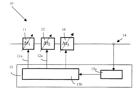
~0 for PMD in accordance with the present invention.
Best mode for Carrying Ov.t the Invention
With reference to Figure 2, an apparatus 10 for
mitigating or compensating for polarization mode dispersion
(PMD) in an optical fiber transmission system comprises a
?5 first and a second variable-DGD birefringent element,
designated as 11 and 12 respectively and connected in series,
a fixed-DGD element (third element) 16, connected in tandem
to the second variable-DGD element 12, a splitter 14 of known
type connected to the third element 16, and a feedback
>0 circuit 15 connected to the splitter 14.
The first and second variable-DGD birefringent elements
(first and second variable-DGD elements) 11 and 12 are of
known type and have birefringence axes that are not mutually
CA 02477682 2004-08-27
WO 03/073655 PCT/IT02/00158
6
parallel and a birefringence value selected on the basis of
the fiber PMD to be compensated.
The fixed-DGD element 16 has a birefringence axis that is
not parallel to the second variable-DGD element 12.
In accordance with a distinguishing feature of the present
invention, the first and second variable-DGD elements 11 and
12 and the fixed-DGD element 16 are capable of selectively
compensating for respective optical signal group delays, as
will be described in further detail below.
In particular, and in accordance with the principal feature
of the present invention, the concatenation of the three
birefringent elements (11, 12 and 16) as described, makes it
possible to vary all possible vectors of the principal
states of polarization (PSPs) as the DGD of the two variable-
DGD elements 11 and 12 varies, and thus to compensate for the
DGD introduced by the optical fiber while requiring only two
control variables for this purpose.
The feedback circuit 15 comprises a measuring element
15a in accordance with the prior art which is capable of
measuring the degree of distortion caused by the PMD of the
signal tapped by the splitter 14, and a control device 15b
connected in tandem to the measuring element 15a and capable
of dynamically sending control signals compensating for the
optical signal distortion measured by the measuring element
~5 15a to the first and second variable-DGD elements 11 and 12
by means of the associated control connections 11a and 11b.
Specifically, the control device 15b, which may for example
be based on a known microprocessor architecture, is capable
of generating DGD control signals of known type on the basis
of programs developed at the design stage for the apparatus
10 and stored in the control device 15b, and of transmitting
said signals selectively to the first and second variable-DGD
elements 11 and 12 by means of the respective connections 11a
and 12a in such a way as to compensate for the distortion
CA 02477682 2004-08-27
WO 03/073655 PCT/IT02/00158
7
caused by PMD as measured by the measuring element 15a in
accordance with a distinguishing feature of the present
invention.
In accordance with another embodiment of the invention,
the fixed-DGD birefringent element 16 may be replaced by a
variable-DGD birefringent element of known type controlled
via a connection 16a by the control device 15b and having a
birefringence axis which is not parallel to the second
variable-DGD element 12, in such a way as to obtain a
further degree of freedom in the PMD compensation process.
In this second embodiment, the fact that the DGD of the third
birefringent element 16 can also be varied improves the
apparatus's ability to track fluctuations in the optical
fiber's PSPs over time, though the introduction of a third
control variable leads to an increase in complexity.
The operating principle of the apparatus 10 as described
above is as follows.
The concatenation of the three birefringent elements 11,
12 and 16 of which at least two are variable constitutes a
'0 birefringent optical element characterised by a PSP vector
(direction and modulus in the Stokes space) which is a
function of the birefringence of the individual birefringent
elements.
In particular, the concatenation of the three birefringent
?5 elements 11, 12 and 16 makes it possible to obtain a PSP
vector of arbitrary direction by appropriately regulating the
DGD of the first two variable-DGD elements 11 and 12, and
thus to compensate for the fiber's PSP vector, whatever its
direction may be.
30 In the same way, the concatenation makes it possible to
compensate for the PSP vector modulus in a range of values
that depends on the DGD values for the individual
birefringent elements and which, as the result of a design
decision, must be sufficiently wide to ensure the
CA 02477682 2004-08-27
WO 03/073655 PCT/IT02/00158
8
compensation of all of the DGD values arising in succession
as the fiber's PMD fluctuates over time and which, in
general, are known or can be determined statistically.
In accordance with other embodiments of the invention,
additional variable-DGD and/or fixed-DGD elements can be
cascaded in modular fashion from the first three birefringent
elements 11, 12 and 16 in order to compensate for
differential group delays of higher order than those
considered here and measured by the measuring element 15a.
Naturally, the feedback circuit in these other embodiments of
the invention comprises a control connection for additional
variable-DGD elements and is capable of generating a single
further control signal for each additional variable-DGD
element.
Furthermore, the concatenation of several birefringent
elements, e.g., the three birefringent elements 11, 12 and
16, which are not mutually parallel, makes it possible to
generate a PSP vector which varies as a function of the
optical signal's frequency.
This variable PSP vector, which is, as is known, itself a
second-order PMD effect, makes it possible to compensate for
or at least mitigate the effects of the fiber's second-order
PMD.
Thanks to the architecture described, the feedback
circuit 15, as will be readily apparent to a person skilled
in the art, requires fewer control connections and
corresponding control signals than are needed in prior art
systems, both in order to compensate for the effects of
first- and second-order PMD, and to compensate for the
effects of higher-order PMD.
The dimension, forms, materials, components, circuit
elements and connections as contemplated in the foregoing
description are capable of modifications in various obvious
respects, as are the details of the circuitry and
CA 02477682 2004-08-27
WO 03/073655 PCT/IT02/00158
9
construction as illustrated and of the operating method, all
without departing from the scope of the invention as
specified in the appended claims.