Note: Descriptions are shown in the official language in which they were submitted.
CA 02478004 2004-08-18
37505.0366
USE OF PAD PRTNTING IN THE MANUFACTURE OF CAPACITORS
CROSS-REFERLNCE TO RELATED APPLICATION
This application claims priority from provisional
application Serial Nos. 60/495,967 and 60/495,980, both filed
August 18, 2003.
BACKGROUND OF THE INVENTION
1. Field of the Invention
The present invention generally relates to the production
of devices that convert chemical energy into electrical
energy. More particularly, the present invention relates to
pad printing processes for coating an electrode active reagent
solution or suspension on a conductive substrate. Preferably,
the reagent solution or suspension is of a cathode active
material, such as of a ruthenium-containing compound, for an
electrolytic capacitor. The ruthenium-containing compound is
provided as a printable ink comprising an aqueous or non-
aqueous carrier, and a binder, preferably a poly(alkylene)
carbonate binder. The present invention also relates to using
poly(alkylene) carbonates as a binder in a pressed valve metal
anode for an electrolytic capacitor.
2. Prior A.rt
Electrodes with high specific surface areas result in
specific capacitance in the hundreds of ~.~.F/cm2. Such
electrodes are then appropriate when used as the anode and/or
cathode in an electrochemical capacitor and as the cathode in
CA 02478004 2004-08-18
- 2 -
37505_0366
an electrolytic capacitor, which require high specific
capacitances.
An anode or cathode in an electrochemical capacitor or
the cathode in an electrolytic capacitor generally includes a
substrate of a conductive metal, such as titanium or tantalum,
provided with a pseudocapacitive oxide coating, nitride
coating, carbon nitride coating, or carbide coating. In the
case of a ruthenium oxide cathode, the active material is
formed on the substrate by coating a suspension or dissolved
solution of ruthenium oxide or a precursor thereof, such as
ruthenium chloride or ruthenium nitrosyl nitrate. The thusly-
coated substrate is then heated to a temperature sufficient to
evaporate the solvent and, if applicable, convert the
precursor, to provide a highly porous, high surface area
pseudocapacitive film of ruthenium oxide on the substrate.
The prior art describes various methods of contacting the
substrate with the pseudocapacitive reagent solution. For
example, Shah et al. and Muffoletto et al. in U.S. Patent Nos.
5,894,403, 5,920,455, 5,926,362, 6,224,985, 6,334,879 and
6,468,605, all of which are assigned to the assignee of the
present invention and incorporated herein by reference,
describe coating a ruthenium-containing reagent solution to a
conductive substrate by ultrasonic spraying. Ultrasonic
spraying is an imgrovement over other commonly used techniques
including dipping, pressurized air atomization spraying, and
deposition of a sol-gel onto the substrate. Capacitance
values for electrodes made by these latter techniques are
lower in specific capacitance than those made by ultrasonic
spraying. It is also exceptionally difficult to accurately
control the coating morphology due to the controllability and
repeatability of the dipping, pressurized air atomization
CA 02478004 2004-08-18
- 3 -
37505.0366
spraying, and sol-gel deposition techniques, which directly
impacts capacitance. While the coating morphology is
generally good with an ultrasonically spray deposited coating,
this technique has problems with overspray, which impacts
production costs, especially when the active material is
relatively expensive, such as ruthenium.
Therefore, while ultrasonically spraying an active
reagent solution onto a substrate is an improvement in
comparison to other known deposition processes that provide
capacitors with acceptable energy storage capacities, there is
a need to further improve production yields that are
negatively impacted by wasteful overspray. Increased
production yields result by coating an active reagent solution
or suspension onto a conductive substrate using a pad printing
technique.
SUN~iARY OF THE INVENTION
The present invention describes the deposition of a
metal-containing reagent solution or suspension onto a
conductive substrate by various pad-printing techniques. This
results in a pseudocapacitive oxide coating, nitride coating,
carbon nitride coating, or carbide coating having an
acceptable surface area commensurate with that obtained by
ultrasonically spraying, but with increased yields because
over-spray is not a concern. Other advantages include coating
thickness uniformity, better adhesion and sustained long-term
performance when stored at high temperature during accelerated
life test.
CA 02478004 2004-08-18
- 4 -
37505.0366
Tn a pad-printing process, the printing ink contains the
ruthenium-containing reagent dissolved or well dispersed in a
stable suspension. In either case., the system requires an
aqueous or non-aqueous carrier. The ink is printed onto a
conductive substrate that is then heated to evaporate the
solvent, remove the binder, and in some cases, convert the
reagent to the desired ruthenium compound. The binder is a
viscosity modifier to aid in processing the reagent ink and in
the pad printing process. Upon heating to evaporate the
solvent and, if applicable, convert the ruthenium-containing
precursor, to provide the desired ruthenium coating, the
binder burns off leaving very small quantities of residual
carbon. Excessive residual carbon effects performance of the
electrolytic capacitor.
The present poly(alkylene) carbonates are also useful as
binders in a dry pressed valve metal powder anode, such as of
pressed tantalum powder.
These and other objects of the present invention will
become increasingly more apparent to those skilled in the art
by a reading of the following detailed description in
conjunction with the appended drawings.
BRIEF DESCRIPTION OF THE DRAWINGS
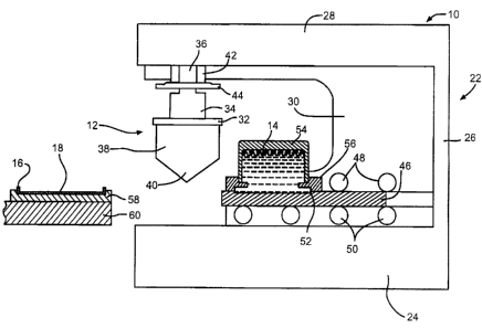
Fig. 1 is a schematic view of a first embodiment of a
sealed ink cup pad printing apparatus 10 of the present
invention showing a printing tampon 12, substrate 16, cliche
46 and reagent ink cup 54 prior to the start of a cycle.
CA 02478004 2004-08-18
- 5 -
37505.0366
Fig. 2 is a schematic view of the pad printing apparatus
with reagent ink 14 filled in the recess 52 of the cliche
and the printing tampon contacting the ink.
Fig. 3 is a schematic view of the pad printing apparatus
10 with the inked printing tampon positioned vertically above
the substrate 16.
Fig. 4 is a schematic view of the pad printing apparatus
10 with the inked printing tampon contacting the substrate.
Fig. S is a schematic view of the pad printing apparatus
10 before the inked substrate is moved to a further processing
step.
Fig. 6 is a perspective view of the inked substrate.
Fig. 6.A is a perspective view of the printing tampon.
Fig. 7 is a schematic view of a second embodiment of a
sealed ink cup pad printing apparatus 100 of the present
invention showing the printing tampon 12 positioned vertically
above the substrate 16 and with an ink cup 54 filling the
reagent ink into the recess 102 of a cliche 104 prior to the
start of a cycle.
Fig. 8 is a schematic view of the pad printing apparatus
100 with reagent ink 14 filled in the recess of the cliche and
the printing tampon positioned vertically above the ink.
Fig. 9 is a schematic view of the pad printing apparatus
100 with the printing tampon picking up the ink in the clich~
recess.
Fig. 10 is a schematic view of the pad printing apparatus
100 with the inked printing tampon positioned vertically above
the substrate.
Fig. 11 is a schematic view of the pad printing apparatus
100 with the inked printing tampon contacting the substrate.
CA 02478004 2004-08-18
- 6 -
37505.0366
Fig. 12 is a schematic view of the pad printing apparatus
100 before the inked substrate is moved to a further
processing step.
Fig. 13 is a schematic view of a third embodiment of a
sealed ink cup pad printing apparatus 110 of the present
invention showing the printing tampon 12 positioned vertically
above the recess 118 of a clich~ 116 prior to the start of a
cycle.
Fig. 14 is a schematic view of the pad printing apparatus
110 with reagent ink 14 filled in the clich~ recess and the
printing tampon positioned vertically above the ink.
Fig. 15 is a schematic view of the pad printing apparatus
110 with the printing tampon picking up the ink in the cliche
recess.
Fig. 16 is a schematic view of the pad printing apparatus
110 with the inked printing tampon positioned vertically above
the substrate.
Fig. 17 is a schematic view of the pad printing apparatus
110 with the inked printing tampon contacting the substrate.
Fig. 18 is a schematic view of the pad printing apparatus
110 before the inked substrate is moved to a further
processing step.
Fig. 19 is a schematic view of an open inkwell pad
printing apparatus 200 of the present invention showing a
printing tampon 12, substrate 16, cliche 202 and ink well 206
prior to the start of a cycle.
Fig. 20 is a schematic view of the pad printing apparatus
200 with reagent ink 14 filled in the recess 204 of the cliche
202 by a squeegee with excess ink being removed by a doctor
blade 212.
CA 02478004 2004-08-18
_ 7
37505.0366
Fig. 21 is a schematic view of the pad printing apparatus
200 with the printing tampon 12 contacting the ink.
Fig. 22 is a schematic view of the pad printing apparatus
200 with the inked printing tampon 12 positioned vertically
above the substrate 16.
Fig. 23 is a schematic view of the pad printing apparatus
200 with the inked printing tampon 12 contacting the substrate
16.
Fig. 24 is a schematic view of a rotary gravure pad
printing apparatus 300 showing a cliche drum 304 picking up a
reagent ink 14 from a well 302 for transfer to a main roller
306 and ultimately to substrates located on a substrate wheel
308.
Fig. 25 is a schematic view of the rotary gravure pad
printing apparatus 300 with the reagent ink 14 being
transferred from the clich~ drum 304 to the main roller 306.
Fig. 26 is a schematic view of the rotary gravure pad
printing apparatus 300 with the reagent ink 14 contacted to
the main roller 306.
Fig. 27 is a schematic view of the rotary gravure pad
printing apparatus 300 with the reagent ink 14 being
transferred from the main roller 306 to substrates located on
a substrate wheel 308.
Fig. 28 is a graph constructed from the average energy
delivered by tantalum capacitors having cathodes of pad
printed ruthenium oxide heated to various final temperatures.
Fig. 29 is a graph of weight loss versus heating
temperature for a polypropylene carbonate) binder.
Fig. 30 is an x-ray diffraction scan of ruthenium oxide
pad printed according to the present invention and heated to
various final temperatures.
CA 02478004 2004-08-18
_ g
37505.0366
Fig. 31 is a graph of the average specific capacitance of
ruthenium oxide coated titanium substrates heated to various
temperatures and calculation of the hypothetical capacitance
of an electrolytic capacitor.
Figs. 32 and 33 are backscatter images of ruthenium oxide
coated on a titanium substrate by a pad printing process and
ultrasonically spray coated on a titanium substrate according
to the prior art, respectively.
DETAILED DESCRIPTION OF THE PREFERRED EMBODIMENTS
The present invention will be described with respect to
various pad-printing techniques for depositing or coating
reagent ink containing an active material, or precursor
thereof, onto a substrate. The pad printing techniques
include those performed by sealed ink cup pad printing, open
inkwell pad printing and rotary gravure pad printing.
Turning now to the drawings, Figs. 1 to 5 illustrate a
first embodiment of a sealed ink cup pad printing apparatus 10
using a printing tampon 12 (Fig. 6A) for precisely and evenly
contacting an ink 14 of a reagent solution or suspension to a
substrate. The substrate can be planar or a shaped member as
a casing portion 16 (Fig. 6). The reagent ink solution or
suspension is made up of an aqueous or non-aqueous carrier and
an organic binder. Suitable solvents include terpineol
(boiling point = 220°C), butyl carbitol (b. p. - 230°C),
cyclohexanone (b. p. - 155.6°C), n-octyl alcohol (b. p. -
171°C),
ethylene glycol (b.p. - 197°C), glycerol (b.p. - 290°C) and
water. These are relatively high bonding point solvents that
CA 02478004 2004-08-18
_ g _
37505.0366
do not evaporate at room temperature and maintain rheology or
viscosity during printing.
Suitable salts and dispersible compounds include
nitrates, sulfates, halides, acetates, and phosphates to
produce the active material being an oxide, nitride, carbide
or carbon nitride of ruthenium, cobalt, manganese, molybdenum,
tungsten, tantalum, iron, niobium, iridium, titanium,
zirconium, hafnium, rhodium, vanadium, osmium, palladium,
platinum, nickel, and Lead.
A preferred reagent precursor for a ruthenium oxide
coating is a ruthenium halide, ruthenium nitrate, ruthenium
acetate, or ruthenium sulfate, or an organic salt. In that
respect, suitable precursors include the soluble salts of
ruthenium(III) chloride hydrate, ruthenium(III) nitrosyl
nitrate, nitrosyl ruthenium(III) acetate, ruthenium(TII)
nitrosylsulfate, and ammonium hexachlororuthenium(III). These
miscible precursors are capable of being mixed in the above
solvents in any ratio without separation into two phases.
Ruthenium dioxide on the hand forms a dispersion with these
solvents, which precludes use of the precursor compounds.
The reagent solution may include a second or more metals.
The second metal is in the form of an oxide, or precursor
thereof. The second metal is selected from one or more of the
group consisting of tantalum, titanium, nickel, iridium,
platinum, palladium, gold, silver, cobalt, molybdenum,
manganese, tungsten, iron, zirconium, hafnium, rhodium,
vanadium, osmium, niobium, and mixtures thereof. In a
preferred embodiment of the invention, the reagent solution
comprising the ink 14 includes oxides of ruthenium and
tantalum, o:r precursors thereof.
CA 02478004 2004-08-18
- 10 -
37505_0366
The reagent ink 14 is preferably at a concentration of
from about 150 to about 500 grams of the reagent compounds per
liter.
The reagent ink 14 further includes a binder. Suitable
binders include ethyl cellulose, acrylic resin, polyvinyl
alcohol, polyvinyl butyral and a poly(alkylene carbonate)
having the general formula R-O-C(=0)-O with R = Cl to C5.
Polyethylene carbonate) and polypropylene carbonate) are
preferred. It is critical to use a very low ash content
binder in electrical energy storage systems. Poly(alkylene
carbonate) binders burn out of the reagent ink in any
atmosphere including nitrogen, air, hydrogen, argon and
vacuum, leaving only very small quantities of carbon (6.9 ppm
per ASTM D482). Suitable poly(aklylene carbonate) binders are
commercially available from Empower Materials, Inc., Newark,
Delaware under the designations QPAC 25 and QPAC 40.
The substrate 16 preferably consists of a conductive
metal such as titanium, molybdenum, tantalum, niobium, cobalt,
nickel, stainless steel, tungsten, platinum, palladium, gold,
silver, copper, chromium, vanadium, aluminum, zirconium,
hafnium, zinc, iron, and mixtures and alloys thereof, and
comprises a bottom wall 18 supporting a surrounding sidewall
20 forming an opening leading therein. It is through this
opening that the printing tampon 12 moves to deposit the
reagent ink 14 onto of the substrate casing portion 16 in a
specifically designed pattern dictated by the capacitor (not
shown) to be constructed. In general, the thickness of the
substrate is in the range of about O.OOI millimeters to about
2 millimeter, and preferably about 0.1 millimeters.
Regardless of the material of the substrate 16, coating
integrity relies mostly upon mechanical bonding to the
CA 02478004 2004-08-18
- 11 -
37505.0366
contacted surface. It is, therefore, critical that the
substrate 16 is properly prepared to ensure coating quality.
For one, substrate surface cleanliness is very important in
all coating systems. In that respect, it is required that the
substrate 16 remain uncontaminated by lubricants from handling
equipment or body oils from hands, and the like. Substrate
cleaning includes chemical means such as conventional
degreasing treatments using aqueous and non-aqueous solutions
as are well known tv those skilled in the art. Plasma
cleaning is also used.
After substrate surface cleaning, surface roughness is
the next most critical factor for coating adhesion. The
bottom wall 18 may be roughened by chemical means, for
example, by contacting the substrate with hydrofluoric acid
and/or hydrochloric acid containing ammonium bromide and
methanol, and the like, by plasma etching, and by mechanical
means such as scraping, machining, wire brushing, rough
threading, grit blasting, a combination of rough threading
then grit blasting and abrading such as by contacting the
substrate with Scotch-Brite~ abrasive sheets manufactured by
3M.
zf desired, the electrical conductivity of the substrate
16 is improved prior to coating. Metal and metal alloys
naturally have a native oxide on their exposed surfaces. This
is a resistive layer and hence, if the material is to be used
as a substrate for a capacitor electrode, the oxide is
preferably removed or made electrically conductive prior to
deposition of an active coating thereon. In order to improve
the electrical conductivity of the substrate 16, various
techniques can be employed. One is shown and described in
U.S. Patent No. 6,740,420 to Muffoletto et al., which is
CA 02478004 2004-08-18
- 12 -
37505.0366
assigned to the assignee of the present invention and
incorporated herein by reference.
The sealed ink cup pad printing apparatus 10 comprises a
main frame 22 having a platform 24 to which is fixed a
vertical support beam 26 and a cantilevered arm 28. A
generally C-shaped plate 30 is secured to the platform,
vertical beam and cantilevered arm to add support to the main
frame. The printing tampon 12 depends from the cantilevered
arm 28 for actuation in a relative upwardly and downwardly
vertical direction towards and away from the arm.
The printing tampon 12 comprises a backing plate 32
detachably secured to a piston 34 at the distal end of a
piston rod 36. The printing tampon 12 is more clearly shown
in Fig. 6A comprising the backing plate 32 supporting a
polymeric main body 38 provided with an extending pad portion
40. The pad portion 40 is shown as a curved surface, but when
it is deformed by contact with the substrate 16, it assumes
the desired peripheral shape.
The piston rod 36 resides in a closely spaced
relationship in a cylinder 42 that precisely controls the axis
of vertical movement of the piston 34 and attached printing
tampon 12. A limit plate 44 is secured to the piston rod 36
adjacent to the piston 34. This ensures that the piston does
not retract upwardly too far to be damaged by a collision with
the C-shaped plate 30 and cantilevered arm.
The mainframe platform 24 supports a cliche 46 that
actuates in a back and forth manner on a series of upper and
lower bearings 48 and 50, respectively. The cliche 46 is a
plate shaped metal member, such as of A2 tool steel coated
with a diamond like carbon finish. The cliche has a
chemically etched recess 52 sized to create the image or
CA 02478004 2004-08-18
- 13 -
37505.0366
perimeter of the reagent ink 14 to be deposited on the
substrate 16. A cup 54 containing the reagent ink 14 is
supported on the cliche 46 by a magnetic sealing ring 56. The
magnetic attraction between the cliche and ring provides a
closely spaced tolerance that squeegees the reagent ink 14
filled into the recess 52 to a precise depth. The reagent ink
14 is now ready for subsequent transfer to the printing tampon
12 as the cliche 46 travels back and forth. This will be
described in greater detail hereinafter.
As shown in Fig. 1, the sealed ink cup printing process
according to this first embodiment of the present invention
begins with the substrate 16 resting on a block 58 that may be
thermally conductive, which in turn is supported on a work
stage 60. The work stage 60 is preferably temperature
controlled and provides for movement of the block 58. In that
manner, the block conducts heat to the substrate 16 to
maintain it at a temperature sufficient to solidify and, if
applicable, convert the reagent ink to the desired active
material. The block 58 can also be left at ambient for room
temperature processing. For a more detailed description of
this heating and conversion process, reference is made to the
previously ~3iscussed U.S. Patent Nos. 5,894,403, 5,920,455,
5,926,362, 6,224,985, 6,334,879 and 6,468,605.
Alternatively, a conductive substrate (not shown) that is
not a casing portion is supported on the conductive block. In
that case, the conductive substrate will be generally planar
and contacted to the casing portion after being coated with
the reagent ink converted to the solidified active material,
as will be described in detail hereinafter with respect to
Figs. 24 to 27.
CA 02478004 2004-08-18
- 14 -
37505.0366
As shown in the drawing of Fig. 1, a pad printing cycle
of the first embodiment begins with the clich~ 46 in a
retracted position having its recess 52 directly aligned with
the ink cup 54 magnetically sealed thereto by the ring 56.
In Fig. 2, the clich~ has moved to the left such that the
reagent ink 14 filled in the recess 52 is completely free of
the ink cup 54 and in a precise vertical alignment with the
retracted printing tampon 12. The piston 34 is then actuated
to move the printing tampon 12 in a downwardly direction to
have the extended pad portion 40 contact and pick up the ink
14 onto its printing surface, As previously discussed, the
extending pad portion 40 has a curved surface, which helps
prevent splashirig the ink 14 as the printing tampon 12 is
moved into contact with the substrate. In that respect,
downward actuation of the printing tampon 12 continues until
the pad portion 40 has deformed into the recess 52 to pick up
the reagent ink 14 deposited therein.
As shown in Fig. 3, the inked printing tampon 12 then
retracts into a raised position as the cliche 46 is
simultaneously retracted away from vertical alignment with the
substrate 16. The recess 52 of the clich~ 46 is once again
aligned with the ink cup 54 for filling another charge of
reagent ink therein. As this occurs, the work stage 60 is
simultaneously actuated to move into a position with the
conductive block 58 supporting the substrate 16 directly
aligned beneath the inked printing tampon 12.
In Fig. 4, the printing tampon 12 is actuated in a
downwardly direction to contact the bottom wall 18 of the
substrate 16 with its inked pad portion 40. As this occurs,
the pad portion 40 deforms to completely contact the area of
the substrate bottom wall 18 to be coated with the reagent
CA 02478004 2004-08-18
- 15 -
37505.0366
ink. The surface tension of the reagent ink contacting the
bottom wall 18 is greater than the surface tension of the ink
contacting the pad portion 40 of the printing tampon. In that
manner, the reagent ink 14 is deposited onto the casing
portion bottom wall 18 when the printing tampon 12 moves into
the retracted position of Fig. 5. The work stage 60 also
retracts into its starting position.
During deposition of the reagent ink 14 onto the bottom
wall 18 of the substrate 16, the conductive block 58 and work
stage 60 maintain the substrate at a temperature sufficient to
evaporate or otherwise drive off the solvent from the
deposited reagent mixture. In addition, printing can be done
at ambient temperature and with solvent removal performed in a
subsequent process. As will be described in detail
hereinafter, the coated substrate is then subjected to a
separate heating step to convert the precursor to the oxide
and to diffuse the deposited ions into the substrate for
proper bonding or adhesive strength. This heating step is in
addition to heating the substrate to evaporate the solvent.
Thus, as the casing portion 16 is being coated with the
reagent ink, the bottom wall 18 is at a temperature sufficient
to begin driving off or otherwise evaporating the solvent
material. If desired, this can be performed at ambient.
Preferably, the solvent is evaporated from the substrate 16
almost instantaneously with contact by the reagent ink 14
resulting in deposition of a relatively thin film coating of
the cathode active material, or precursor thereof. In the
case of an aqueous solution, the substrate is heated to a
first temperature of at least about 100°C to instantaneously
evaporate the solvent from the deposited reagent solution.
More preferably, as the deposition of the reagent ink is
CA 02478004 2004-08-18
- 16 -
37505.0366
taking place, the substrate is heated to the first temperature
of up to about 220°C. A higher first temperature results in a
greater solvent evaporation rate. A thin film is defined as
one having a thickness of about 1 micron and less.
Tn the case where the product active material is intended
to be a ruthenium-containing oxide compound, the deposited
nitrate, sulfate, acetate, chloride, or phosphate precursor is
heated to a temperature sufficient to burn off the binder and
convert the reagent ink to a highly porous, high surface area
pseudocapacitive film. Typical heating times are from about
five minutes to about six hours.
For example, after deposition and solvent removal, the
precursor-coated substrate is heated to a second temperature
of about 300°C to about 500°C, preferably about 350°C,
for at
least about five minutes to about three hours. A final
heating temperature of at least about 300°C is preferred to
substantially completely decompose and burn off the binder
from the pseudocapacitive film. Residual binder by-products
are known to affect capacitance in a negative manner.
This is only one heating protocol for converting a
reagent precursor to a ruthenium-containing oxide. It is
contemplated that ruthenium-containing oxides may be formed by
a step heating protocol, as long as the last heating is at
least about 300°C, and more preferably about 350°C, for at
least about five minutes.
Alternatively, after the initial deposition heating, the
temperature of the substrate 16 is slowly and steadily ramped
up, for example, at about 1°Clminute, preferably about 6°Clmin.
until the temperature reaches at least about 300°C to about
500°C, and more preferably about 350°C. The substrate is then
maintained at the maximum temperature for a time sufficient to
CA 02478004 2004-08-18
- I7 -
37505.0366
allow conversion of the precursor to its final form as a
ruthenium-containing oxide and to sufficiently diffuse the
active material into the substrate 16. Heating at 300°C, and
more preferably at about 350°C is for about five minutes or
longer.
In another embodiment; the substrate 16 is maintained at
a temperature sufficient to, for all intents and purposes,
instantaneously convert the precursor to a porous, high
surface area product active coating on the substrate. More
particularly, as the precursor reagent ink is deposited, the
substrate is at a temperature of about 100°C to about 500°C,
preferably .~t least about 200°C, and mare preferably about
300°C, and still more preferably about 350°C, to
instantaneously convert the precursor to the desired product.
The coating is heated for an additional time to ensure
complete conversion and binder burn out.
The decomposition temperature is about 220°C for the
previously described polyethylene carbonate) binder and about
250°C for the polypropylene carbonate) binder. Therefore,
the minimum final heating temperatures must exceed these
temperature: to ensure complete combustion of the binder into
non-toxic by-products, primarily of carbon dioxide and water.
After deposition and conversion of the precursor to the
product active coating, whether it is instantaneous or
otherwise, the substrate 18 is ramped down or cooled to
ambient temperature, maintained at the heated deposition
temperature to enhanced bonding strength, or varied according
to a specific profile. In general, it is preferred to conduct
the heating steps.while contacting the substrate with air or
an oxygen-containing gas.
CA 02478004 2004-08-18
37505.0366
- 18 -
In the case of a product porous ruthenium-containing
oxide, it is preferred that the resulting coating have a
thickness of from about a hundred Angstroms to about 0.1
millimeters, or more. The porous coating has an internal
surface area of about 1 m2/gram to about 1,500 mZ/gram. Also,
a majority of the particles of the porous coating have
diameters of less than about 500 nanometers.
While not shown in the drawings, the inked substrate 16
is removed from the conductive block 58 and heated work stage
60 for further processing into an electrical energy storage
device, such as a capacitor. A second substrate is then
positioned on the conductive block and the cycle is repeated.
Figs. 7 to 12 illustrate a second embodiment of a sealed
ink cup pad printing apparatus 100 according to the present
invention. This apparatus includes many of the same
components as the apparatus 10 described with respect to Figs
1 to 5, and like parts will be provided with similar numerical
designations.
As particularly shown in Fig. 7, the sealed ink cup pad
printing apparatus 100 comprises the main frame 22 having the
platform 24 fixed to the vertical beam 26 supporting the
cantilevered arm 28. In this embodiment, the printing tampon
12 is not only actuatable in an upwardly and downwardly
direction, it is also movable in a forwardly and backwardly
direction with respect to the cantilevered arm 28. However,
in this embodiment instead of the cliche actuating in a back
and forth manner, the ink cup 54 does. In that light, Fig. 7
shows the ink cup 54 aligned with the recess 102 of the
stationary cliche 104 to deposit a change of the reagent ink
14 therein. The printing tampon 12 is in a retracted position
CA 02478004 2004-08-18
- 19 -
37505.0366
aligned vertically above the substrate 16 supported on the
substrate 5:3 and work stage 60.
In Fig. 8, the ink cup 54 has retracted along the cliche
104 and away from its recess 3.02 with a charge of reagent ink
14 deposited therein. Likewise, the printing tampon 12 has
moved along the cantilevered arm 28 a like distance as the ink
cup 54 has moved along the stationary cliche 104. The
printing tampon 12 is now positioned vertically above the
reagent ink 14 deposited in the cliche recess 102.
Fig. 9 illustrates the printing tampon 12 having been
actuated in a downwardly direction with the pad portion 40
contacting the clich~ 104 to pick up the reagent ink 14
contained in the recess thereof. The inked printing tampon 12
then retracts into a raised position as the ink cup 54 is
simultaneously actuated into alignment with the recess 102 in
the cliche 104 to once again deposit a charge of reagent ink
therein. As in the simultaneous movement described. in Fig. 8,
the printing tampon 12 and ink cup 54 have each moved a like
distance in a reverse direction in Fig. 10. The printing
tampon 12 is now vertically aligned with the substrate 16
supported on the conductive block 58 and heated work stage 60.
Fig. 11 illustrates the printing tampon 12 having been
actuated in a downwardly direction to contact the substrate
16. As this occurs, the pad portion 40 deforms to completely
contact the area of the substrate bottom wall 18 to be coated
with the reagent ink. In that manner, the reagent ink 14 is
deposited onto the casing bottom wall 18 when the printing
tampon 12 moves into the retracted position of Fig. 12_ The
inked substrate 16 is then removed from the conductive block
58 and heatEd work stage 60 for further processing into an
electrical energy storage device. A second substrate is
CA 02478004 2004-08-18
- 20 -
37505.0366
positioned on the substrate and the pad printing cycle process
is repeated.
Figs. 13 to 18 illustrate a third embodiment of a sealed
ink cup pad printing apparatus 110 according to the present
invention. This apparatus includes many of the same
components as the apparatuses 10 and 100 described with
respect to Figs. 1 to 5 and 7 to 12, respectively, and like
parts will be provided with similar numerical designations.
As particularly shown in Fig. 13, the pad printing
apparatus 110 comprises a main frame 112 supporting a housing
114 for the piston 34 and piston rod 36 actuatable in an
upwardly and downwardly direction along a cylinder 42. A
limit plate 44 ensures that the piston 34 does not retract
upwardly too far to collide with the housing 114. A printing
tampon 12 is detachably secured to the end of the piston 36 by
a backing plate 32.
A cliche 116 is connected to the main frame 112 and
serves as a stage for backward and forward movement of the ink
cup 54 there along. The ink cup 54 is sealed to the cliche
116 by a squeegee ring 56. The cliche 126 includes a recess
118 so that as the ink cup 54 travels back and forth along the
cliche 116, the reagent ink 14 is precisely filled into the
recess 118 (Fig. 14) for subsequent transfer to the printing
tampon 12.
As shown in Fig. 15, once the cliche recess 118 is filled
with the reagent ink 14 and the ink cup 54 has moved to a
position free of the printing tampon 12, the piston 34 is
actuated in a downwardly direction. This moves the printing
tampon in a downwardly direction to contact the cliche 116 and
pick up the reagent ink 14 onto its extended pad portion 40.
The inked printing tampon 12 then retracts into a raised
CA 02478004 2004-08-18
- 21 -
37505.0366
position. 'rhe printing tampon 12 is next actuated in a
forwardly direction and into vertical alignment with the
substrate 16 supported on the conductive block 58 and heated
work stage 60. This positioning is shown in Fig. 16.
Fig. 17 illustrates the printing tampon 12 having been
actuated in a downwardly direction to contact the substrate
16. The pad portion 40 deforms to completely contact the area
of the casing bottom wall 18 to be coated with the reagent
ink. In that manner, the reagent ink 14 is deposited onto the
casing bottom wall 18 when the printing tampon l2 moves into
the retracted position of Fig. 18. The inked substrate 16 is
then removed from the conductive block 58 and heated work
stage 60 for further processing into an electrical energy
storage device. A second substrate is positioned on the
conductive block, and the recess 118 in the cliche 116 is once
again preci:~ely filled with the reagent ink 14 as the ink cup
54 and seal 56 travel along the cliche 116 to the position
shown in Fig. 13. The printing tampon 12 then cycles to pick
up the ink and deposit it onto the substrate as previously
described.
Tn that manner, a cycle of the pad printing apparatus 110
is not complete until the ink cup 54 has traveled back and
forth across the cliche 116, filling the recess 118 each time.
This benefits cycle time as each movement of the ink cup 54
across the cliche 116 results in an inked substrate.
Figs. :l9 to 23 illustrate a further embodiment of the
present invention using an open inkwell pad printing apparatus
200 according to the present invention. The open inkwell pad
printing apparatus 200 comprises a cliche 202 having a recess
204 and an inkwell 206 containing reagent ink 14. Mounted
vertically above the clich~ 202 is a support beam 208 that
CA 02478004 2004-08-18
- 22 -
37505_0366
provides for vertical translation of the printing tampon 12, a
squeegee 210 and a doctor blade 212. The squeegee is
connected to the support beam by a depending beam 214 having a
first actuatable pivot member 216. A secondary arm 218 is
axially movable with respect to a rod 220 connected to the
pivot member 216. A second actuatable pivot member 222 is at
the distal end of the secondary arm 218 and supports the
squeegee 210 for rotational movement into and out of contact
with the cliche 202.
A horizontal beam 224 is connected to the depending beam
214 with the doctor blade 212 pivotably supported at the
distal end of the horizontal beam 224. An actuatable arm 226
connects between the support beam 208 and the secondary arm
218 for precise pivotable movement of the doctor blade 212
into and out of contact with the cliche 202.
As shown in Fig. 19, a pad printing cycle using the open
inkwell printing apparatus 200 begins with a quantity of
reagent ink 14 filled into the well 206 located in the cliche
202. The squeegee 210 is moved across the inkwell 206 to move
a volume of reagent ink 14 onto the upper surface of the
cliche 202. The reagent ink 14 flows into the recess 204 as
the squeegee travels to the left. After the recess is filled,
the doctor blade 212 is moved back over the recess toward the
right to skim any excess reagent ink 14 back into the inkwell
206. This provides a precise quantity of reagent ink filled
into the recess 204.
In Fig. 21, the squeegee 210 and doctor blade 212 are
pivoted out of contact with the cliche 202. This helps
prevent wear. In this drawing, the tampon 12 has also moved
in a downwardly direction so that the extended pad portion 40
contacts and picks up the reagent ink 14 onto its printing
CA 02478004 2004-08-18
- 23 -
37505.0366
surface. The inked printing tampon 12 is then retraced and
moved into a raised position directly above the substrate 16
(Fig. 22). Fig. 23 shows the printing tampon 12 having been
actuated in a downwardly direction to contact the bottom wall
18 of the substrate with its inked pad portion 40. As the pad
portion deforms, it completely contacts the area of the
substrate 16 to coat the reagent ink thereon. As previously
described, the conductive block 58 and workstation 60 maintain
the substrate at the desired temperature. The inked substrate
16 is then removed from the conductive block 58 and heated
work stage 60 for further processing into an electrical energy
storage device. A second substrate is positioned on the
conductive block and the cycle is repeated.
Figs. 24 to 27 illustrate a further embodiment of a
rotary gravure pad printing apparatus 300. This apparatus
comprises an inkwell 302 containing reagent ink, a cliche in
the form of a rotating drum 304, a main roller 306 and a
substrate wheel 308. While not shown in the drawings, the
wheel 308 supports a plurality of substrates that will
subsequently be processed into electrical energy storage
devices according to the present invention.
Fig_ 24 shows the clich~ drum 304 rotating with its
surface immFrsed in the inkwell 302 to fill the reagent ink 14
into recesses 310 spaced along its surface. A squeegee 312 is
in the form of a fork having legs supported on the inkwell on
opposite sides of the drum 304. An intermediate portion
between the legs wipes excess reagent ink from the cliche drum
304 so that a precise quantity of reagent ink is filled in the
recesses 310.
In Fig. 2S, the main drum 306 has moved into contact with
the cliche drum 304. The main drum 306 is provided with a
CA 02478004 2004-08-18
- 24 -
37505.0366
release contact surface 306A, preferably of silicone, that
enables the reagent ink 14 to transfer from the cliche
thereto, as shown in Fig. 26. The rotating substrate wheel
308 moves into contact with the main drum 306 so that the
reagent ink 14 is deposited onto substrates fnot shown)
carried thereon. In this embodiment, the substrates are plate
shaped members that are heat processed as previously described
and then supported on the bottom wall 18 of the substrate 16
shown in the previous drawings.
The anode electrode of the electrolytic capacitor is
typically of a valve metal selected from the group consisting
of tantalum, aluminum, titanium, niobium, zirconium, hafnium,
tungsten, molybdenum, vanadium, silicon and germanium, and
mixtures thereof in the form of a pellet. This is done by
compressing the valve metal in powdered form, for example
tantalum powder, into a pellet having an anode lead exr_ending
therefrom, and sintering the pellet under a vacuum at high
temperatures. Preferably, one of the previously described
binders, preferably a polyfalkylene carbonate), is used to
promote cohesion with the pressed powder body_ The binder
adds green strength to the pressed body and helps with powder
flow before pressing. For tantalum, the powder material can
be provided by either the beam melt process or the sodium
reduction process, as is well known to those skilled in the
art.
Regardless of the process by which the valve metal powder
was processed, pressed valve metal powder structures, and
particularly tantalum pellets, are typically anodized to a
desired voltage in formation electrolytes consisting of
ethylene glycol or polyethylene glycol, de-ionized water and
H3P04. These formation electrolytes have conductivities of
CA 02478004 2004-08-18
_ 25 _
37505.0366
about 250 ~.~.5/cm to about 2, 600 )..~.5/cm at 40°C. The other main
type of formation electrolyte is an aqueous solution of H3P04.
This type of electrolyte has conductivities up to about 20,000
~.S/cm at 40"C. Anodizing serves to fill the pores of the
pressed valve metal body with the electrolyte and to form a
continuous dielectric oxide film on the sintered body.
Anodizing produces an oxide layer over the terminal lead/anode
lead weld.
The anode can also be of an etched aluminum or titanium
foil or, a sintered aluminum or titanium body.
A separator structure of electrically insulative material
is provided between the anode and the cathode to prevent an
internal electrical short circuit between the electrodes. The
separator material also is chemically unreactive with the
anode and cathode active materials and both chemically
unreactive with and insoluble in the electrolyte. In
addition, the separator material has a degree of porosity
sufficient to allow flow therethrough of the electrolyte
during the electrochemical reaction of the capacitor.
Illustrative separator materials include woven and non-woven
fabrics of polyolefinic fibers including polypropylene and
polyethylene or fluoropolymeric fibers including
polyvinylidene fluoride, polyethylenetetrafluoroethylene, and
polyethylenechlorotrifluoroethylene laminated or superposed
with a polyolefinic or fluoropolymeric microporous film, non-
woven glass, glass fiber materials and ceramic materials.
Suitable microporous films include a polyethylene membrane
commercially available under the designation SOLUPOR (DMS
Solutech), a polytetrafluoroethylene membrane commercially
available under the designation ZITEX (Chemplast Inc.),
CA 02478004 2004-08-18
- 26 -
37505.0366
polypropylene membrane commercially available under the
designation CELGARD (Celanese Plastic Company, Inc.) and a
membrane commercially available under the designation DEXIGLAS
(C. H. Dexter, Div., Dexter Corp.). Cellulose based
separators also typically used in capacitors are contemplated
by the scope of the present invention. Depending on the
electrolyte used, the separator can be treated to improve its
wettability.
The anode and cathode electrodes are operatively
associated with each other by an electrolyte solution tilled
in the casing through an electrolyte fill opening. Any
electrolyte that is known for use with the particular anode
and cathode active materials selected to provide acceptable
capacitive performance over a desired operating range is
contemplated by the scope of the present invention. Suitable
electrolytes include sulfuric acid in an aqueous solution.
Specifically, a 38~ sulfuric acid solution performs well at
voltages of up to about 125 volts. A 10~ to 20~ phosphoric
acidlwater solution is known to provide an increased
equivalent series resistance (ESR) and breakdown voltage.
Other suitable electrolytes are described in U.S. Patent Nos.
6,219,222 to Shah et al. and 6,687,117 tv Liu et al. These
patents are assigned to the assignee of the present invention
and incorporated herein by reference.
The following examples describe capacitors made by a pad
printing process according to the present invention, and set
forth the best mode contemplated by the inventors of carrying
out the invE:ntion.
EXAMPLE I
CA 02478004 2004-08-18
- 27 -
37505.0366
One hundred fifty titanium substrates as casing portions
similar to substrate 16 in the drawing figures were coated
with an active ruthenium dioxide material by a closed inkwell
pad printing process according to the present invention. The
ink was a suspension of ruthenium dioxide and polyvinyl
butyral binder in a solvent mixture of terpineol and butyl
carbitol. The coated substrates were then divided into three
groups of fifty substrates apiece. The first group was heated
to a maximum temperature of 200°C, the second group was heated
to 300°C and the third group was heated to 400°C.
Test capacitors were then constructed from the processed
cathode substrates. Each capacitor comprised a pressed and
anodized tantalum powder anode positioned between two mating
casing portions containing ruthenium oxide cathode coatings
heated to the same final temperature. An electrolyte was
filed into the sealed casing to contact the anode and the
cathode, which were segregated from each other by a separator.
This resulted in three groups of twenty-five capacitors. Each
capacitor was charged to about 215 volts and discharged into a
16.5-ohm resistor once every 14 days. In the interim they
were stored at 85°C.
Fig. 28 is a graph constructed from the average energy
delivered by each capacitor in a group. In particular, curve
400 is the average of the capacitors containing the cathodes
heated to 200°C, curve 402 is the average of the capacitors
containing the cathodes heated to 300°C and curve 404 is the
average of the capacitors containing the cathodes heated to
400°C. It is clear that the final heating temperature of the
pad printed ruthenium oxide cathode material is critical in
the energy efficiency of the capacitors. It is believed that
CA 02478004 2004-08-18
- 28 -
37505.0366
300°C is the temperature at which the polypropylene carbonate)
binder completely decomposes into harmless carbon dioxide and
water.
EXAMPLE II
Fig. 29 is a graph showing the weight loss versus heating
temperature for a polypropylene carbonate) binder. Curve 410
is constructed from the binder heated in air, curve 412 is
from the binder heated in hydrogen, curve 414 is from the
binder heated in a vacuum (1 Torr) and curve 416 is from the
binder heated in nitrogen. It can be seen that substantially
all of the weight loss occurs prior to heating at about 300°C.
EXAMPLE III
Substrates pad printed in a similar as those used to
construct the capacitors of the three groups used in Example I
were heated to 250°C, 300°C, 350°C and 450°C,
respectively. The
substrates were then subjected to an x-ray diffraction (xRD)
analysis. The results are shown in Fig. 30. This XRD graph
is indicative of the crystallinity of the ruthenium oxide
active material. The higher peaks indicate a more crystalline
material. It is clear that the ruthenium oxide material
heated to a final temperature of 250°C is not as crystalline as
the other materials heated to higher temperatures.
CA 02478004 2004-08-18
- 29 -
EXAMPLE IV
37505.0366
For applications where a coated substrate is intended for
use in a supercapacitor (a capacitor where a metal oxide, for
example ruthenium dioxide, serves as both cathode and anode),
it is important that the specific capacitance is maximized.
However, for applications where a ruthenium oxide coated
substrate serves as the cathode in an electrolytic hybrid
capacitor, such as one having a pressed powder tantalum anode,
this is not critical since the anode dominates system
performance.
Assuming an electrolytic capacitor is constructed having
a tantalum anode with a capacitance Ca of 1 mF and a cathode
containing 2.7178 mg of the ruthenium dioxide. This mass
results in a cathode capacitance of C~ = 1 mF at 250°C. This
electrolytic capacitor can be modeled as a system of an anode
and a cathode capacitor in series. The resulting capacitance
of such an electrolytic capacitor can be calculated using the
formula C = Ca*C~l tCa+C~) . Curve 420 in Fig. 31 is the
capacitance calculation of this hypothetical electrolytic
capacitor.
Capacitors were constructed containing substrates pad
printed in a similar manner as those used to construct the
capacitors in Example I. The cathodes were heated to the
temperatures indicated in the abscissa in Fig 31. Decreased
capacitance at higher anneal temperatures is a well-
established fact. The temperature dependence of the
capacitance of these electrolytic capacitors based on the
anneal temperature of the cathode is designated by curve 422
in Fig. 31. It is essentially a horizontal line. The insert
figure is a magnified view showing that for this example using
CA 02478004 2004-08-18
37505.0366
- 30 -
a temperature of 350°C instead of 250°C decreases the overall
capacitance from 0.999 F to 0.996 F. This is a decrease of
0.3~. Most electrolytic capacitors only use a small amount of
cathode material and using more cathode active material can
compensate for a non-optimal specific capacitance.
EXAMPLE V
Substrates pad printed in a similar as those used to
construct the capacitors in Example I were heated to 350°C.
The capacitors were then subjected to shock and vibration
testing. Vibration test consisted of subjecting a capacitor
to random vibration in each of three orthogonal axes with the
following levels: 10 Hz: 0.03 G2/Hz, 40 Hz: 0.03 GZ/Hz, 500 Hz:
0.0003 G~/H::, for 1 hour per axis. Shock testing consisted of
subjecting a capacitor to a shock pulse using a dummy weight
equivalent to that of the test unit. The shock pulse was 750
g's with a one-millisecond duration_ The capacitors were
subjected to three shocks in both directions of three
orthogonal axes (for a total of 18 shocks).
A backscattered image of the substrates removed from the
capacitors is shown in Fig. 32. This is in contrast to the
backscatter image shown in Fig. 33 of similarly built
capacitor having a cathode of a ruthenium nitrosyl nitrate
precursor heated spray coated onto a titanium substrate
according to the previously discussed Shah et a1. and
Muffoletto et al. patents. The final heating temperature for
this comparative substrate was 350°C. In Fig. 33, the dark
regions are the titanium substrate with the light areas being
the ruthenii,~m oxide material. It is apparent that a large
CA 02478004 2004-08-18
- 31 -
37505.0366
portion of the ruthenium oxide material has failed to stay
adhered to the substrate and instead has sloughed off. In
contrast, the present invention substrate of Fig. 32 shows
that the ruthenium oxide remaining completely adhered to the
titanium substrate after shock and vibration testing.
It is appreciated that various modifications to the
inventive concepts described herein may be apparent to those
of ordinary skill in the art without departing from the scope
of the present invention as defined by the appended claims.