Note: Descriptions are shown in the official language in which they were submitted.
CA 02478647 2004-09-03
WO 03/075406 PCT/N002/00092
Antenna
Prior antenna technologies
There is a plethora of inventions related to microstrip lines generally and
specially
microstrip (also often called patch) antenna. Recent inventions relate to
additional
modules external to the patch antenna itself.
Either some external modules are added to existing microstrip antenna device
based
on prior art technology or some additional active devices are included such as
biasing of semiconductor substrates.
The present invention is based on the following strategies:
(1) User friendliness meaning easy mounting and "plug and play" approach, so
that any layman can handle the mounting of the antenna and connection to
any commercially available tuner without much technical effort.
(2) Minimising the cost of production as much as possible, incorporating
commonly available materials, which are amenable for processing in the
production of microstrip antenna and the associated substrates and
conducting materials.
With these two main points under focus, the technique described in this
invention is
based on inclusion of microstrip structures on the plane of the patch antenna
itself
and reinforcement of received signals using constructive interference based on
positioning of reflectors on the plane of the patch antenna.
The present invention relates to a flat antenna for receiving digital or
analogue
signals from a satellite, arranged to be located in a substantially vertical
position so
that the antenna has an acute inclination angle with respect to the
satellite's beam
direction.
Conventional flat antennae need to be in a position such that the inclination
angle
with respect to the satellite's beam direction is 90 degrees. As the
satellite's beam
direction is seldom horizontal, these antennae cannot be mounted vertically.
A normal antenna includes conductive elements (receiving units in the form of
patches) arranged in various topologies of rows and columns and a network of
signal feed circuits intercomzecting these elements. Part of the signal feed
circuit
usually has microstrip structures to compensate for phase delays in receiving
the
incoming radiation by these elements. The feed circuit geometry as a whole is
CA 02478647 2004-09-03
WO 03/075406 PCT/N002/00092
2
designed in such a way that the signals received by selected groups of
elements
have the same phase before they are added together to provide a final output
signal.
US-A-4,963,892 shows a microwave plane antenna for receiving circularly
polarized waves. This antenna comprises conductive antenna elements and
conductive paths connecting the elements together.
The conductive paths which connect the elements have different lengths so that
the
main beam direction can be set in a plane including that of the antenna.
US-A-5,661,494 describes a microstrip antenna for radiating circularly
polarized
electromagnetic waves comprising radiator elements with coplanar dual
orthogonal
microstrip feeds. The conductive paths in this antenna have again different
lengths
for phase compensation. If this antenna is to be used as a receiver, the plane
containing the elements of the antenna should be perpendicular to the incoming
radiation to obtain a satisfactory gain.
The antenna according to the invention is specially adapted for vertical or
almost
vertical positioning. This is achieved by providing conductive paths between
receiving elements comprising straight segments extending in a first
direction,
straight segments extending in a second direction perpendicular to the first
direction, straight segments extending along a third direction inclined or at
an angle
with respect to the first and the second directions (also called slanted
segments) and
bent segments or compensation leads (these segments comprise two or more
polygonal sections and/or one or more curvilinear sections). This combination
of
signal transmission paths leads to considerable improvement in the level of
received signal and makes it possible to receive satellite signals in a wide
range of
inclination angles with the antenna positioned vertically.
The technique used to compensate for phase delays in signals of each element
in a
group, when the antenna is mounted vertically, is based on compensating for
the
signal delays in each group and element by using the slanted and the bent
segments.
The combination of these two conducting paths, helps to receive satellite
broadcasting without any loss in signal quality, even though the antenna
surface is
not perpendicular to the wave fronts coming from the satellite.
Only with the bent and the slanted segments in the topology of the antenna,
the
antenna could be mounted vertically. Either of these connectors alone in the
antenna
topology, does not help reception of signals form the satellite, with the
antenna
mounted vertically.
The antenna according to the invention comprises individual receiver elements
grouped in pairs, the pairs forming sub-arrays, the sub-arrays forming arrays
and
CA 02478647 2004-09-03
WO 03/075406 PCT/N002/00092
3
these forming groups. The conductive elements forming a pair are connected to
a
common point defined hereby as pair collector. The same applies for the sub-
arrays,
arrays and groups, where the pairs, sub-arrays and arrays will be connected to
sub-
array, array, and group collectors respectively.
The invention will more specifically comprise a flat antenna for receiving
digital or
analogue broadcasts from a satellite, comprising at least one layer of
individual
receiver elements, the elements in each layer being interconnected by means of
conductive paths in such a manner that the signal's phase shift owing to the
position
of the elements in the layer is compensated for by means of length variations
in the
conductive paths, where the individual receiver elements are connected in
pairs to a
pair collector point, the pairs are connected into sub-arrays with a sub-array
collector point, the sub-arrays are connected into arrays with an array
collector
point, and the arrays are connected into groups with a group collector point.
The
invention is characterized in that the conductive paths between elements,
pairs, sub-
arrays, arrays and/or groups comprise one or more of the following elements:
straight segments extending in a first direction, straight segments extending
in a
second direction perpendicular to the first direction, straight segments
extending on
a third direction inclined or at an angle with respect to the first and the
second
directions and bent segments or compensation leads, wherein the bent segments
comprise two or more straight parts and/or one or more curved parts.
Each receiving element has only one feed line.
In one embodiment of the invention, each pair of elements comprises one
straight
segment extending in the third direction or slanted segments, that is at least
one
element in a pair is connected to the pair collector by means of at least one
straight
segment extending in the third direction. In a preferred version of this
embodiment
each group comprises one compensation lead, that is at least one array in a
group is
connected to a group collector by means of a bent or curved segment. Such
segments could also be formed as meander lines.
In one embodiment the antenna is equipped with reflectors which enhance the
level
of the received signal considerably, by proper dimensioning of the size of the
reflectors and their locations. In this embodiment the antenna is equipped
with
reflectors for every antenna element, the reflectors being normal to the plane
of the
antenna. The reflectors main task is to reflect the incident wave in such a
manner
that the reflected waves fall in the elements above each reflector and lead to
constructive interference in all these elements, thus leading to an improved
signal
level at the signal pick-up point in the middle of the antenna. The reflectors
can
have design variations with perforations in the middle or at the edge of the
reflectors to permit passage of radiation through the reflectors to those
elements
underneath them, so that the direct incidence of waves on each element is
sustained.
CA 02478647 2004-09-03
WO 03/075406 PCT/N002/00092
4
The reflectors can also be constructed as a single reflector for each element
or
grouped in a strip.
The advantage of the invention is that the antenna will preferably be placed
vertically, being set at a specific inclination angle during production (the
angle is
dependent on the degree of latitude of the place of use and of the incoming
radiation
direction, e.g. in Oslo, Norway this angle is approximately 22 degrees for the
most
common satellites). A large tolerance may be allowed for on the elevation
(approximately 5 degrees plus). The consequence is that an antenna produced
for
optimal operation at a specific latitude will still give satisfactory results
at other
latitudes. On the other hand, the aperture angle on azimuth is narrower than 3
degrees. This means that placement and adjustment of the antenna will only
comprise rotating it about a vertical axis until a useful signal level is
received. This
represents a substantial simplification of the installation process. The
installation
can thus be performed by an unskilled person.
Due to the low aperture angle, interference resulting from waves from
satellites in
close proximity to one another will be avoided. The antenna, moreover, will
not
occupy unnecessary space and no dirt, snow, etc will accumulate on the surface
of
the antenna.
In the antenna according to the invention the phase shift between the signals
received by the various elements, as a result of different arrival times for
the
signals, is compensated for, while signal loss due to impedance mismatch
introduced by the compensation devices, is kept as low as possible.
According to the invention the length variations in the conductive paths for
connecting the receiver elements, sub-arrays, arrays, and/or groups are
implemented
in the form of bent segments and/or straight paths that can extend along a
first, a
second or a third, inclined direction. This will also lead to minimisation of
the loss
of signal level due to impedance mismatch in the microstrip circuits. In a
special
embodiment of the invention, angled, straight paths are used for connecting
elements and loop links for connecting the sub-arrays, but other combinations
are
also possible.
The antenna comprises two different dielectric substrates with receiver
elements,
one for receiving horizontally polarised signals and the other for receiving
vertically polarised signals. Each of these two layers has conductive paths
formed
as described above.
Each substrate with the conductive paths and elements has a network of signal
delay
networks and transmission paths with a mirror symmetry along a line running
across
the middle of the antenna section, leading to the centre to an air gap at
which the
signal will be coupled to the LNB (Low Noise Bloclc Converter) using
established
CA 02478647 2004-09-03
WO 03/075406 PCT/N002/00092
techniques as found in other antennas meant for reception of satellite program
transmissions. These phase compensating lines could also be formed in the form
of
meander lines.
The antenna also comprises a sheet with holes, the width of the holes being
between
5 l2mm and l5mm. The size of the holes is selected to suit the frequency band
of
operation and to optimise the level of the signal and improve the signal to
noise
ratio. The geometrical form of the holes can also vary.
In an embodiment the antenna is in the form of a long strip, the main reason
for this
being that it will be aesthetically more pleasing. In addition a long, narrow
antenna,
which is in a perpendicular upright position, will be able to alternate
between
different satellites by means of simple automatic adjustments, which will lead
to the
desired angular displacement.
Although the different features of the antenna according to the invention, as
the
compensating microstrip elements shown in Figure 6, presence of reflectors,
presence of a signal pick-up point with a gap, design variation involving a
long strip
of antenna array, have been presented as independent embodiments of the
invention,
an embodiment comprising a combination of all or some of the above-mentioned
features is also feasible within the scope of the invention.
The invention will now be explained by means of an embodiment, which is
illustrated in the drawings. The example is not intended to be considered
limiting
and other combinations of elements will naturally lie within the scope of the
invention. The drawings are as follows:
Figure 1 illustrates the relative positioning of an antenna A according to the
invention and of an antenna A' according to the prior art in relation to a
satellite
beam.
Figure 2 illustrates a first embodiment of the antenna according to the
invention in
an exploded view.
Figure 3 illustrates a second embodiment of the antenna according to the
invention
in an exploded view.
Figure 4 illustrates the position of the horizontal and the vertical
polarisation layers
in one embodiment of the antemia according to the invention.
Figure 5 illustrates a conductive element layer with an air gap, conductive
elements,
sub-arrays and groups.
Figure 6 illustrates bent or curved segments.
Figure 7 shows the reflectors' function for reflectors without perforations.
CA 02478647 2004-09-03
WO 03/075406 PCT/N002/00092
6
Figure 8 shows the reflectors' function for reflectors with perforations.
Figure 9 shows one embodiment of the reflectors for each element or sub-array.
Figure 10 shows another embodiment of the reflectors in the form of a
continuous
strip meant for all the elements or array in the same row.
Figure 11 shows possible geometries for reflector perforations. The
perforations can
be located right at the edge of the reflector leading to an opening at the
edge.
Figure 1 illustrates the relative positioning of an antenna A according to the
invention in relation to an incoming wave from a satellite S. The antenna A
according to the invention permits vertical or almost vertical positioning (5
degrees
plus from the vertical direction will still give a satisfactory signal), and
the
inclination angle cp will be less than 90 degrees. An antenna A' according to
the
prior art will be situated at 90 degrees to the incoming wave.
Figure 2 illustrates a first embodiment of the invention in an exploded view.
The
antenna A comprises: a sheet with holes or front cover 1, the front cover 1
comprising holes 2 for wave propagation, a first spacer or isolation plate 3,
a first
conductive element layer 4 comprising elements 5, a second spacer plate 6, a
second
conductive element layer 7 comprising elements 8, a third spacer plate 9 and
an
earth plane plate 10.
The first layer is a sheet of conductor 1 with holes 2. In an embodiment of
the
invention this sheet has 16 x 16 holes minus 4 in the middle, which have been
removed, and in a second embodiment it has 8 x 32 holes. It is possible to
vary the
number of holes 2 according to requirements (signal strength, etc.), thus
enabling
the antenna to be made both larger or smaller than the one shown in Figure 1.
The layer 3 is a suitable dielectric material which functions as a spacer
between the
two conducting layers 1 and 4 , at the same time enabling the transmission of
the
incoming wave from the satellite to the layers below as shown in Figures 1 and
2.
The first conductive element layer 4 is arranged to receive vertically
polarised
signals, and is composed of a film containing conductive elements 5, which
will be
discussed in more detail later.
Between the first conductive element layer 4 and the second conductive element
layer 7 a second spacer plate 6 is placed. The function of the second spacer
plate 6
is to provide a medium of isolation between the conductive layers 4 and 7 and
suitable dielectric constant enabling the transmission of waves .
The second conductive element layer 7 comprises antenna elements 8 for
receiving
horizontally polarised signals.
CA 02478647 2004-09-03
WO 03/075406 PCT/N002/00092
7
The function of the third spacer plate 3 is also to provide a medium of
isolation
between the conductive layers 7 and 10 and suitable dielectric constant
enabling the
transmission of waves .
This special construction according to the present invention malces it
possible to
mount the antenna vertical without impairing the received signal quality.
This property is a consequence of the following features of the antenna:
extension
of the conductive path between the individual elements in pairs in order to
phase-
shift the signal from the upper elements so that they will be in phase with
the lower
ones (where "lower" and "upper" refer to the vertical direction), use of bent
segments, use of reflectors (which are preferably at 90 degrees but which may
be
arranged at another angle) which increase the signal strength of the antenna,
and use
of narrow cell holes 2 whose primary function is to reduce noise. It is
important to
point out that although the presence of all these features will lead to a
satisfactory
result, an antenna that comprises only some of these elements in different
combinations will also be functional.
Figure 3 illustrates a second embodiment of the antenna according to the
invention
in an exploded view. In this embodiment a further conductive layer 11 with
holes is
provided together with another isolating or spacer layer 12. The function of
this
conductive layer 11 with holes can be explained through the theory of slot
coupling
between microstrip elements and slot in the earth conductor.
Figure 4 illustrates more precisely the general arrangement of conductive
elements
5 and 8 in the conductive layers for vertically polarised signals 4 and for
horizontally polarised signals 7 in the first embodiment of the antenna
according to
the invention as shown in figure 2.
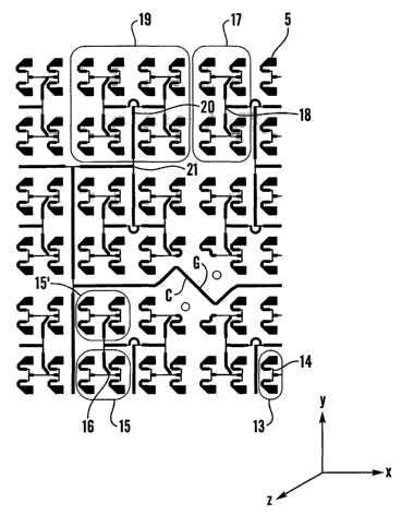
Figure 5 illustrates the first conductive path layer 4, which is arranged for
receiving
vertically polarised signals. Layer 4 comprises conductive receiving antenna
elements 5, which are connected in pairs 13 to a pair collector point 14, the
pairs 13
are connected into sub-arrays 15 to a sub-array collector point 16, the sub-
arrays 15
are connected into arrays 17 to an array collector point 18, and the arrays
are
connected into groups 19 to a group collector point 20. Two groups 19 are
connected to each other at a two-group collector point 21 and so on.
The second conductive path layer 7 has a similar structure containing
elements,
pairs, sub-arrays, arrays and groups.
The elements 5 and the sub-arrays 15 are interconnected by means of conductive
paths, and it has been shown to be particularly advantageous with regard to
loss due
to impedance mismatch to arrange the paths as illustrated in the figure, viz.
with
straight segments along a first or a second direction x or y between the
elements 5
CA 02478647 2004-09-03
WO 03/075406 PCT/N002/00092
8
and with bent segments or compensation leads between the 8-element arrays. In
the
shown embodiment the conductive paths between groups 19 comprise only
segments along the first and the second direction.
The antenna A according to the invention comprises in an embodiment four-
element
sub-arrays 15 and four columns and four rows of interconnected sub-ariays 15,
containing four groups 19 of four sub-arrays 15 as shown in Figure 5. The
number
of elements in the sub-array 15 ns and number of groups 19 ng can be selected
to
suit the applications. Similarly, the number of columns (n~) and the number of
rows
(nr) containing the groups can also be varied to suit the application. The
shape of
each conductive element (5, 8) is selected to match the polarisation, being
vertically
and horizontally oriented for vertical and horizontal polarisation
respectively. In the
embodiment described with reference to figures 4 and 5 the characteristic
numbers
are as follows:
Number of elements in the sub-array (ns) 4
Number of groups (ng) 4
Number of columns (n~) 4
Number of rows (11r) 4
Number of elements (ne) 16 x 16 - 4 = 252
The art of coupling the conductive elements (5, 8) in the sub-array 15 and the
sub-
arrays 15 in the group 19 and placing the groups 19 in the rows and columns is
based on partly established antenna theory for achieving constructive
interference to
get maximum signal at the receiving point in the middle of the complete
antenna
configuration as shown in Figure 4, in which the antenna coupling to the
receiver
LNB (Low Noise Bloclf Converter) is achieved via a field coupling mechanism
placed optimally in the vicinity of the gap between the striplines, and on a
plethora
of series of trials and errors in construction, tests and modifications that
led to the
present state of the antenna according to the invention.
The explanations given as theoretical basis in the description of this
invention hence
serve to describe the main principle of operation.
Generally, we can write the following equations,
~e = ~cgnsh~n,. -4
CA 02478647 2004-09-03
WO 03/075406 PCT/N002/00092
9
As shown in figure 5, the distance between elements in the sub-array de and
the
distance between sub-arrays ds the distance between groups dg are all selected
to
enhance the level of constructive interference needed for the optimal
performance
of the antenna in the frequency range 10.75 GHz - 12.75 GHz.
A closer loolc into the design of the antenna as shown in Figure 4 shows very
important variations of otherwise very linear streamlined patterns of the
elements 5,
8, sub-arrays 15, groups 19, columns (C ) and rows (R ). The connection
between
the sub-arrays 15 is achieved using conductive paths or striplines of suitable
length
with one segment along a third direction pointing downwards (towards -y) to
the
horizontal for both the layers of antemla meant for reception of vertically
(4) and
horizontally (7) polarised transmissions. The connection between the pair of
sub-
arrays 15 in a group 19 is achieved by using curved or bent segments or
striplines
facilitating the right phase of the signals from the pair of sub-arrays 15 in
a group
19.
The inclination angle with respect to the transmitting satellite S (figure 1)
being
depicted by cp, we find both from measurements and theory, that the distance
between rows dr is equal to the distance between the groups dg and is given by
d,.=dg=d
d= a
sin ep
Figure 6 illustrates bent or curved segments in different embodiments. As
shown in
the figure, the object of the bent or curved segments is to provide a
conductive path
that does not follow a straight line, and the shown geometries are
advantageous for
impedance compensation.
Both conductive element layers 4 and 7 are provided with collector elements.
In an
embodiment of the invention (figure 5) the collector elements C have a gap G
out of
which the total signal from all the elements in the layer will emerge. The
signal will
be received by a receiving head with an input for each layer (not shown in the
figures), which preferably has a point facing the gap G. It is also possible
to directly
connect the receiving head, LNB (Low Noise Bloclc Converter) to the antenna by
a
soldered connection. This will then replace the point and the gap but will not
come
into the same position, but will come in the middle of the path.
The receiver elements 5, 8 in the conductive element layers 4, 7 may have
different
shapes, and may be square, round, star-shaped, triangular, etc. In a preferred
embodiment of the invention the elements are in the form of oblong squares.
CA 02478647 2004-09-03
WO 03/075406 PCT/N002/00092
The plate 10 is the earth plane used in any microstripline construction. As
mentioned earlier, the horizontally and vertically polarised signals are
picked up by
a suitable set of LNBs When the two films with conductive elements are placed
directly above each other as explained, the two gap apertures will be slightly
5 displaced relative to each other. The choice of vertically or horizontally
polarised
signal is made with the help of LNBs and a suitable signal receiver (tuner).
With reference now to figure 7, an additional feature in the antenna A
according to
the invention is the incorporation of the reflector element R perpendicular to
the
plane of the antenna with a height h easily adjustable to suit the inclination
angle cp.
10 In selected applications, to enhance the received signal, the reflector R
may
incorporate perforations P (figure 8), to facilitate transmission of the
incoming
waves from the satellite S reaching the elements (5, 8) without being bloclced
by the
reflectors R. It is plausible to assume that the perforations function as new
sources
of waves just as in Huygen's wave theory. The principle of operation can be
explained as follows.
The reflectors enhance the signal quality considerably. The perforations in
the
reflectors, help wave transmission to all elements, when the antenna is
positioned at
angle ep to the vertical as shown in Figures 7 and 8. The reflector surfaces,
act as
additional sources, the phase of which has to be harmonised with the direct
signals
falling onto the elements of the patches. The maximum path covered by the
reflected wave is h cosec cp, the patch should be placed within a distance of
h cot cp.
The wave leaving the reflector after reflection will be reaching the patch
area after a
maximum delay of hlc sin cp. For the bandwidth of operation of the antenna,
these
values have to be taken into account in selecting the size of the patch and
that of the
reflector.
The receiving quality of the antenna with the plane of the antenna in vertical
position is possible with the connecting lines as shown in Figures 4 and 6.
The
reflector is not necessary for the operation of the antenna with its plane
positioned
vertically, but enhances the received signal level.
Figures 9 and 10 show different embodiments of the reflectors formed as single
reflectors (figure 9) or grouped in a strip (figure 10).
Figure 11 shows possible geometries for reflector perforations.
As stated before, the antenna according to the invention provides a simple
answer to
a long felt need by providing an easy to manufacture device which can be
mounted
on a vertical wall and tuned by an unskilled person.