Note: Descriptions are shown in the official language in which they were submitted.
CA 02479173 2004-09-13
WO 03/079558 PCT/US03/07597
A DEVICE FOR COUPLING RADIO FREQUENCY ENERGY
FROM VARIOUS TRANSMISSION LINES USING
VARIABLE IMPEDANCE TRANSMISSION LINES
CROSS-REFERENCE TO RELATED APPLICATION
This application is a continuation-in-part of US Patent No. 09/563,328, filed
May 3,
2000, which claims the benefit of U.S. Provisional Patent Application No.
60/169,722, filed
December 8, 1999.
FIELD OF THE INVENTION
The present invention relates in general to radio frequency devices and in
particular to
methods and devices for coupling radio frequency energy from transmission
lines.
DESCRIPTION OF THE RELATED ART
Until this invention, coaxial taps and couplers were installed by cutting and
connectorizing RF cable using coaxial jumpers. The primary disadvantage of
this methodology
is the resulting excessive loss to the host cable. Stein et al , U.S. Patent
5,729,184,
subsequently taught that a tap can be used without connectorization; however,
the Stein et al.
invention still caused losses of over 1 dB to the host cable. Stein et al did
mention the
theoretical ability to devise taps with coupling losses up to 20 dB but did
not describe a
method for the manufacture of such devices.
What is needed are methods and devices embodying the ability to select the
coupling
loss and accompanying insertion loss in RF systems. In particular, such
methods and devices
should allow a wireless system not only to be tuned but should also allow
minimization of the
number of amplifiers and active devices required to RF illuminate a structure.
SUMMARY OF THE INVENTION
The present invention relates generally to a coupling device for obtaining
energy from
a transmission line. In one embodiment, the coupling device comprises a
contact for
contacting an inner conductor of the transmission line through an aperture in
an outer
conductor of the transmission line. At least a portion of the contact includes
a coil of a
preselected configuration, where the configuration defines at least one
property of the
transferred energy. The coupling device also includes a connector having an
inner conductor
coupled to the contact.
In another embodiment, the coupling device includes a wire of a preselected
configuration positioned between the contact and the connector. The wire is
spaced from a
1
CA 02479173 2004-09-13
WO 03/079558 PCT/US03/07597
ground plane to create a selected parasitic capacitance and the configuration
of the wire at
least partially defines a center frequency of the coupling device.
BRIEF DESCRIPTION OF THE DRAWINGS
For a more complete understanding of the present invention, and the advantages
thereof, reference is now made to the following descriptions taken in
conjunction with the
accompanying drawings, in which:
Fig. 1 A is a schematic of a coupling device according to the principles of
the invention;
Fig. 1 B is a schematic diagram of a second coupling device according to the
principles
of the invention;
Fig. 1 C is a schematic diagram of a third coupling device according to the
principles of
the invention;
Fig. 1 D is a schematic diagram of a fourth coupling device according to the
principles
of the invention;
Fig. 2 shows an assembly and section view of the coupling device according to
the
principles of the invention;
Fig. 3A shows an electronic assembly of an ultra low insertion loss, high
coupling loss
coupling device such as that shown schematically in Fig. 1 B;
Fig. 3B shows an electronic assembly of a low insertion loss, medium coupling
loss
coupling device such as that shown schematically in Fig. 1 B;
Fig. 3C shows an electronic assembly of a low insertion loss, low coupling
loss
coupling device such as that shown schematically in Fig. 1 C;
Fig. 3D shows an electronic assembly of a low insertion loss, high frequency
coupling
device such as that shown schematically in Fig. 1A;
Figs. 4A and 4B illustrate a cutaway side view and a top view, respectively,
of a fifth
coupling device;
Figs. 5A and 5B illustrate a cutaway side view and a top view, respectively,
of a sixth
coupling device;
Figs. 6A and 6B illustrate a cutaway side view and a top view, respectively,
of a
seventh coupling device;
Figs. 7A-7C illustrate a cutaway side view, a top view, and a close up view,
respectively, of an eighth coupling device; and
Fig. 8 illustrates an alternative embodiment of the coupling device of Figs.
7A-7C.
Fig. 9 is a graph illustrating two representative samples of insertion loss
using
variations of the coupling device of Fig. 8.
2
CA 02479173 2004-09-13
WO 03/079558 PCT/US03/07597
Fig. 10 is a graph illustrating two representative samples of coupling
responses using
variations of the coupling device of Fig. 8.
Figs. 11 a-c illustrate a cutaway unassembled side view, an assembled side
view, and
a top view, respectively, of a ninth coupling device.
DESCRIPTION OF THE PREFERRED EMBODIMENTS
The principles of the present invention and their advantages are best
understood by
referring to the illustrated embodiment depicted in Figs. 1-3 of the drawings,
in which like
numbers designate like parts.
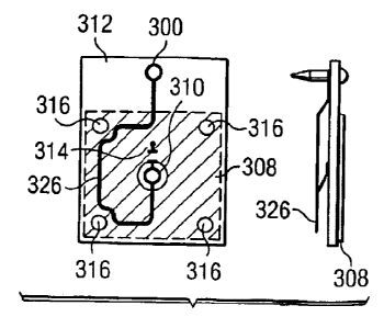
Figs. 1A and 3D respectively show a schematic and layout of a coupling device
for
coupling RF energy from a coaxial cable to a second coaxial cable, RF radiator
or RF
amplifier. Although a coaxial cable is represented, it is understood that any
transmission line
can be substituted and tapped. A hole is drilled into the host transmission
line outer conductor
100 and a contact 104 (shown in Fig. 3D at 300) is inserted to make contact
with the host
transmission line center conductor 102. The contact might be spring loaded,
but it is
understood that any means of contacting the center conductor will suffice. It
is preferable that
the center conductor contact 104 (300) be insulated, but it is not necessary
to meet the
principles of the invention. Insulation on the shaft of the contact 104 (300)
is provided to
prevent inadvertent contact with the outer conductor 100.
The coupler internal transmission line 106 (shown in Fig. 3D at 326) is a low
loss wire.
The length and diameter of the wire determine the frequency response and to
some degree,
the coupling loss and insertion loss of the device. The transmission line wire
may be insulated
to allow longer length for lower frequencies and still meet the intent of the
invention.
One principle of the invention is the use of highly conductive wire. This
prevents
dielectric loss through insulation.
The wire is connected to the center conductor pin 111 (310) of an output
connector
represented by outer conductor 110 and center conductor 111 (310). It is
understood that the
output may be a hard-wired cable, a directly connected antenna, amplifier or a
dummy load.
Any of these will meet the principles of the invention.
Loss element 112 (314) is connected between the center pin 111 (310) of the
output
connector and the outer shield 110 to provide a closer impedance match to the
device
connected to the output connector. The loss element adds to the performance of
the
invention, but is not required to meet the principles of the invention.
The configuration of Figs. 1A and 3D are used for coupling devices with
coupling
values from near-15 dB to -6 dB. The loss element of the internal transmission
line 106 (306)
is a low loss, wire. The length and diameter of the wire determine the
frequency response
3
CA 02479173 2004-09-13
WO 03/079558 PCT/US03/07597
and to some degree, the coupling loss and insertion loss of the device. The
transmission line
wire may be insulated to allow longer length for lower frequencies and still
meet the intent of
the invention. Figs. 1 B, 3A and 3B are respectively schematic and layout
diagrams of an
alternate coupling device for coupling a minimum amount of RF energy from a
host cable to
an output connector while minimizing the insertion loss in the host cable in
accordance with
the principles of the invention.
A hole is drilled into the host transmission line outer conductor 100 and a
contact 104
(300) is inserted to make contact with the host transmission line center
conductor 102. The
contact might be spring loaded, but it is understood that any means of
contacting the center
conductor will suffice. It is preferable that the center conductor contact 102
be insulated, but it
is not necessary to meet the principles of the invention.
The internal transmission line 114 (306 and 320 in Figs. 3A and 3B) is a low
loss, non-
insulated wire but may be insulated for longer lengths to accommodate lower
frequencies and
still meet the principles of the invention. The transmission line wire is not
to be in contact with
any dielectric except where it is connected to the terminal points.
The configuration of Figs. 1A and 3D are used for coupling devices with
coupling
values from near -15 dB to -6 dB. The loss element of the internal
transmission line 106
(326) is a low loss wire. The length and diameter of the wire determine the
frequency
response and to some degree, the coupling loss and insertion loss of the
device. The
parasitic capacitors 105 are formed by the diameter of the wire and the
distance from a
ground plane 108 (308) (202, Fig. 2) shown in Fig. 3D. The parasitic
capacitance and the
configuration of the wire determine the center frequency response of the
device. The
transmission line wire may be insulated to allow longer length for lower
frequencies and still
meet the intent of the invention. As shown in Fig. 3D, the PC board 312
includes holes 316
for purposes that will be described
One principle of the invention is the use of highly conductive wire. This
prevents
dielectric loss through insulation. Still another principle of the invention
is to prevent the
transmission line wire from contacting any dielectric surface except at the
point of connection.
The wire is connected to the center conductor pin 111 (310) of an output
connector
represented by outer conductor 110 and center conductor 911 (310). It is
understood that the
output may be a hard-wired cable, a directly connected antenna, amplifier or a
dummy load.
Any of these will meet the principles of the invention.
A further principle of the invention is to not connect the transmission line
to the center
contact 102 (300), but using capacitive coupling, sample the field around pin
102 as shown in
detail in Figs. 3A and 3B at 302 and 318. The greater the sampling, the
greater the coupling
energy.
4
CA 02479173 2004-09-13
WO 03/079558 PCT/US03/07597
In Fig. 1 B, an element 132 represents a complex impedance , do blocked
connection
between the transmission line 114 and the pin 104 connecting the center
conductor 102 of the
host cable. This connection is further shown in Figs. 3A and 3B. As seen in
Fig. 3A, the
connection can be small allowing a small amount of power to be coupled (from
20 to 30 dB) or
larger per Fig. 3B allowing coupling values of from 15 to 20 dB. The high
coupling loss
causes insertion losses from 0.3 to 0.05 dB.
The configuration of Figs. 1 C and 3C allows a coupling device to pass several
selected frequencies with accompanying low insertion loss at those
frequencies. In Fig. 1 C
the internal transmission line is shown at 116 and in Fig. 3C at 322. The
lumped impedance
117 on Fig. 1 C and the coil 325 shown in Fig. 3C allows the coupling device
to be configured
to emphasize selected frequencies while minimizing the insertion loss at
selected frequencies.
A further principal of this invention is that using the lumped impedance
input, such as
shown in Figs. 1 C and 3C and the selected coupling of Figs. 1 B and 3A and
3B, allows the
designer to not only select the coupling, insertion loss, but also allows him
or her to select the
required frequencies so that several frequencies can be sent and received on
the same cable.
Fig. 1 D generally relates to this invention with a do blocked, complex
impedance 119
at the input of the coupled port. This allows the designer to configure the
coupling device to
customize the return loss and to some extent the frequency response. Here, the
transmission
line (internal) is shown at 118.
Fig. 3D generally relates to the invention for coupling devices used for
single
frequencies at frequencies around 2 GHz. The principals requiring different
wire sizes to
select the coupling loss and insertion loss apply to this device as for the
other devices
described herein. It is understood that any combination of the principals of
this invention are
included as part of this invention.
Fig. 2 generally relates to the mechanical aspects of the invention. The
package
consists of 3 plastic parts, the bottom 210, the top 206 and the top seal 214.
The coupled port
connector 200 is shown as a type "N", but any applicable RF connector can be
used. The
connection to the coupled port may also be a "clamp-on" or "hard-wired". The
connection to
the host cable is 208, but it is understood that any probe or other means of
contacting the host
center conductor will meet the principals of the invention.
Captive screws 212 are used to connect the top and bottom of the device to the
host
cable. Captive screws are used to facilitate installation.
Screws 216 are disposed on opposite corners of the connector flange extending
through
holes 316 in PC board 312 (204, FIG. 2), and act as anti-rotation as well as
providing a
ground path from the host cable to the outer conductor of the coupled port.
Although the anti-
rotation is not required to allow the device to function, it adds to the
overall strength. The
5
CA 02479173 2004-09-13
WO 03/079558 PCT/US03/07597
ground is not required for operations above 400 mHz, but does add to the
overall electrical
stability. The screws 216 will generally be partially installed at the time of
manufacture and will
be finally installed at the time of installation.
Referring now generally to Figs. 4-9, further embodiments are illustrated and
will be
discussed in greater detail.
Referring now to Figs. 4A and 4B, in one embodiment, a coupling device 400
utilizes a
wire-wound coil 402 (e.g., a spring) to contact a center conductor of a
coaxial cable (not
shown). The coupling device 400 may include a housing comprising a plastic or
non-
ferromagnetic material, but the housing is not shown for purposes of clarity.
The spring 402
may comprise a non-ferromagnetic material of constant or variable pitch. In
the present
example, the spring 402 includes a coiled portion 412, a relatively straight
extension 414 at
the top of the coiled portion 412, and a relatively straight extension 416 at
the bottom of the
coiled portion 412. The wire diameter, coil diameter, and number of turns of
the spring 402
may be selected based on desired results such as coupling and insertion loss.
The bottom extension 416 of the spring 402 is connected through a secondary
transmission line 404 to a center conductor pin 406. A printed circuit board
(PCB) 408 may be
used to provide a mounting surface for the spring 402, secondary transmission
line 404, and
center conductor pin 408. In the present example, an RF interface connector
410 is mounted
on the side opposite the spring 402 and is connected to the spring 402 through
the center
conductor pin 408 and secondary transmission line 404. One or more apertures
(not shown)
in the PCB 408 may provide signal connection pathways between the two sides of
the PCB
408, as well as mounting holes.
In operation, the spring 402 may transform an impedance level from a
characteristic
transmission line impedance (e.g., approximately fifty or seventy-five ohms)
of the coaxial
cable to a higher desired value. The transformation is accomplished primarily
in the imaginary
plane and the complex impedance of the spring 402 establishes the overall
frequency
response and the amount of energy extracted from the coaxial cable. More
specifically, the
transformation is in the imaginary plane because the complex impedance is
mostly series
inductance with parasitic, turn-to-turn, capacitance. Accordingly, there is
generally little or no
resistive, real plane, component to the impedance.
The ratio of the magnitude of the complex impedance to the transmission line
impedance governs the amount of energy extracted from the transmission line.
This complex
impedance is, in part, a function of the diameter, pitch, number of turns, and
wire size of the
spring 402. In addition, the top and bottom extensions 414, 416 of the spring
402 enable a
second order control of the total complex impedance. Furthermore, the
secondary
transmission line 404 may be used to complete the complex impedance
transformation to
6
CA 02479173 2004-09-13
WO 03/079558 PCT/US03/07597
achieve the desired value. For example, the secondary transmission line 404
may control the
frequency response and the power extracted from/inserted to the coax cable.
Referring now to Figs. 5A and 5B, in another embodiment, a coupling device 500
includes a coil 502, a secondary transmission line 504, a center conductor pin
506, a PCB
508, and an RF interface connector 510 that are connected in a similar manner
to that
described in reference to Figs. 4A and 4B. In the present example, the
secondary
transmission line 504 may be provided in any configuration that allows the
desired complex
impedance over the required frequency band or bands. For example, while the
coil 502
serves as the primary impedance transformer, the secondary transmission line
504 can be a
transmission line or any passive component (such as a lumped element resistor,
capacitor, or
inductor) that may be used to achieve a desired insertion and coupling loss.
Referring now to Figs. 6A and 6B, in yet another embodiment, a coupling device
600
includes a coil 602, which may be similar to the coils 402 and 502 described
in reference to
Figs. 4 and 5, respectively. The coil 602 may comprise a single non-
ferromagnetic coil of
fixed or variable pitch and may have a fixed or variable diameter. The coil
602 is attached
directly to a center pin 604 of an RF interface connector 606. As previously
described, the
insertion loss and coupling loss of the coupling device 600 may be determined
by the wire
size, coil diameter, number of turns, and pitch design of the coil 602.
The present example may be constructed without the use of a PCB. This may
simplify
the manufacture of the coupling device 600, reduce costs, and provide similar
benefits. In
addition, the direct connection of the coil 602 to the RF interface connector
606 may prevent
energy losses that may occur if the connection is routed through a PCB.
Furthermore, the
frequency response enabled by the coil 602 may be broadband. The broadband
frequency
response may occur partly because the direct connection approach described
above removes
the circuit board and precludes the use of a secondary coil/transmission line,
which reduces
the total secondary/parasitic impedance. This reduction allows the self
resonance of the coil
602 to be moved up in frequency (out of the band of interest), resulting in a
broadband
frequency response.
Referring now to Figs 7A-7C, in still another embodiment, a coupling device
700
includes a coil 702 that is attached directly to a center pin 704 of an RF
interface connector
706. A portion of the coil 702 may be encapsulated in a material 708, such as
a low-loss
plastic (e.g., polystyrene). In the present example, the majority of the upper
portion of the coil
702 is encapsulated, while a smaller portion near the bottom is not.
The upper portion of the coil 702 acts as the principal impedance transformer
and its
complex impedance may be held invariant by mechanically constraining the
dimensions of the
coil with the material 708. The lower portion of the spring 702 acts as a
secondary impedance
7
CA 02479173 2004-09-13
WO 03/079558 PCT/US03/07597
transformer but is allowed to compress, as it is the portion of the coil 702
that maintains
contact with the center conductor of the host cable. Referring specifically to
Fig. 7C, for
purposes of illustration, the coil 702 comprises fourteen turns of American
Wire Gauge (AWG)
25 wire with an outer diameter of 0.120 inches. The portion of the coil 702
denoted by the
reference numeral "A" represents the upper 12.5 turns and is encapsulated by
the material
708. The portion of the coil 702 denoted by the reference numeral "B"
represents the lower
1.5 turns and is not encapsulated.
This encapsulating feature enables control over the coil 702 while allowing
the
coupling device 700 to be mounted on coaxial cables with varying dielectric
jacket thickness
(e.g., the unencapsulated portion can compress or expand to engage a cable).
Furthermore,
the frequency response enabled by the coil 702 may be broadband. The broadband
frequency response may occur partly because the direct connection approach
described
above removes the circuit board and precludes the use of a secondary
coil/transmission line,
which reduces the total secondary/parasitic impedance. This reduction allows
the self
resonance of the coil 702 to be moved up in frequency (out of the band of
interest), resulting
in a broadband frequency response.
Referring now to Fig. 8, in still another embodiment, the coupling device 700
of Figs.
7A-7C includes a tubular extension 710 that may extend from the device 700
into the coaxial
cable. The extension 710 may be formed as a part of the coupling device 700 or
may be
added as a separate component. The extension 710 may serve a variety of
functions such as
acting as a stabilizer for the coil 702 and as an anti-rotation device.
In addition, a cavity 712 may be provided in the housing 714 of the coupling
device
700. The cavity 712 may be sized to adjust the parasitic capacitance, which
serves to fine-
tune the frequency response. More specifically, the cavity 712 may form an
electromagnetic
resonant circuit. When the coil 702 (or a transmission line) is introduced
inside the cavity 712,
the fields surrounding the coil 702 are constrained (e.g., there are
electromagnetic boundary
conditions that may not exist in an unconstrained space). Accordingly, the
cavity 702 will
exhibit a largely imaginary complex impedance, which may be capacitive.
Referring now to Fig. 9, a representative insertion loss from a tap is
illustrated by a
graph 900. The graph 900 includes an x-axis 902 representing frequency in MHz
and a y-axis
904 representing insertion loss in dB. Two samples 906 and 908 each represent
an
exemplary behavior pattern of two different variations of the coupling device
700 of Fig. 8.
The exemplary behavior of the sample 906 illustrates a result when a nominal
amount of
power is being extracted, while the sample 908 illustrates a result when the
amount of power
being extracted is increased by approximately 3 dB.
8
CA 02479173 2004-09-13
WO 03/079558 PCT/US03/07597
Referring now to Fig. 10, a representative coupling response from a tap is
illustrated
by a graph 1000. The graph 1000 includes an x-axis 1002 representing frequency
in MHz and
a y-axis 1004 representing coupling loss in dB. Two samples 1006 and 1008 each
represent
an exemplary behavior pattern of two different variations of the coupling
device 700 of Fig. 8.
The exemplary behavior of the sample 1006 illustrates a result when a nominal
amount of
power is being extracted, while the sample 1008 illustrates a result when the
amount of power
being extracted is increased by approximately 3 dB.
The samples 906, 908 and 1006, 1008 in the graphs of Figs. 9 and 10,
respectively,
are based on two variations of Fig. 8. The samples 906 and 1006 are the
corresponding
results from a single variation, and the samples 908 and 1008 result from an
additional
variation. For example, the variation represented by the samples 906 and 1006
may be
created with a baseline coil length, coil inner diameter, coil wire size, and
coil number of turns.
Having established this baseline, the samples 908 and 1008 may result when a
variation is
created with the same coil length but 20 percent reduction in coil turns, 10
percent increase in
coil diameter, and a 5 percent increase in coil wire size. Both variations are
based on
constant diameter and constant pitch coils. Similar results can be achieved by
utilization of
one or both of these parameters instead of, or in combination with, the
parameters that were
varied. Furthermore, it is understood that a variety of parameters may be
utilized to produce a
desired variation.
Referring now to Figs. 11a-c, in still another embodiment, an exemplary
coupling
device 1100 includes a coil 1102, a secondary transmission line 1104, a center
conductor pin
1106, a PCB 1108, and an RF interface connector 1110 that are connected in a
similar
manner to that described in reference to Figs. 4 and 5. As described
previously, the
secondary transmission line 1104 may be provided in any configuration that
allows the desired
complex impedance over the required frequency band or bands. For example,
while the coil
1102 serves as the primary impedance transformer, the secondary transmission
line 1104 can
be a transmission line or any passive component (such as a lumped element
resistor,
capacitor, or inductor) that may be used to achieve a desired insertion and
coupling loss.
The device 1100 includes a housing 1112. In the present example, the housing
1112
comprises a lower housing 1112a, an upper housing 1112b, and a top plate
1112c. The top
plate 1112c may be fastened to the upper housing 1112b by a plurality of
screws 1114 and
the upper housing 1112b may be fastened to the lower housing 1112a by a
plurality of screws
1116. Other fastening means may be used to replace or complement the screws
1114 and
1116.
The device 1100 may also include a tubular extension 1118 and a cavity 1120 as
described in reference to Fig. 8. The tubular extension 1118 may extend from
the device
9
CA 02479173 2004-09-13
WO 03/079558 PCT/US03/07597
1100 into the coaxial cable. The extension 1118 may be formed as a part of the
coupling
device 1118 or may be added as a separate component. The extension 1118 may
serve a
variety of functions such as acting as a stabilizer for the coil 1102 and as
an anti-rotation
device. The cavity 1120 may be provided in the housing 1112 of the coupling
device 1100.
For example, the cavity may be formed in the upper housing 1112b as
illustrated. The cavity
1120 may be sized to adjust the parasitic capacitance, which serves to fine-
tune the frequency
response as previously described.
Although the invention has been described with reference to a specific
embodiments,
these descriptions are not meant to be construed in a limiting sense. Various
modifications of
the disclosed embodiments, as well as alternative embodiments of the invention
will become
apparent to persons skilled in the art upon reference to the description of
the invention. It
should be appreciated by those skilled in the art that the conception and the
specific
embodiment disclosed may be readily utilized as a basis for modifying or
designing other
structures for carrying out the same purposes of the present invention. It
should also be
realized by those skilled in the art that such equivalent constructions do not
depart from the
spirit and scope of the invention as set forth in the appended claims. It is
therefore,
contemplated that the claims will cover any such modifications or embodiments
that fall within
the true scope of the invention.