Note: Descriptions are shown in the official language in which they were submitted.
CA 02479334 2010-07-19
HIGH SPEED ANALYZER USING NEAR INFRARED RADIATION
TRANSMITTED
THROUGH THICK SAMPLES OF OPTICALLY DENSE MATERIAL
Field of the Invention
The present invention relates to means for measuring in relatively short
periods of time
constituents in optically dense materials using medium resolution spectra in
the near infrared range
transmitted through thick samples of the material while the material is either
stationary or flowing.
More particularly, though not exclusively, the present invention relates to a
method and apparatus
using a specific type of near infrared spectrometer developed for this purpose
in combination with a
spectral based model to measure percentages of the major constituents of
stationary or flowing
material such as grains, processed foods, pharmaceuticals, chemicals, and
other industrial or
agricultural products.
Background of the Invention
The measurement of near infrared (NIR) spectra is over 200 years old and
research into NIR
analyzers began over 50 years ago. "The foundations for modern NIR analysis
began to be laid in
the 1950's when the USDA had embarked on a programme of research aimed at
developing
chemico-physical methods for rapidly assessing the quality of agricultural
commodities." (Osborne
et al., 1993, p 3).
NIR Analyzers have been used for over 30 years to measure constituents of
grain, fruit, milk,
and meat. After initial applications in the agricultural area, instruments
with industrial applications
22006448.1
CA 02479334 2004-09-15
WO 03/081188 PCT/US03/08417
were developed. NIR analyzers for pharmaceuticals, refining, chemical
manufacturing, and medical
diagnostics emerged.
The function of NIR quantitative analyzers is to predict or estimate the
concentrations of
various constituents in a substance using the NIR spectra of energy that has
passed through at least a
portion of that substance. All NIR analyzers perform the same basic
operations:
1. Generate energy in some portion of the NIR band (roughly 700 to 2500 nm);
2. Either temporally, spatially, or in combination separate the NIR energy
into narrow
adjacent bands;
3. Apply energy to the substance under test;
4. Collect a portion of the energy that has passed through part or all of the
substance;
5. Measure and record the intensity of the collected energy in one or more of
the narrow
bands using a suitable detector; and
6. Apply the spectral magnitudes at selected wavelengths as inputs to models
developed to
predict concentrations of different constituents.
The second, third, and fourth operations are not necessarily performed in the
sequence
listed. For example, if the energy is spectrally separated in time only or
both in time and space, this
is typically done before the narrow band energy is applied to the substance.
If instead the energy is
only separated spatially, this operation is typically performed on the
collected portion of the energy
that has passed through the substance.
There are a number of different devices or techniques that can be used to
accomplish each
of the six main operations of an NIR analyzer:
1. NIR Energy Generation:
Tungsten Halogen Lamp
Light Emitting Diode (LED)
2
CA 02479334 2004-09-15
WO 03/081188 PCT/US03/08417
2. Spectral Separation:
Scanning or oscillating diffraction grating
Fixed diffraction grating
Rotating narrow band filter
Rotating variable filter
Fourier Transform (FT) Interferometer
Acousto-Optical Tunable Filter (AOTF)
3. NIR Energy Delivery to Substance
Collimating Optics - Direct Output
Collimating Optics with Intervening Fiber Optics
4. NIR Energy Collection From Substance
Reflected Energy Focusing Optics - Direct Output
Reflected Energy Focusing Optics with Intervening Fiber Optics
Transmitted Energy Focusing Optics - Direct Output
Transmitted Energy Focusing Optics with Intervening Fiber Optics
5. Measurement of Collected NIR Energy.
Single Detector
Detector Array (DA) with Serial Output
The detector type used depends on the wavelength range of the analyzer. Common
detector types are:
Photomultiplier
Silicon Photodiode
InGaAs photodiode
PbS photoresistor
3
CA 02479334 2004-09-15
WO 03/081188 PCT/US03/08417
6. Prediction of Constituent Concentration:
Chemometric Models: MLR, PLS, PCA
Neural Net Models
Genetic Algorithms
Combinations of these
The energy collected can be broadly categorized as belonging to one of two
main types:
diffuse reflectance spectra and transmitted spectra. For diffuse reflectance
analyzers, the delivery
optics and the collection optics are placed on the same side of the substance
so that the collection
optics receives near infrared radiation reflected diffusely off of the
substance being measured. For
transmittance analyzers, the delivery optics and collection optics are placed
on opposite sides of the
substance so that the collection optics receives radiation that has been
transmitted through the
substance being measured.
Commercial NIR analyzers first appeared in the 1970's in the food and
agriculture industry
(Osborne et al., 1993, pg. 3). The analyzers were designed to measure various
constituents of food
such as protein, oil, and starch. For the first decade, all commercial
instruments were filter based
(Osborne et al., 1993, pg. 5). Filter instruments continued to dominate into
the middle of the 1980's:
"The two main methods by which most commercial near-infrared instruments
generate
wavelengths are the discrete filter and the tilting filter principles."
(Williams and Norris,
1987, pg. 113)
Although filter instruments dominated for the first 10 to 15 years in
commercial instruments
there was another wavelength separation technique that found early favor in
research analyzers and
on which some commercial units were based. That technique was the scanning
monochromator
(SM) using a motor driven diffraction grating (Williams and Norris, 1987, pg.
126-127; Burns and
Ciurczak, 2001, pg 61 - 65).
4
CA 02479334 2004-09-15
WO 03/081188 PCT/US03/08417
Just as filter based monochromators dominated initial commercial instruments,
reflectance
spectroscopy was also favored over transmittance. This was mainly due to the
fact that the earlier
instruments used wavelengths in the 1200 to 2500 nm range (Naes and Isaksson,
1992, pg. 34).
Diffuse reflectance analyzers have several advantages over transmittance
analyzers:
1. Many substances being measured are optically dense (opaque). Therefore, for
a given
resolution spectrometer and given source intensity, use of transmittance
spectra instead
of reflectance spectra requires use of thinner samples (short optical path
lengths), high
powered sources, and/or an integrating detector with long integration times;
and
2. The mechanical design of reflectance analyzers is sometimes simpler than
transmittance
spectrometers as both source and detector are placed on the same side of the
sample.
There are, however, disadvantages to reflectance analyzers. Some of the major
disadvantages
are:
1. Reflectance spectrometers only measure a thin layer of the surface of the
substance being
measured. This is a disadvantage if the material is not homogeneous. In
contrast,
transmittance spectrometers measure the entire body of material;
2. Reflectance spectrometers require use of a separate reference to establish
the reference
signal. An ideal reference material will diffusely reflect all incident
radiation in the
wavelength range of interest. Typically the reference material is inserted
mechanically
between the incoming radiation and the sample window when a reference reading
is
made; and
3. Reflectance analyzers are affected more than transmittance analyzers by
scattering or
dusty environments (Osborne et al., 1993, pg. 92-93). This problem is most
severe when
granular material such as grain is being measured. When a thin layer of dust
accumulates
5
CA 02479334 2004-09-15
WO 03/081188 PCT/US03/08417
on the surface of the sample chamber input window, most of the incident
radiation will
reflect off of the layer of dust and little off of the grain inside the sample
chamber. The
acquired spectrum is therefore mainly that of the dust. For transmittance, the
dust will
reduce the signal. It will also change the spectral signature of the source
incident
radiation illuminating the grain. But the accumulated dust will also change
the spectral
signature of the reference signal, which is acquired when the sample chamber
is empty.
As long as the spectral signatures of the incident radiation penetrating the
dust are closely
matched for reference and sample signals, normalization will eliminate the
dust spectra.
This will enable an accurate representation of the grain absorption spectrum
to be
calculated. For reflectance mode spectrometers placement of the reference
material
inside the sample chamber is difficult or expensive to do. It is normally
placed outside of
the sample chamber and mechanically moved in front of the sample chamber
window
when a reference signal is to be acquired. In this situation, the dust spectra
will not be
removed by normalization.
Although filter and scanning grating based analyzers dominated commercial and
research
applications initially, in recent years other techniques such as Fourier
Transform -Near Infrared (FT-
NIR) technology in industrial applications and Diode Array based analyzers
have emerged.
Transmittance analyzers have also been developed in the past 15 years for use
in medical,
pharmaceutical, and agricultural measurement and control.
In spite of the progress that has been made in the development of NIR
analyzers and their
many different uses, there are a number of deficiencies that prevent wider
application of the
technology. New markets await the development of an NIR analyzer with the
following features:
1. Low cost;
6
CA 02479334 2004-09-15
WO 03/081188 PCT/US03/08417
2. Rugged: operation in presence of dust and vibration;
3. Temperature Stability;
4. Fast Analysis: Take rapid readings even when the intensity of collected
energy is low;
5. Operate in transmittance mode analyzing relatively thick samples of
optically dense
material;
6. High Dynamic Range: Able to measure a wide range (1,000,000:1) of input
intensities
automatically; and
7. No moving parts.
An analyzer required to meet all of these criteria precludes the use of many
of the devices
and techniques used in NIR Analyzers listed above:
1. NIR Energy Generation: Tungsten Halogen Lamps are preferred
LED's in general have insufficient light output and spectral range
2. Spectral Separation: Fixed Diffraction Gratings are preferred
Scanning gratings, rotating filters, AOTF and FT-NIR are too slow
Scanning gratings, rotating filters, and FT-NIR have moving parts, and are
vibration
sensitive
Filters are not temperature stable and temperature stabilization is expensive
FT-NIR and AOTF are expensive.
3. NIR Energy Delivery to Substance: Collimating Optics is preferred
Fiber Optics reduces the intensity too much.
4. NIR Energy Collection From Substance: Collection of Transmitted Energy
through
focusing optics is preferred
7
CA 02479334 2004-09-15
WO 03/081188 PCT/US03/08417
Reflected Energy is susceptible to dust and uses moving parts to measure
energy
reflected off of reference material
Fiber Optics reduces intensity too much
5. Measurement of Collected NIR Energy. No Suitable Choice
Single Detector is too slow and requires moving parts. Wavelengths have to be
scanned
which is too slow, requires moving parts, and is subject to vibration.
Detector Array (DA) with Serial Output: is too slow as output of array has to
be scanned
serially. The elements of typical diode arrays are too small so that outputs
for low level
intensity signals are too low.
The detector type used: Silicon is preferred
Photomultipliers are too expensive
InGaAs photodiode is too expensive, insensitive and requires temperature
stabilization
PbS photoresistor is too expensive, insensitive and requires temperature
stabilization
There are no commercially available spectrometers that can be used to
construct an NIR
analyzer with the requirements specified above. The closest devices available
are the diode array
spectrometers such as the S2000 from Ocean Optics. But these suffer from a
number of drawbacks.
The diode arrays have a large number of photodiodes - from 512 to 2048. This
means that the
power incident on each photodiode is very low. On top of that, the arrays are
scanned serially (as
they must be with so many detectors). Thus low intensity signals that would
come from NIR energy
transmitted through relatively thick samples of optically dense material would
take a long time to
acquire if they could be acquired at all. In addition the dynamic range of the
instrument is limited
and would not permit acquisition of a reference signal that is 1000x greater
or more in intensity than
the sample signal. A neutral density filter would have to be mechanically
inserted when the sample
chamber is empty in order to acquire and measure the reference signal.
Finally, most of the small
8
CA 02479334 2004-09-15
WO 03/081188 PCT/US03/08417
medium priced diode array based spectrometers are designed only for fiber
optic inputs, decreasing
the signal strength even further. In summary, the diode array based
spectrometers available today
are too slow, have too little dynamic range, and do not collect enough energy
to meet the specified
requirements.
Summary of the Invention
The present invention relates to means for measuring in relatively short
periods of time
constituents in optically dense materials using the spectra of near infrared
radiation transmitted
through even relatively thick samples of the material while the material is
either stationary or flowing.
The invention uses a broadband incandescent intensity controlled light source
combined with
collimating optics to transmit a parallel beam of light through the material
under test. The light
transmitted through the material is then collected by a focusing lens and
imaged onto a rectangular
entrance slit of a special purpose spectrometer. This spectrometer has no
moving parts and employs
a fixed diffraction grating to physically spread the image of the entrance
slit into a continuous range
of wavelengths. A portion of that diffracted slit image covering a portion of
the near infrared range
is imaged onto an array of individual rectangular photodiodes. The slit
dimensions are the same as
the individual photodiode dimensions. The slit and photodiodes are oriented in
the same direction
with the long side of the slit parallel to the long sides of the individual
photodiodes. By using arrays
with a relatively small number of large active area photodiodes, high
sensitivity is achieved and low
intensity radiation levels can be measured quickly. By using a relatively
narrow spectral range,
medium resolution can be achieved. The outputs of each photodiode, or the
outputs of a selected
number of the photodiodes are fed into current to voltage converters: either
resistive (instantaneous)
or the preferred capacitive (integrating). Thus the outputs of all photodiodes
are measured in
parallel. This parallel operation also reduces the time to acquire the
spectra. After the spectra are
9
CA 02479334 2004-09-15
WO 03/081188 PCT/US03/08417
acquired, they are operated on by models developed to predict the percentages
of various
constituents in the material. These models are pre-calibrated using spectra
obtained from materials
of known concentrations and developed using chemometric, neural net, and/or
genetic algorithms.
Brief Description of the Drawings
Figure 1 is a block diagram of a NIR transmittance analyzer designed to
analyze stationary
material.
Figure 2 is a block diagram of the NIR transmittance analyzer designed to
analyze flowing
material.
Figure 3 is a diagram of a light source, entrance optics, sample chamber, and
exit optics of
the analyzer.
Figure 4a is a front view of a spectrometer of the analyzer.
Figure 4b is a side view of the spectrometer.
Figure 4c is a view of a photo diode array of the spectrometer shown from the
line A-A of
Figure 4b.
Figure 5 is a block diagram of an electronics portion of the analyzer.
Figure 6 is a front view of a slit and off axis photodiode assembly of the
spectrometer.
Detailed Description of the Invention
The following description of the present invention applies to its preferred
embodiment.
Those of ordinary skill in the art will understand that the present invention,
however, is not limited
to the described embodiment.
CA 02479334 2010-07-19
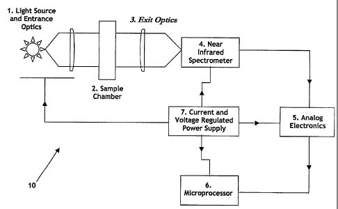
Figures 1-2 show a block diagram of the NIR analyzer 10 for use on stationary
and flowable
material respectively. Seven major components of the analyzer 10 are
identified in Figures 1-2.
These components and their functions are:
Light source and entrance optics, comprising an incandescent light source 1
that generates
a broad spectrum of radiant energy including a continuous component in the
selected near
infrared range. Part of this radiant energy is collected by a lens and
collimated into an
approximately parallel beam. This beam is transmitted through a transparent
window 17 into
the sample chamber 2 holding the material;
Sample chamber 2 is a fixed rectangular chamber for holding the material whose
constituents
are to be measured, with the transparent entrance window 17 and a transparent
exit window
19 attached to opposing sides that are transparent to visible and near
infrared radiation;
Exit optics, consisting of a diffuser 20 to further homogenize radiation from
different parts
of the sample chamber; and a focusing lens 21 to focus the radiation emerging
from the
diffuser onto an entrance slit/detector assembly 22 of a spectrometer 4;
Spectrometer 4 is a near infrared spectrometer for spreading radiation
illuminating an
entrance slit 23 in a continuous spectrum, with wavelengths covering a narrow
band
(nominally 200 nm) in the near infrared range, being imaged onto an array 26
of individual
photodiode detectors;
Analog electronics comprising a set of integrator-comparator-timer circuits to
integrate the
output current from each photodiode into a voltage level and measure the time
to reach a
fixed reference voltage;
Microprocessor 6 with associated embedded program to control the operation of
the
spectrometer 4 to acquire the integration times which are inversely
proportional to spectral
intensity incident on each photodiode (as intensity decreases, integration
time increases), and
22006448.1 11
CA 02479334 2004-09-15
WO 03/081188 PCT/US03/08417
operates on the spectral intensities with a suitable model to predict
constituent
concentrations in the illuminated material; and
Current and voltage regulated power supply to maintain constant intensity
output from the
light source 1.
All of these components combined constitute the near infrared transmittance
constituent
analyzer 10 whose general operation is detailed in the remaining 5 Figures and
is now described.
The basic operation of the analyzer 10 is to acquire magnitudes of selected
spectral bands (nominally
5 nm in width) in the selected range (nominally 200 nm) of near infrared
radiation transmitted
through an optically dense material. These spectra are then used to predict
concentrations of one of
more of the constituents of the material based on the spectral magnitudes. The
prediction is done
using pre-calibrated models for each constituent with the inputs to each model
being the spectral
magnitudes and the output being the predicted concentrations. The sequence of
events that lead to
this result are: generation of a broadband continuous spectrum light that
includes a component in
the near infrared range selected; illumination of the material under test with
a portion of that light;
collection of a portion of that light that is transmitted through the material
and focusing it on the
entrance slit 23 of the spectrometer 4; spreading of the light inside the
spectrometer 4 so that the
wavelengths in the selected range are imaged onto a photodiode array 26;
conversion of the output
of each photodiode to a spectral magnitude; operation on all spectral
magnitudes by a constituent
prediction model to predict constituent concentration in the material. The
details of this process are
now presented.
Referring to Figure 3, the light source 1 consists of an incandescent source
whose power
input is held constant by a voltage and current controlled power supply 7. An
example of a suitable
light source is a tungsten halogen lamp, with a precisely positioned element,
encased in a quartz
envelope. Ideally the element dimensions are the same as the slit and
photodiode dimensions. A
12
CA 02479334 2010-07-19
portion of the output of the lamp is collected by a collimating lens 16 and
exits the lens as a beam.
The beam is directed perpendicular to a transparent window 17 and passes
through the window into
the material contained in the sample chamber 2. Some of the light is
reflected, some scattered,
some absorbed, and some transmitted directly through the material. Some of the
transmitted and
scattered light passes through the exit window 19 out of the sample chamber.
The light emerging
from the sample chamber 2 is then further homogenized by the diffuser plate
20. A portion of the
light emerging from the diffuser plate 20 is collected by a focusing lens 21
and focused onto the
entrance slit/detector assembly 22 of the spectrometer 4.
The entrance slit/detector assembly 22 consists of an optically centered
entrance slit 23 of
rectangular shape and dimensions equal to the dimensions of the individual
rectangular photodiodes
that make up the photodiode array 26. The entrance slit dimensions are aligned
with the individual
photodiode dimensions in the sense that the long side of the slit 23 and the
individual photodiodes
are parallel and the short sides are parallel with reference to the light
beam. The assembly 22 also
consists of an off center photodiode detector 48 used to measure the relative
total intensity of the
incoming radiation and is used in the process of taking reference calibration
readings.
The light illuminating the off centered detector 48 results in a current
output which is
measured by the computer and converted to a digital value. The computer uses
the digital value to
determine whether the sample chamber 2 is empty and a reference spectrum is
being acquired or if
the sample chamber 2 is full and a sample spectrum is being acquired. The
computer then sets the
integrator clock accordingly so that the clock period is short for the
reference signal and long for
the sample signal (see below).
The light focused on the centered entrance slit 23 enters the spectrometer and
is collected by
a slit collimating mirror 25. The slit collimating mirror 25 collimates the
light passing through the
slit 23 and directs the beam toward the diffraction grating 29. The
diffraction grating 29 spreads the
22006448.1 13
CA 02479334 2004-09-15
WO 03/081188 PCT/US03/08417
collimated light into a continuum of wavelengths. This diffraction pattern is
then focused into a
continuum of slit images by a diffraction pattern focusing mirror 24 onto the
photodiode array 26.
The spectrometer 4 is designed so that the sequence of slit images of unit
magnification is focused
onto the array 26 - one image per photodiode - and each image covers a
different narrow band of
wavelengths. If the selected near infrared range is 800 nm to 1000 nm, the
slit images would start at
800 nm at one end of the array and end at 1000 nm at the other end of the
array.
The photodiode array is mounted on a printed circuit board 27 with an aluminum
plate and
optional kapton flexible heater 28 attached to the back of the printed circuit
board. The flexible
heater 28 is used to maintain the photodiode array 26 at a constant and
slightly elevated fixed
temperature so that the outputs of the diode array 26 will not vary with
changes in ambient
temperature. The heater strip 28 could be replaced with a thermoelectric
cooler instead. A third
alternative would be to eliminate the temperature control, add a temperature
sensor, and calibrate the
analyzer 10 at different temperatures. A fourth alternative would be to use no
temperature control
or monitoring at all, and only use the analyzer 10 when such control is not
required.
The output of each photodiode of the photodiode array 26 is independent so
that all outputs
can be accessed in parallel. The outputs of each photodiode are connected to
the printed circuit
board 27 of the analog electronics interface module 5. Referring to Figure 5,
on this printed circuit
board, a selected number of the photodiode outputs - Ido 31 through IdN 47 -
are connected to
integrators - Integrator 0 32 through Integrator n 46. The integrators are
controlled by the integrator
enable signals - Integrate Enabled 40 through Integrate EnableN 41 - from the
microprocessor 39.
When the integrator enable signals are off, the integrator output voltages -
VIo 33 through VI. 45 -
are held at zero volts. When the integrators are enabled, the current coming
from the individual
photo diodes of the photo diode array 26 charge the integrator charge storage
devices (capacitors)
and the integrator output voltage magnitudes increase over time at rates
proportional to the
14
CA 02479334 2004-09-15
WO 03/081188 PCT/US03/08417
photodiode currents (which are proportional to the intensity of the radiation
incident on the
photodiodes - the lower the current the lower the intensity). The integrator
output voltages are
compared with a reference voltage Vref 34 by comparators CMP, 35 through CMPn
44. When the
magnitude of an integrator output voltage reaches the reference voltage, the
output of the
corresponding comparator switches off. The output of each comparator - Gateo
36 through Garen
43 - serves as an enable input to a timer - Timer, 37 through TimerN 42. The
timers are also
controlled by the integrate enable signals so that when an integrate enable
signal is off, the integrator
output voltage is zero, the Gate signal is on, and the timer is disabled. When
an integrate enable
signal is switched on, the Gate signal remains on, and the timer is enabled.
When the timer is
enabled, it begins counting and continues counting until the corresponding
integrator voltage output
signal magnitude reaches the reference voltage level. At this time the gate
signal is switched off and
the timer stops counting.
The master clock for the timers is set depending on whether the sample chamber
2 is empty
or full. The off centered photodiode detector 48 next to the spectrometer
entrance slit 23 is used to
measure the relative total intensity of the radiation that has been collected
after passing through the
sample chamber 2. If that intensity level is sufficiently high, then the
sample chamber 2 is assumed
empty and the reference spectra are acquired. The master clock rate is set
high. If the intensity is
sufficiently low, then the sample chamber 2 is assumed to be full and sample
spectra are acquired.
The master clock rate is set low in this case.
The final count value from any timer is a measure of the time required for the
corresponding
integrator voltage to reach the reference voltage. This count is therefore
(for an up-counter)
inversely proportional to the magnitude of the photodiode current, which in
turn is proportional to
the intensity of the incident radiation on the photodiode. The final count is
inversely proportional to
the intensity of radiation over the narrow spectral band illuminating the
photodiode. Thus for a low
CA 02479334 2004-09-15
WO 03/081188 PCT/US03/08417
intensity signal, the photodiode current will be low, the integration time
long, and the count high.
For a high intensity signal, the photodiode current will be high, the
integration time short, and the
count low.
The final counts for each timer will be different because the radiant
intensities on each
photodiode will be different. The final counts will be representative of the
spectral absorption
signature in the selected near infrared range (800 to 1000 nm, for example) of
the radiation
transmitted through the material under test. Thus for a low intensity signal,
the absorption is high
and the count is high. For a high intensity signal, the absorption is low and
the count is low. The
final counts are read by the microprocessor 6 over a data bus 38 connecting
the timers to the
microprocessor 6.
After acquisition of the final counts, the microprocessor 6 operates on these
counts using
constituent prediction models to estimate the concentration of different
constituents of the material
under test. These models are pre-calibrated using materials of known
concentrations and developed
using chemometric, neural net, and/or genetic algorithms.
The analyzer 10 is designed in order to provide a low cost medium resolution
near infrared
transmittance instrument with no moving parts capable of measuring at least
relatively thick samples
of optically dense material quickly, while also capable of measuring high
intensity reference signals
without changing the intensity of the light incident on the sample chamber.
Low cost and ability to
measure low signal levels are aided by using standard quartz tungsten halogen
lamps and individually
addressable large area silicon photodiodes. High speed is accomplished by
using individually
addressable photodiodes whose outputs are converted in parallel to voltage
levels by high gain
integrators. Ability to measure a wide range of spectral intensities without
changing incident
intensity is accomplished by using counters with programmable clock rates. A
low clock frequency
is used to measure the spectral signature of light transmitted through the
sample, and a high clock
16
CA 02479334 2004-09-15
WO 03/081188 PCT/US03/08417
frequency for the spectral signature of light transmitted through an empty
sample chamber
(reference spectra). This design also eliminates the need for moving parts.
Medium resolution is
achieved by restricting the detected range to a nominal 200 nm and by the
spectrometer physical
design.
In order to design an analyzer that meets the listed specifications, a new
spectrometer must
be designed. The design must balance cost, source power, energy collection
efficiency, resolution,
and speed in order to achieve the desired performance. For this spectrometer
the first four
operations of the NIR analyzer listed in the Background of the Invention would
use the preferred
devices already identified. The fifth operation - detection - would require
use of a device not
commonly used in NIR spectrometers: a linear silicon photodiode array 26 with
parallel outputs and
a small number of large area individual photodiodes. This would be combined
with special interface
electronics to enable fast stable conversion of the individual detector output
photocurrents. The
complete spectrometer 4 in its preferred embodiment consists of
NIR energy generation consisting of a tungsten halogen lamp 1 with electronic
stabilization
to maintain constant intensity output and lamp element dimensions selected to
match as
close as possible the spectrometer input slit dimensions;
Spectral separation comprised of a fixed diffraction grating 29 designed to
spread the
collected energy over the diode array 26 in the preferred wavelength range
(800 to 1000 nm,
for example);
NIR energy delivery to substance comprising collimating optics is preferred
with direct
transfer to the sample chamber 2 and through the sample chamber window 17;
NIR energy collection from substance comprising collection of transmitted
energy through
focusing optics, with direct transfer to the input slit 23 of the spectrometer
4. The lamp
17
CA 02479334 2004-09-15
WO 03/081188 PCT/US03/08417
filament, collimating optics, and focusing optics are designed so that an
image of the filament
is focused onto the spectrometer entrance slit 4;
Measurement of collected NIR energy through use of a linear silicon photodiode
array 26 of
a limited number (less than 50) of relatively large area photodiodes. The
photodiodes in the
array 26 are individually addressable. Timer based integrators are used to
measure the
relative intensity of the narrow band radiation incident on each photodiode.
This analyzer 10 involves 5 major changes to typical commercially available
diode array
spectrometers. One of the most innovative aspects of the design is the use of
a diode array
comprised of a relatively small number of large area photodiodes (less than
50). Most commercial
diode array spectrometers use arrays with 512, 1024, or 2048 detectors. A
second related innovation
is use of a diode array with individually addressable photodiodes instead of a
serial output array. The
two innovations combined enable fast conversion of low intensity signals.
The third major innovation in the design is the use of per channel time based
integrators
with special design features to enable conversion of both low and high level
signals while meeting
the requirements of fast conversion time, high resolution, and no moving
parts. The integrators
measure the photocurrents from each photodiode, which are proportional to the
intensities of the
NIR radiation in each narrow band of wavelengths incident on the individual
photodiodes. The
timed-based integrators consist of a switched integrator, integrating
capacitor, timer, clock, voltage
reference, and comparator. With the integrator switched off the capacitor
voltage is fixed at 0 volts.
When the integrator is turned on, the timer is started and the photocurrent
from the associated
photodiode begins charging the integrator capacitor. When the capacitor
voltage reaches the voltage
reference the comparator changes state. This stops the integrator and the
timer. The final count in
the timer is a measure of the time required to charge the integrator capacitor
to the reference voltage
level and is inversely proportional to the photodiode current (low current,
high count).
18
CA 02479334 2004-09-15
WO 03/081188 PCT/US03/08417
The task of meeting the requirements of fast conversion, high resolution, and
no moving
parts while measuring both high and low level signals is made much simpler if
one or more of the
timed integrator circuit parameters is made programmable in real time. There
are three main
parameters that could be made selectable: the integrator capacitor; the timer
clock frequency; and the
comparator reference voltage. Of these three, it is not practical to switch
the capacitor in real time.
This leaves just two options: the clock and the reference voltage. The value
of the capacitor is
preferably fixed.
The value at which the capacitor is fixed depends on which of the three
requirements has
highest priority. In most applications, fast conversion time will be most
important. Therefore, in
order to convert low level photocurrents quickly, the lowest practical
capacitor value is selected.
The lowest practical value of the integrator capacitor is determined by
manufacturing
constraints (obtainable accuracy for low valued capacitors), and physical
constraints (lowest practical
level of stray capacitance). It also depends indirectly on the intensity level
of the reference spectrum,
the maximum value of the voltage reference, and the maximum clock frequency
that is practical.
With the integrator capacitance set to a low value, the high photocurrent that
occurs when
measuring the reference signal will quickly charge the capacitor. If the clock
and/or voltage
reference levels are too low, then the final count will also be low. If the
final count is too low, then
the reference signal measuring resolution will be too low. Therefore, both the
clock and the voltage
reference level are set to their maximum values to enable sufficient
resolution. The minimum
capacitance value is then equal to the value that will guarantee the minimum
acceptable measurement
resolution (unless manufacturing or physical constraints require a higher
value).
Setting the integrating capacitor, clock rate, and voltage references in this
way guarantees
satisfactory operation when reference signal measurements are made, but
compromises performance
and may create problems when measuring low level sample signals. The
performance is
19
CA 02479334 2004-09-15
WO 03/081188 PCT/US03/08417
compromised because the reference voltage level is set to its maximum value.
The purpose of this is
to slow down the time for the reference signal current to charge the capacitor
so that the final count
will be high enough to insure adequate measurement resolution. This also slows
down the time
required for the low level sample spectrum to be acquired increasing the
spectral acquisition time
and thereby degrading performance. There are other potential problems caused
by using the
maximum clock frequency and maximum reference voltage. The maximum reference
voltage
increases the acquisition time as already noted. This coupled with a high
clock frequency can result
in a large final count if the sample signal intensity is orders of magnitude
lower than the reference
signal intensity. This problem can be overcome if sufficiently wide counters
are used (24 bit or 32
bit instead of 16 bit for example). However there may be practical or cost
constraints on the
maximum width of the counter.
These two problems are resolved in this design by making both the voltage
reference level
and the clock frequency programmable. The voltage reference level is set high
when measuring high
intensity reference signals and low when measuring low intensity sample
signals. This enables high
resolution measurements for both signals and minimizes conversion time for
sample signals.
Similarly, the clock frequency is set high when measuring reference signals to
enable adequate
measurement resolution. The frequency is set low for sample signals in order
to minimize the
required counter width.
Determination of when reference signals and when sample signals are being
measured is
accomplished as follows. A separate photodiode 48 external to the spectrometer
4 is mounted near
the entrance slit 23 and measures the total intensity of the incoming
radiation. This measurement is
used to determine whether the sample chamber is full or empty and therefore
whether a sample
spectrum or reference spectrum is being acquired. The master clock frequency
and voltage reference
level are then set accordingly.
CA 02479334 2004-09-15
WO 03/081188 PCT/US03/08417
In summary, the third major innovation consists of using a timed based
integrator with
programmable clock and voltage reference levels. This circuit enables fast
high resolution
conversion of both high and low level signals, without the use of moving
parts.
The last two modifications - elimination of input and output fiber optics -
are necessary to
insure adequate sensitivity to low intensity signals. Thus a tungsten halogen
lamp is used along with
direct throughput collimating and focusing optics to keep the intensity levels
received high even after
passing through optically dense materials. The last two features are not
common to commercially
available diode array based spectrometers which use intervening fiber optics,
but are found in other
commercial analyzers. However, the first three features - large area,
individually addressable diode
array 26 with variable time base integrators - are unique to this design.
The use of a diode array 26 with a relatively small number of individually
addressable large
area photodiodes is counter-intuitive because it is generally thought that for
a spectrometer, more
resolution is better. When discussing diode arrays, it is generally assumed
that there will be a large
number of photodiodes on the array (Osborne et al., 1993, pg. 120).
Spectrometer manufacturers
typically provide instruments with many individual photodetectors to maximize
the resolution,
subject to cost constraints. As technology advances, costs are reduced, and
resolution increases.
This makes use of these spectrometers in transmittance analyzers more
problematic by exacerbating
the problems transmittance analyzers have working with optically dense
materials.
For wavelength regions where the absorption bands are narrow this belief in
the superiority
of high resolution instruments is well founded. However, for wavelength
regions where constituents
have broader absorption bands, the high resolution may not be beneficial or
necessary (Osborne et
al., 1993, pg. 120; Hildrum et al., 1992, pg. 115). The present invention was
designed to take
advantage of this and create a transmittance analyzer to rapidly measure
constituents with broad
absorption bands in optically dense materials. The present invention
constitutes a transmittance
21
CA 02479334 2004-09-15
WO 03/081188 PCT/US03/08417
analyzer that can operate through thick samples of optically dense material
and generate results in a
short time.
As proof of concept of this invention, a bench top prototype was constructed
using
commercially available parts where available. This was possible for all
components with the
exception of the spectrometer which requires a custom design. In place of the
spectrometer, six
discrete filtered photodiodes were used in a planar array. The filtered
detectors used are
manufactured by Intor. Each filtered detector consists of a 2mm x 2 mm
photodiode chip mounted
on the base of a TO-18 package. A bandpass filter is placed in between the
photodiode and the TO-
18 package window. Six different center wavelengths were selected: 870 nm, 900
nm, 910 nm, 920
nm, 980 nm, and 990 nm. The Full Width Half Maximum of each filter (= width of
the pass band at
the half power points) was 10 nm. The transmission percentage of all filters
was 50% with the
exception of the 870 nm filter which had 45% transmission. The parts list for
the main components
of the prototype and corresponding drawing numbers is given in Table 1:
22
CA 02479334 2004-09-15
WO 03/081188 PCT/US03/08417
Drawing Part Description: Supplier, Supplier Part Number, Notes
Number and Part S ecifications
15 Light Source: Gilway Technical Lamp L9389
Precision Quartz Tungsten Halogen 50 Watt Lamp
- Fiber Bundle: Romac FO-BB1 /4X6S Six Foot 0.25 This part is not shown in the
inch diameter fiber optic bundle drawings and is not a part of the
preferred embodiment or any
alternative embodiments. It is
included because the prototype
constructed for proof of concept
was developed by modifying a
test fixture used to investigate
various off the shelf
spectrometers.
16 Aspheric Condenser Lens: Edmund Scientific J43-
991: 57 mm diameter 42 mm EFL Collimating
Lens
17, 18, 19 Rectangular Grain Sample Chamber with 1/8`h inch This sample
chamber was
thick, 2.5 inch x 2.75 inch rectangular Plexiglass custom built. Windows made
of
input and output windows. Thickness of sample glass or sapphire would also be
chamber = 1 inch suitable.
20 Diffuser: Edmund Scientific 1-,'-45-655 Ground
Glass 50 mm x 50 mm Diffuser
21 Not Used
26 Planar Six Element Filtered Photodetector Array: This filtered
photodetector array
Intor T18-A870.0/10/45, T18-A900.0/10/50, T18- was custom constructed and
A910.0/10/50, T18-A920.0/10/50, T18- used in place of the custom
A980.0/10/50, T18-A990.0/10/50. Bandpass diffraction grating spectrometer
filtered photodiodes with 10 nm FWHM, 45% or
50% transmission, and 2mm x 2mm photodiode
active area
32 Integrator: Texas Instruments (Burr Brown)
ACF2101
35 Comparator: National Semiconductor LM339
37 Timer: Intel 8254
Table 1: Prototype Parts List
23
CA 02479334 2004-09-15
WO 03/081188 PCT/US03/08417
After construction of this prototype, the photodiode currents from the six
photodiodes were
measured with the grain sample chamber empty and with the sample chamber
filled with whole grain
wheat (one inch thick). The maximum and minimum photodiode currents for the
empty and grain
filled chamber were:
Iemptymax = 600 na
Iemptymin = 170 na
Ifilledmax = 30 pa
Ifilledmin = 10 pa
Based on design goals of minimum conversion time and maximum resolution, the
voltage reference
and clock frequencies for both the empty chamber and filled chamber can be
determined from these
values. The values are determined by applying the Integrator equation that
relates the photodiode
current, the Integrator output voltage, and the integration time. Assuming the
Integrator output
voltage is initially zero, the Integrator equation is:
T = I V where T = Integration Time
pd
C = Integrator Capacitance Equation 1
V = Integrator Output Voltage
Ipd = Photodiode current = Integrator current
When the Integrator output voltage reaches the comparator reference voltage,
the Integrator is
stopped. Let the reference voltage be denoted by Vref and the time for the
Integrator output
voltage to equal the reference voltage be denoted by Tref. Substituting into
the Integrator equation
gives:
Tref = C Vref Equation 2
Ipd
24
CA 02479334 2004-09-15
WO 03/081188 PCT/US03/08417
Because the Timer is started when the Integrator is started and stopped when
the Integrator is
stopped, the relationship between the Timer count and the Integration Time
(Tref) is:
Tref = N Tc = f where N = Final Count
Tv =Counter Period Equation 3
fe = Counter Frequency
These equations, combined with the measured photodiode currents can be used to
determine how
close the prototype system comes to the design goals discussed above. The
first step is to determine
the capacitance, reference voltage, and clock period when the grain sample
chamber is filled with
grain. The goal in this case is to minimize the time to read the low level
photodiode currents. This
can be done by selecting a capacitance value and reference voltage that are as
low as practical. A
reasonable value for the Integrator capacitor is 25 pico farads. The effects
of leakage currents
should be relatively easy to control with a capacitor value of this magnitude.
Because changing the
value of the capacitance is not practical in realtime, this will also be the
value used for the empty
chamber reading. The reference voltage should also be as low as possible to
minimize conversion
time. For the prototype a reference voltage setting of 0.325 volts was
selected somewhat arbitrarily.
With a value this low, it may be necessary to automatically adjust for or
measure comparator offset
voltages. This automatic adjustment is not difficult to accomplish and so the
selected reference level
is reasonable.
Substituting the filled chamber photodiode currents, C = 25 pf and Vref =
0.325 volts into
Equation 2 above gives the maximum and minimum conversion times for a grain
filled sample
chamber:
CA 02479334 2004-09-15
WO 03/081188 PCT/US03/08417
T _ (25 x 10-12) (0.325) = 0.8125 seconds
refmax (10 x 10-12)
Equation 4
(25 x 10-12) (0.325)
Trefmm = (30 x 10"12) = 0.27083 seconds
The maximum conversion time is less than one second, which can be considered
high speed
conversion of the low level transmitted light emerging from the optically
dense wheat.
The next step is to determine the counter frequency. Setting the counter
period for filled
chamber readings is somewhat arbitrary. In general setting a frequency that
will provide leeway to
cover currents both higher than the expected maximum and lower than the
expected minimum is a
good practice. The margin provided depends on the application. Given that the
Intel 8254 is a 16
bit counter (maximum count = 65536), let the count corresponding to the
minimum photodiode
current be = 32500. Substituting this count into Equation 3 and solving for
the counter period Tc:
TT = Tref = .8125 = 251t sec and fe = 40 kHz Equation 5
N 32500
Using this value for the clock period, the end count for the maximum
photodiode current can be
determined again using Equation 3:
NM-M = Tref = .27083 =10833 Equation 6
Te .000025
Having set the reference voltage and clock period for the filled sample
chamber, the next
step is to set these values for the empty sample chamber. Here there are two
design goals - do not
overflow the counter and maintain sufficient resolution. In the previous
exercise, the value of the
capacitor was set to 25 pf and it was noted that the Intel 8254 is a 16 bit
counter. Increasing the
reference value as high as possible will extend the integration time (thereby
guarding against
overflow) and help maintain the required resolution. A reference value of 10
Volts is within the
operating range of the Integrator and not to close to the maximum voltage
output of the integrator.
26
CA 02479334 2004-09-15
WO 03/081188 PCT/US03/08417
Combining these values with the maximum and minimum empty sample chamber
photodiode
currents gives:
Irefnax = (25 X10-12)(10)
(170 x 10-9) = 1.4706 milliseconds
Equation 7
(25 x 10"12) (10)
T = 0.4167 milliseconds
reform (600 x 10-9)
To meet the design goal of adequate resolution, the counter clock frequency
must be high
(period short). The 8264 can run at 2.5 MHz. Selecting a clock frequency of 2
MHz (Tc = 500 ns)
and substituting into Equation 3 gives:
Nmax = Trfmax = .0014706 = 2941
Te .0000005
Equation 8
N = Trefmin = .0004167 _ 833
.in Tr .0000005
In summary, with a fixed Integrator capacitor value of 25 picofarads, the
voltage reference
and clock frequency settings for empty and filled sample chambers that enable
the prototype to
operate as a high speed NIR transmission mode analyzer of optically dense
material are:
TCFilled = 25 sec and fefilled = 40 kHz
VrefFilled = 0.325 Volts
Equation 9
TcEmpty = 500 77 sec and fcEmpty = 2 MHz
VrefEmpty = 10.0 Volts
With these settings, the maximum conversion time is under one second and the
high output
photodiode currents that occur when the sample chamber is empty can be
digitized with sufficient
resolution.
While the prototype provides proof of concept, it must still be shown that the
preferred
embodiment described above will exhibit similar performance. The difference
between the
prototype and preferred embodiment is the replacement of the diffraction
grating based
spectrometer with a planar array of individual filtered photodiodes. To
demonstrate that the
27
CA 02479334 2004-09-15
WO 03/081188 PCT/US03/08417
diffraction grating based spectrometer can provide similar performance to the
prototype using planar
filtered detectors, it suffices to show that the power incident on an
individual photodiode element in
the photodiode array is comparable in magnitude to the power incident on the
corresponding
photodiode in the planar filtered detector array. But first, a review of the
spectrometer operation
will be done.
The diffraction grating based spectrometer 4 consists of an entrance slit 23,
two mirrors 24,
25, a diffraction grating 29, and a photodiode array 26. A suitable photodiode
array 26 for use in this
spectrometer is the UDT Sensors A5V-38, which consists of an array of 38
individual 4.39 mm x .89
mm photodiodes. With the slit dimensions set equal to the individual
photodiode element
dimensions (4.39 mm x .89 mm), the mirrors 24, 25 and diffraction grating 29
are configured, so that
they create 1:1 images of the illuminated entrance slit 23 on each of the
individual photodiode
elements. Each slit image has a different center wavelength and the bandwidth
of each slit image is
approximately 5.25 nm. The center wavelength of the first slit image begins at
802.125 nm at one
end of the photodiode array and ends at 997.335 at last slit image. In essence
a rainbow of slit
images in the near infrared occurs across the face of the photodiode array 26.
In order to compare the two systems, the amount of NIR energy collected by a
single filtered
detector photodiode is compared with the amount collected by the corresponding
photodiode
element in the spectrometer photodiode array 26. For the purposes of this
exercise, the NIR
intensity incident on all filtered detectors can be approximated as uniform.
Similarly, it can be
approximated that the intensity across the photodiode array 26 in the
diffraction grating based
spectrometer 4 is also uniform. The active area of the filtered detector array
photodiode is 4 mm'
and the active area of the individual photodiode elements of the photodiode
array is 3.9 mm'. In
addition, the photodiodes in the array 26 and filtered detectors have
essentially the same
photosensitivity (approximately 0.6 A/W). Because the active areas and photo
sensitivities of the
28
CA 02479334 2004-09-15
WO 03/081188 PCT/US03/08417
photodiodes are approximately the same for both systems, all that is required
to compare the
performance of the two systems is to compare the relative NIR intensities
(Watts/cm) incident on
the photodiode elements. To do this one must compare the optical throughput of
each system.
As an initial approximation, assume that the focusing lens 21 is not present
in the diffraction
grating based spectrometer analyzer and that the fiber bundle between light
source and collimating
lens present in the prototype is also present in diffraction grating based
spectrometer analyzer 10.
With these assumptions, the only difference between the analyzer 10 and the
prototype system is
that the planar array of filtered detectors is replaced by the diffraction
grating based spectrometer 4.
Under these conditions, the transmitted NIR intensity incident on the entrance
slit 23 to the
spectrometer 4 will be equal to the transmitted intensity incident on anyone
of the filtered detectors.
The throughput of the filtered detectors is approximately 50% (i.e. 50% of the
incident NIR is
transmitted through the filter to the photodiode). The throughput of the
spectrometer for NIR
incident on the entrance slit is given by:
T = SARE MR2 where SAR = Slit Aperture Ratio = Ratio of Slit Area to
Photodiode Area
Equation 10
EM = Diffraction Grating Efficiency
R = Mirror reflection efficiency
By design, the slit dimensions are set equal to the individual photodiode
element dimensions
(4.39 mm x .89 mm) and so the slit aperture ratio is 1. Typical diffraction
grating efficiency is .65
and mirror reflection efficiency is 0.9. Substituting these values into the
throughput equation gives T
= 0.5265. In effect, the throughput for both systems is approximately the
same. There is however,
one additional factor that must be considered. The bandwidth of the NIR
incident on the
photodiodes of the filtered detectors is 10 rim, while the bandwidth of the
NIR incident on the
individual photodiodes of the photodiode array 26 is approximately 5 nm. This
reduced bandwidth
will cut the incident intensity in half, and therefore cut the photodiode
output current in half for a
29
CA 02479334 2004-09-15
WO 03/081188 PCT/US03/08417
given transmitted intensity. The net result is that the prototype system using
filtered detectors would
be approximately twice as fast as the diffraction grating based spectrometer
analyzer 10.
The slower response time is actually recovered in the preferred embodiment
which does not
include the fiber optic bundle that couples the light source to collimating
lens in the prototype. The
light loss in this bundle is approximately 60%. Because the bundle is not
present in the diffraction
grating based spectrometer analyzer 10, the intensity of NIR transmitted
through the grain is more
than doubled and the response time will therefore be approximately equal to
the prototype system
(i.e. conversion times of less than one second). In either case, with or
without the fiber optic bundle,
the preferred embodiment has been shown to meet all performance claims.
In addition to demonstrating the viability of the preferred embodiment of this
invention, the
prototype serves as the basis of a modification to the preferred embodiment
that may have
advantages in certain situations. This modification involves replacing the
diffraction grating based
spectrometer 4 with a linear variable filter (LVF) and photodiode array
spectrometer. This
spectrometer is constructed by attaching a linear variable bandpass filter of
rectangular shape and
covering the 800 nm to 1000 nm range to the face of the UDT A5V-38 photodiode
array 26. The
mirrors 24, 25, diffraction grating 29, spectrometer housing, and slit 23
would be removed and
replaced with the LVF-Photodiode array unit. The LVF-Photodiode array would be
placed directly
in the path of the transmitted NIR. In principle, the design is functionally
equivalent to the
prototype design. The only difference is that the individual filtered
detectors mounted on some
metal plate are replaced with a single package consisting of an integrated
array of photodiodes
overlaid by a single bandpass filter whose center wavelength varies linearly
from one end to the
other. The performance of this alternative embodiment would be essentially the
same as the
preferred embodiment. The conversion times would be similar. While the main
objection to using
filters still holds - variations due to temperature - these variations are
more easily controlled with an
CA 02479334 2004-09-15
WO 03/081188 PCT/US03/08417
LVF. This alternative could become the preferred embodiment if the temperature
controlled LVF
were to prove more cost effective than the diffraction grating based
spectrometer 4.
The foregoing description of the preferred embodiments of the present
invention has been
presented to illustrate a practical realization of the subject invention. It
is not intended to be
exhaustive or to limit the invention to the precise form disclosed. Other
embodiments are possible
without departing from the scope of the invention.
31