Note: Descriptions are shown in the official language in which they were submitted.
CA 02479467 2004-09-15
WO 03/079058 PCT/US03/08162
FIBER OPTIC DEVICES HAVING VOLUME BRAGG GRATING ELEMENTS
FIELD OF THE INVENTION
[0001] The invention is related generally to fiber optic devices. In preferred
embodiments, the invention provides fiber optic devices having one or more
volume Bragg
grating (VBG) elements, and methods for making such VBG elements.
BACKGROUND OF THE INVENTION
[0002] Light wavelength selectivity of thick periodic structures was,
historically,
studied first in x-ray diffraction on crystalline solids. It was recognized
that such selectivity
arises due to the coherent addition of the light energy diffracted by
individual layers forming
precisely spaced stacks, such as that of the atomic layers of a crystalline
lattice. The name of
phenomenon, "Bragg diffraction," was given in recognition of the studies of it
performed by
Bragg.
[0003] Later, largely the same behavior was observed during the diffraction of
light at
optical wavelengths on 'the acoustic waves of the appropriate frequencies
created inside optically
transparent solid media. Acoustic waves create a periodic modulation of the
index of refraction
of a dielectric material via perturbation of its density. As a result, an
acoustic wave can be used
to manipulate light based on its wavelength. Thus,°it functions as a
wavelength filter.
[0004] Acoustic perturbation, however, is of a temporal nature, and relaxes
completely
after its source is extinguished and with it disappears the filter. Long-
lasting Bragg gratings
were first utilized, perhaps, with the invention of full-color holography. It
employed relatively
-1-
CA 02479467 2004-09-15
WO 03/079058 PCT/US03/08162
thick films of dichromatic gelatins (DCG) for holographic recording of color-
realistic images of
3-D objects by using lasers of different colors. Subsequent reconstruction of
images with
conventional white light sources became possible due to the wavelength
selectivity property of
volume Bragg gratings. However, to the inventors' knowledge, even though the
wavelength
selectivity of the volume Bragg gratings was the underlying mechanism that
enabled white-light
reconstruction of thick-layer DCG display holograms, their utility for
separating, combining, or
otherwise manipulating specific wavelengths of light with the intention of
achieving practical
device functionality has not been recognized.
[0005] Use of volume Bragg gratings (VBG) recorded in doped lithium niobate
photorefractive crystals for filtering light at optical wavelengths was
adopted in construction of
solar and lidar filters used to isolate light at a particular wavelength from
the broad band
background. A principal issue, however, is that recording of such filters must
be performed at
the same wavelength at which the filter will subsequently operate. As a
result, the use of these
filters is limited to a very limited range of wavelengths where sufficiently
powerful lasers exist.
Furthermore, the list of appropriate recording materials is confined to two or
three narrow classes
of photorefractive materials, which often have physical properties that are
unsuitable for their
intended mode of operation. For example, no material is known to the inventors
that would
allow construction of practical functional fiber-optic devices that would
utilize volume Bragg
grating filters recorded at wavelengths in the range of about g00-1650 nm.
[0006] This drawback can be partially overcome in photorefractive lithium
niobate
crystals when a VBG filter is recorded through a different surface than that
used for its operation.
By using this approach, filters can be constructed in lithium niobate that can
operate at
wavelengths that are useful for practical photonic devices, such as, for
example, fiber-optic
devices. Nonetheless, this approach is still rather limited due to a number of
factors. First, the
usable wavelength range is limited to 7~op > n * a,,.e~ on the one side, and
the near infrared
absorption edge of the lithium niobate on the other. Also, for practical
devices, the bandwidth of
the filter 0~, is limited by the maximum refractive index modulation
achievable in that material
(or its dynamic range, On): 07~ < (fop)*~~2n. This factor substantially limits
the usefulness of
this type of filter. This approach also requires the use of at least two (and
typically four)
polished surfaces that are orthogonal to each other, which increases the
complexity of the filter
manufacturing process and its cost. Additionally, the wavelength of the filter
is substantially
fixed to the value determined by the angle between the recording beams in the
holographic setup.
As a result, the wavelength must be controlled precisely for any practical
device and is,
CA 02479467 2004-09-15
WO 03/079058 PCT/US03/08162
therefore, unique for a particular wavelength or information-carrying
"channel" of light, which
complicates the issues in manufacturing of these elements.
SUMMARY OF THE INVENTION
[0007] An embodiment of the invention includes a fiber optic device comprising
an
optical input that provides input radiation having wavelength in a fiber optic
range. A
transmissive volume Bragg grating (VBG) element redirects the input radiation
to an optical
receiver. A second optical receiver may be provided to receive radiation
transmitted through the
VBG element, the transmitted radiation having a second wavelength in the fiber
optic range.
The device may include a second transmissive VBG element that redirects
radiation transmitted
through the first VBG element, the transmitted radiation having a second
wavelength in the fiber
optic range. A second optical receiver may be provided to receive the
redirected transmitted
radiation. A third optical receiver may be provided to receive radiation
transmitted through the
second VBG element, the second transmitted radiation having a third wavelength
in the fiber
optic range. The device may include a second optical input that provides
second input radiation
having another wavelength in the fiber optic range.
[0008] Another embodiment of the invention provides a fiber optic device
comprising
an optical input that provides input radiation having a plurality of
wavelengths in a fiber optic
range, and a volume Bragg grating (VBG) element made of sensitized silica
glass. The VBG
element receives the input radiation and redirects radiation having a first
wavelength to an
optical receiver.
[0009] In another embodiment, a fiber optic device comprising an optical input
and a
plurality of VBG elements is provided. A first VBG element receives input
radiation and
redirects first redirected radiation having a first wavelength in the fiber
optic range. A second
VBG element receives first transmitted radiation from the first VBG element
and redirects
second redirected radiation having a second wavelength in the fiber optic
range. A first optical
receiver receives the first redirected radiation and a second optical receiver
receives the second
redirected radiation. The VBG elements may be disposed along an optical axis
of the fiber optic
device. A face of the first VBG element may be laminated to a face of the
second VBG element.
[0010] A fiber optic device according to the invention may include an optical
input, a
VBG element, and a reflector that reflects transmitted radiation received from
the VBG back into
the VBG such that the VBG redirects second redirected radiation to a first
optical receiver.
[0011] A method for controlling filter response is also provided. Such a
method
includes providing a mask that corresponds to a desired filter response of a
volume Bragg grating
(VBG) element, and transmitting a recording beam through the mask. The
recording beam is
-3-
CA 02479467 2004-09-15
WO 03/079058 PCT/US03/08162
transmitted through a lens to a glass that is sensitive to a wavelength of the
recording beam. The
lens is adapted to perform an optical Fourier transform of a transfer function
associated with the
mask. A second recording beam may be transmitted to the glass in combination
with the first
recording beam. The second recording beam may have generally the same
wavelength as the
first recording beam, such that the first and second recording beams are
coherent.
[0012] A method for manufacturing a VBG element by forming a large-wafer VBG
and
segmenting the large-wafer VBG into a plurality of individual VBG elements is
also provided.
Each of the individual VBG elements retains the index vector of the large-
wafer VBG. The
large-wafer VBG may be segmented by dicing the large-wafer VBG into the
plurality of
individual VBG elements.
[0013] Another method for manufacturing a VBG element includes forming a first
VBG element using a pair of recording beams and using a single recording beam
to replicate the
first VBG to form a second VBG.
[0014] A VBG chip, and fiber optic devices using such a chip, are also
provided. A
VBG chip includes a monolithic glass structure onto which a plurality of VBGs
have been
recorded. The VBG chip may include a first grating recorded at a first
location on the glass,
wherein the first grating is adapted to receive incident light having a
plurality of wavelengths in a
fiber optic range and to redirect first redirected light having a first
wavelength in the fiber optic
range. A second grating may be recorded at a second location on the glass to
receive the first
redirected light. The second grating may be adapted to redirect the first
redirected light out of
the glass structure. Another grating at another location on the glass may be
adapted to receive
transmitted light from the first VBG, and to redirect light having a second
wavelength in the
fiber optic range.
BRIEF DESCRIPTION OF THE DRAWINGS
[0015] Certain preferred embodiments of the invention will now be described in
detail
with reference to the figures. Those skilled in the art will appreciate that
the description given
herein with respect to the figures is for exemplary purposes only and is not
intended in any way
to limit the scope of the invention.
[0016] FIGS. lA and 1B depict reflective and transmissive VBGs, respectively.
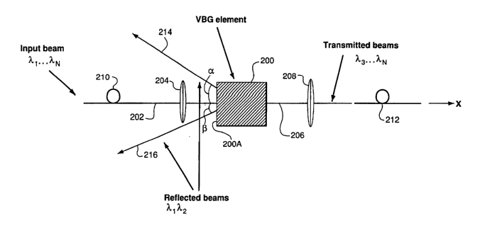
[0017] FIG. 2 demonstrates the transparency property of a VBG.
[0018] FIG. 3 is a schematic of a device according to the invention for
combining a
plurality of optical inputs into a single optical fiber output.
[0019] FIG. 4 is a perspective view of a preferred embodiment of a device
according to
the invention.
-4-
CA 02479467 2004-09-15
WO 03/079058 PCT/US03/08162
[0020] FIG. 5 depicts the interior of a device such as shown in FIG. 4.
[0021] FIG. 6 is a perspective view of another preferred embodiment of a
device
according to the invention.
[0022] FIG. 7 is a schematic diagram of a device such as shown in FIG. 6.
[0023] FIG. 8 is a perspective view of another preferred embodiment of a
device
according to the invention.
[0024] FIG. 9 is a schematic diagram of a DWDM multi-source combiner according
to
the invention.
[0025] FIG. 10 is a schematic diagram of an optical add-drop multiplexer
according to
the invention.
[0026] FIG. 11 is a schematic diagram of a multi-channel wavelength monitor
according to the invention.
[0027] FIG. 12 depicts chain cascading of a plurality of VBGs in a fiber optic
device
according to the invention.
[0028] FIG. 13 depicts lamination cascading of a plurality of VBGs in a fiber
optic
device according to the invention.
[0029] FIG. 14 depicts a multiple path device according to the invention.
[0030] FIG. 15 depicts a method according to the invention for fabricating
VBGs.
[0031] FIGS. 16A-C depict another method according to the invention for
fabricating
VBGs.
[0032] FIG. 17 depicts yet another method according to the invention for
fabricating
VBGs.
[0033] FIG. 1 ~ depicts an integrated VBG "chip" according to the invention.
DETAILED DESCRIPTION OF ILLUSTRATIVE EMBODIMENTS
Using sensitized silica glasses for manufacturing of VBG filters
[0034] One of the major problems in developing and using any kind of permanent
VBG
filters for practical applications has been the unavailability of a material
or a class of materials
possessing physical properties that are adequate for the practical
applications. For example, the
photorefractive electro-optic crystals, in which much of the research was
conducted on the
subject of VBGs, among other problems, are incapable of providing truly
permanent, stable
recording across a wide temperature range. Furthermore, these crystals are
strongly anisotropic,
which limits their usage substantially. For these reasons, an entire range of
applications of VBG
filters in general has not been substantially explored. In fact, to the
inventors' knowledge, there
is not a single photonic device now in the market that uses VBG elements.
-5-
CA 02479467 2004-09-15
WO 03/079058 PCT/US03/08162
[0035] According to the invention, a previously unexplored class of materials,
the
silicate photorefractive glasses (PRG), can be used to enable the design and
manufacturing of
practical devices based on VBGs, with special emphasis on photonic devices for
fiber-optic
applications. This type of materials substantially overcomes all of the above-
mentioned
drawbacks of the previously studied materials and possesses all the required
properties to
manufacture devices for demanding applications exemplified by the fiber
optics. These
properties include, but are not limited to, the following: a) optical
transparency in the entire
optical window from UV to mid-infrared; b) outstanding longevity of the
recorded gratings; c)
outstanding thermal stability (> 200 C); d) adequate dynamic range; e)
excellent optical quality,
including the achievable polishing quality of the elements made of this
material; d) low
manufacturing costs; e) ability to be formed and processed in the adequate
shapes and sizes (e.g.,
flat disks or wafers); f) refractive index isotropy. Compositions and
processes for manufacturing
such PRGs are described in U.S. Patent No. 4,057,408, the disclosure of which
is hereby
incorporated herein by reference in its entirety.
Manufacturing of VBG elements in silica glasses by recording holographically
at a
specific wavelength and using them in fiber-optic devices at an arbitrary
wavelength
[0036] As described in the literature on the theory of Bragg diffraction in
thick
holograms (see, e.g., Kogelnik, H., "Coupled wave theory for thick hologram
gratings," The Bell
System Technical Journal, November 1969, 48(9), 2909-2947), there are two
basic types of the
VBGs - transmission and reflection, which are different in their mode of
operation (see Kogelnik
Fig. 4).
[0037] FIG. 1A depicts a reflective VBG 102 having a grating wave vector, A,
in the
horizontal direction as shown. An input light beam 104 composed of light of a
plurality of
wavelengths ~,1, ... ~,N is directed toward the VBG 102 at a first angle a to
the input face 102A of
the VBG 102. The VBG 102 is formed such that it is transparent to all but one
of the
wavelengths ~,1, ... ?~N. That is, the light beam propagates through the
grating relatively
unaffected, except that the light having a certain wavelength, ~,1, is
filtered out of the beam. As a
result, only that light 106 having wavelengths ~,Z, ... ~,N continues through
the VBG 102 and exits
the VBG 102 at a second angle (3 to the output face 102B of the VBG 102.
Preferably, the VBG
102 is fabricated so that the angle (i at which the beam exits the VBG 102 is
as near as possible
to the angle a at which it entered the VBG 102 (i.e., the beam continues along
in a generally
straight line). Light 108 having wavelength ~,1, however, is reflected back at
an angle y from the
input face 102A of the VBG 102 because of the holography within the VBG 102.
That is, the
VBG 102 is fabricated such that the index of refraction varies within the VBG
102 to allow light
-6-
CA 02479467 2004-09-15
WO 03/079058 PCT/US03/08162
having wavelengths ~,2, ... ~,N to continue through the VBG 102, and light
having wavelength ~,1
to be reflected back at a known angle. Methods for fabricating such VBGs are
discussed in
detail below.
[0038] FIG. 1B depicts a transmissive VBG 112 having a grating wave vector, A,
in the
vertical direction as shown. An input light beam 114 composed of light of a
plurality of
wavelengths ~,1, ... ~,N is directed toward the VBG 112 at a first angle a to
the input face 112A of
the VBG 112. The VBG 112 is formed such that it is transparent to all but one
of the
wavelengths. That is, the light beam propagates through the grating relatively
unaffected, except
that the light having a certain wavelength, y, is filtered out of the beam. As
a result, only that
light 116 having wavelengths ~,2, ... ~,N continues through the VBG 112 and
exits the VBG 112 at
a second angle ~ to the output face 112B of the VBG 112. Preferably, the VBG
112 is fabricated
so that the angle (3 at which the beam 116 exits the VBG 112 is as near as
possible to the angle a
at which it entered the VBG 112 (i.e., it continues along in a generally
straight line). Light 118
having wavelength ~,1, however, exits the VBG 112 at a third angle y to the
output face 112B
because of the holography within the VBG 112. That is, the VBG 112 is
fabricated such that the
index of refraction varies within the VBG 112 to allow light having
wavelengths 7~2, ... ~,N to
continue relatively straight through the VBG 112, and light having wavelength
?~1 to be deflected
as it passes through the VBG 112 such that it exits the VBG 112 at a known
angle (3 to the output
face.
[0039] Wavelength filtering properties of transmission and reflection VBGs are
different primarily in the width of the filter that can be constructed in an
element of practical
size. Generally, reflection thick volume holograms have very narrow wavelength
bandwidth,
with the upper limit determined by the dynamic range of the material, as
described above in
connection with the example of lithium niobate VBG filters. Conversely,
transmission thick
volume holograms generally have wider bandwidth, which, historically, has
precluded their use
for the generation of white light color display holograms.
[0040] Nonetheless, when recorded in a sufficiently thick slab of a
transparent material
(e.g., > 1 mm), a method can be devised to record transmission VBGs that can
achieve
bandwidths sufficiently narrow for practical photonic devices (e.g., bandwidth
of 30 nm or less).
[0041] Another principal difference between reflection VBGs and transmission
VBGs
is that the transmission type allows tuning of the central wavelength of the
filter by adjusting the
incident angle of light upon the VBG. For that reason, a VBG filter can be
recorded at one
wavelength (e.g., in the UV range where silicate PRGs are sensitive) and
operate at another (e.g.,
in the 850 nm to 1650 nm range typically employed in various fiber-optic
devices). This can be
CA 02479467 2004-09-15
WO 03/079058 PCT/US03/08162
achieved without the limitations of recording through an orthogonal side of
the element,
described above for the case of the lithium niobate VBG filters. This means
that: a) the range of
the usable wavelengths is practically unlimited; b) wider bandwidths are
readily available; c)
there is no need for polishing additional surfaces.
[0042] The use of permanent transmission VBGs as band-pass filters for
manipulation
of wavelengths in photonic devices, exemplified by the fiber-optic active and
passive
components, has not been explored so far probably for one or more of the
following reasons: a)
strong anisotropy of the material (e.g., inorganic electro-optic
photorefractive crystals); b)
impossible to manufacture in sufficiently thick layers (> 1 mm, e.g., I~CG);
c) impossible to
achieve sufficient optical quality of the bulk material and/or polishing
quality of the surfaces
(e.g., photo-polymers); d) insufficient temperature stability.
[0043] FIG. 2 demonstrates the transparency property of a VBG 200 in which an
input
light beam 202 composed of light of a plurality of wavelengths ~,1, ... ~,N is
directed toward the
VBG 200, through a lens 204, along an optical axis, x, of the device. As
shown, the input light
beam 202 can be emitted from an optical fiber 210. The VBG element 200 is
fabricated such
that the index of refraction varies within the VBG 200 to allow light 206
having wavelengths ~,3,
... ~,N to continue relatively straight through the VBG 200, through a lens
208, and into a receiver
212, which can be another output optical fiber, for example, as shown. Light
214 having
wavelength ~,1, however, is reflected back at a first angle a from the input
face 200A of the VBG
200. Similarly, light 216 having wavelength ~,2 is reflected back at a second
angle (3 from the
input face 200A of the VBG 200 because of the holography within the VBG 200.
[0044] FIGS. 3-5 depict a preferred embodiment of a fiber optic device 300
according
to the invention for combining a plurality of optical fiber inputs 311-314
into a single optical
fiber output 310. As shown, the device 300 includes four optical inputs 311-
314, which can be
optical fibers, for example. Each optical input 311-314 carries light 301-304
of a different
wavelength ~,1-~,4. The device 300 also includes three VBG elements 330, 332,
334. . Light 301
from the first input 311, having wavelength ?~1, is transmitted into the
interior of the device 300,
where it is deflected via a first deflector 320 (such as a mirror, for
example) such that it enters
the first VBG element 330 at a known angle. As shown, the light travels along
the optical axis of
the device, and enters the VBG 330 at an angle of 90° to the input face
of the VBG 330. The
first VBG 330 is transparent to light having wavelength ~.1, so the light
having wavelength ~,1
exits the first VBG 330 at an angle of 90° with the output face of the
VBG 330.
[0045] Light 302 from the second input 312, having wavelength ~,2, is
transmitted into
the interior of the device 300, where it is deflected via a second deflector
322 such that it enters
_8_"
CA 02479467 2004-09-15
WO 03/079058 PCT/US03/08162
the first VBG element 330 at a known angle. The first VBG 330 deflects the
light having
wavelength ~,a such that the light having wavelength ~,Z exits the first VBG
330 at an angle of 90°
with the output face of the VBG 330 and, therefore, is combined with the light
having
wavelength ~,1.
[0046] Similarly, light 303 from the third input 313, having wavelength ~,3,
is
transmitted into the interior of the device 300, where it is deflected via a
third deflector 324 such
that it enters the second VBG element 332 at a known angle. The second VBG 332
deflects the
light having wavelength ~,3 such that the light having wavelength ~,3 exits
the second VBG 332 at
an angle of 90° with the output face of the second VBG 332. The second
VBG 332 is transparent
to light having wavelength ?~1 or ~,z. Consequently, the light having
wavelength ~,3 is combined
with the light having wavelength ~,1 and ~,a.
[0047] Similarly, light 304 from the fourth input 314, having wavelength ~,4,
is
transmitted into the interior of the device 300, where it is deflected via a
fourth deflector 326
such that it enters the third VBG element 334 at a known angle. The third VBG
334 deflects the
light having wavelength ~,4 such that the light having wavelength ~,4 exits
the third VBG 334 at
an angle of 90° with the output face of the third VBG 334. The third
VBG 334 is transparent to
light having wavelength ~,1, 7~2, or ~,3. Consequently, the light having
wavelength 7~4 is combined
with the light having wavelength ~,1, ~,Z, and ~,3.
[0048] Thus, an output light beam 306 composed of light have wavelengths ~,1,
?~2, ~3,
and ~,4 can be formed using a plurality of VBG elements. The output light beam
306 is received
by an optical receiver 310, such as an optical fiber. It should be understood
that, by reversing the
direction of the light flow, a device as shown in FIG. 5 can be used to
generate a plurality of
output light beams, each having a known wavelength, from an input light beam
composed of
light having a plurality wavelengths.
[0049] FIGS. 6 and 7 depict a preferred embodiment of a triplexer bi-
directional
transmitter/ receiver 600 according to the invention. As shown, the device 600
includes an
optical input 613, two optical outputs 611, 612, and a bi-directional optical
carrier 614, each of
which can be an optical fiber, for example. The bi-directional carrier 614
carries light 604
having wavelengths ~,1 ... ~,3 as shown. The first output 611 carries light
601 of wavelength ~,1 to
a first receiver 621. The second output 612 carries light 602 of wavelength
~,z to a second
receiver 622. The optical input 613 carries light 603 of wavelength ~,3 from a
source 623.
[0050] The VBG 610 is fabricated such that it is transparent to light having
wavelength
~,3, which is transmitted to the VBG 610 via the optical input 613. The VBG
610 can also be
fabricated such that it deflects light 601 having wavelength ~,1 and light 602
having wavelength
-9-
CA 02479467 2004-09-15
WO 03/079058 PCT/US03/08162
~,a. The light 601 having wavelength 7~1 can be received by a first optical
receiver 621, and the
light having wavelength ~,Z can be received by a second optical receiver 622.
The bi-directional
carrier 614 carries light 604 having wavelength ~,1 and wavelength ~.a in a
first direction (toward
the VBG) and wavelength ~,3 in a second direction (away from the VBG).
[0051] FIG. 8 depicts a preferred embodiment of a Xenpak form-factor CWDM
transmitter 800 according to the invention. As shown, the device 800 includes
an optical input
811 and four optical outputs 812-815, each of which can be an optical fiber,
for example. The
optical input carries light having wavelengths 7~1 ... ~,4. The first output
811 carnes light of
wavelength ~,1; the second output 812 carries light of wavelength ~,2; the
third output 813 carries
light of wavelength ~,3; and the fourth output 814 carries light of wavelength
7~4.
[0052] FIG. 9 is a schematic diagram of a DWDM multi-source combiner 900
according to the invention. As shown, the mufti-source combiner 900 includes
four optical
inputs 911-914, such as optical fibers, for example. Each optical input 911-
914 carnes light of a
different wavelength ~,1, ... ~,4 as shown. The device 900 also includes two
VBG elements 932,
934. Light 901 from the first input 91 l, having wavelength ~,1, is
transmitted, preferably through
a lens 921, such that it enters the first VBG element 932 at a first known
angle a. The first VBG
932 is fabricated such that the light 901 having wavelength ~,1 is deflected
from the first VBG
932 along the optical axis x of the device 900. Similarly, light 902 from the
second input 912,
having wavelength 7~2, is transmitted, preferably through a lens 922, such
that it enters the first
VBG element 932 at a second known angle (3. The first VBG 932 is fabricated
such that the light
902 having wavelength ~,a is also deflected from the first VBG 932 along the
optical axis x of the
device 900.
[0053] Light 903 from the third input 913, having wavelength ~,3, is
transmitted,
preferably through a lens 923, such that it enters the second VBG element 934
at a third known
angle y. The second VBG 934 is fabricated such that the light 903 having
wavelength ~,3 is
deflected from the VBG 934 along the optical axis x of the device 900.
Similarly, light 904 from
the fourth input 914, having wavelength ~,4, is transmitted, preferably
through a lens 924, such
that it enters the second VBG element 934 at a fourth known angle 8. The
second VBG 924 is
fabricated such that the light 904 having wavelength ~,4 is also deflected
from the second VBG
924 along the optical axis x of the device 900. The first VBG 932 is
transparent to light having
wavelength ~,3 and ~,4. Thus, light beams having respective wavelengths ~,1,
~,a, ~3, and ~,a can be
combined into a single optical beam 905, which can then be transmitted,
preferably through a
lens 925, to an optical receiver 915, such as an optical fiber, for example.
-10-
CA 02479467 2004-09-15
WO 03/079058 PCT/US03/08162
[0054] FIG. 10 is a schematic diagram of a free-space optical add-drop
multiplexer
(OADM) 1000 according to the invention. As shown, the OADM 1000 includes an
optical input
1011, such as an optical fiber, for example, that carries light 1001 having
wavelengths.7~l, ... 7~N
as shown. As shown in FIG. 10, the OADM 1000 includes a VBG element 1020 that
is
fabricated to reflect light 1002 having wavelength ~,1. The VBG 1020 is
transparent to light
having wavelengths ?~2, ... ~,N. The light beam 1001 from the first input 1011
is incident onto the
VBG 1020 at a first angle a to a first face 1020A of the VBG element 1020.
Consequently, a
light beam 1002 having wavelength ~,1 is deflected at a second angle (3 from
the face 1020A of
the VBG element 1020. The light beam 1002 having wavelength ~,1 is thus
"dropped" from the
input signal, and can be directed to an optical receiver 1012, such as another
optical fiber, for
example.
[0055] The OADM 1000 also includes an additional input 1013, which can be an
optical fiber, for example, that carries a light beam 1003 having wavelength
~,N+i. The light
beam 1003 having wavelength ~,N+i is incident onto the VBG 1020 at an angle ~y
to a second face
1020B of the VBG 1020. The VBG element 1020 is fabricated to reflect light
having
wavelength ~,N+i from the second face 1020B such that the light 1003 from the
additional input
1013 is combined with the light from the first input to form an output light
beam 1004 having
wavelengths ~,2, ... 7~N+i. The output light beam 1004 can be directed to an
optical receiver 1014,
such as another optical fiber, for example.
[0056] FIG. 11 is a schematic diagram of a mufti-channel wavelength monitor
1100
according to the invention. As shown, the mufti-channel wavelength monitor
1100 includes an
optical input 1115 that carries light 1005 having wavelengths ~,1, ... ~,N.
The monitor 1100 also
includes two VBG elements 1132, 1134. The input light beam 1105 is
transmitted, preferably
through a lens 1125, such that it enters the first VBG element 1132 at a first
known angle
(preferably, along the optical axis x of the device 1100, that is, 90°
to the face 1132A of the first
VBG 1132). The first VBG 1132 is fabricated such that the light 1101 having
wavelength ~,1+O
is deflected from the first VBG 1132 at a first angle a, and light 1102 having
wavelength ~,1-~ is
deflected from the first VBG 1132 at a second angle (3. The first VBG 1132 is
transparent to the
rest of the wavelengths in the input beam 1105. Light 11 O1 having wavelength
7~1+0 may be
received by an optical receiver 1111, and light 1102 may be received by an
optical receiver 1112.
[0057] The light beam is then transmitted to the second VBG element 1134,
which is
fabricated such that the light 1103 having wavelength ~.2+O is deflected from
the second VBG
1134 at a first angle y, and light 1104 having wavelength ~,2-O is deflected
from the second VBG
1134 at a second angle ~. Light 1103 having wavelength ~,2+~ may be received
by an optical
-11-
CA 02479467 2004-09-15
WO 03/079058 PCT/US03/08162
receiver 1113, and light 1104 having wavelength ~,2-0 may be received by an
optical receiver
1114. The second VBG 1134 is transparent to the rest of the wavelengths in the
beam. The
output beam 1106 can then be received, preferably through a lens 1126, by an
optical receiver
1116, which can be another optical fiber, for example.
[0058] Methods for packaging devices with large channel counts using VSG
filters
. [0059] One of the main advantages of VBG filters and, indeed, their unique
property is
the ability to record multiple filters sharing the same volume of the
material. This allows for the
fabrication of devices of very small size and unique functionality.
Nevertheless, the number of
gratings that can share the same volume, known as the multiplexing number, or
the M/#, in the
holographic memory field, is limited by the dynamic range of the material. For
that reason, for
practical materials suitable for manufacturing of VBG filters, that number
will typically be rather
limited (a realistic estimate is around 4 filters for a 4 mm thick element).
Furthermore,
fabrication of VBG filters with a larger number of gratings becomes
progressively more
complex, while at the same time reducing the flexibility in packaging them in
a device. In
addition, when sharing the same volume, the combined effect of the VBGs can be
obtained via
the coherent addition of the effects of the individual gratings, which results
in the appearance of
cross-terms, leading sometimes to undesirable side effects. It is, therefore,
desirable to have a
practical method for manufacturing devices with sufficiently large channel
count. According to
one aspect of the invention, fiber optic devices can be fabricated which can
have a basically
unlimited number of channels while using very simple VBG elements as building
blocks.
[0060] FIG. 12 depicts a device according to the invention in which any number
of
transmissive VBG filters can be combined to construct a device with an
arbitrary channel count
and for an arbitrary set of wavelengths. Preferably, the VBG filters are
identical, thereby
reducing the cost of fabrication. In this approach, the individual VBG
elements are positioned
on the main optical axis of the device and their tilt angles are adjusted
individually in order to
tune it to the peak wavelength of the desired channel. This approach may be
referred to as
"chain cascading."
[0061] As shown in FIG. 12, an optical input 1214 carries light 1204 having
wavelengths ?~1, ... ~,N. Light 1204 is incident on a first VBG element 1232
along the optical axis
x of the device. The first VBG 1232 is fabricated such that the light 1201
having wavelength ~,i
is deflected from the first VBG 1232 at a first angle a to the exit face 1232B
of the VBG 1232.
As shown, the VBG 1232 is positioned such that its grating vector A and exit
face 1232B are
perpendicular to the optical axis x of the device. Thus, the light 1201 having
wavelength ~,1 is
deflected from the first VBG 1232 at an angle 90-a to the optical axis x of
the device. The
-12-
CA 02479467 2004-09-15
WO 03/079058 PCT/US03/08162
device may include a first optical receiver 1211 that receives the deflected
beam 1201. The first
VBG 1232 is transparent to the rest of the wavelengths ~,2, ... ~,N in the
input beam 1204, such
that a transmitted beam 1205 having wavelengths ~,a, ... 7~N is transmitted
through the VBG 1232
along the optical axis x.
[0062] The transmitted beam 1205 is incident on a second VBG element 1234. The
second VBG 1234 may be fabricated, like the first VBG 1234, such that light
having wavelength
~,1 would be deflected from the second VBG 1234 at a first angle a to the exit
face 1234B of the
VBG 1234. As shown, the VBG 1234 is positioned such that its grating vector A
and exit face
1234B are at a known angle 0 (> 90°) to the optical axis x of the
device. Light 1202 having
wavelength ~,2 is deflected from the second VBG 1234 at a known angle [3 to
the exit face 1234B
of the VBG 1234 (and, therefore, at a known angle to the optical axis x). The
device may
include a second optical receiver 1212 that receives the deflected beam 1202.
The second VBG
1234 is transparent to the rest of the wavelengths ~,3, ... ~,N in the
transmitted beam 1205, such
that a second transmitted beam 1206 having wavelengths ~,3, ... 7~N is
transmitted through the
VBG 1234 along the optical axis x.
[0063] The transmitted beam 1206 is incident on a third VBG element 1236. The
third
VBG 1236 may be fabricated, like the first VBG 1232, such that light having
wavelength ~,1
would be deflected from the third VBG 1236 at a first angle a to the exit face
1236B of the VBG
1236. As shown, the VBG 1236 is positioned such that its grating vector A and
exit face 1236B
are at a known angle cp (<90°) to the optical axis x of the device.
Light 1203 having wavelength
~,3 is deflected from the third VBG 1236 at a known angle y to the exit face
1236B of the VBG
1236 (and, therefore, at a known angle to the optical axis x). The device may
include a third
optical receiver 1213 that receives the deflected beam 1203. The third VBG
1236 is transparent
to the rest of the wavelengths ?~4, ... ~,N in the transmitted beam 1206, such
that a third transmitted
beam 1207 having wavelengths ~,4, ... ~,N is transmitted through the VBG 1236
along the optical
axis x. The device may include a fourth optical receiver 1215 that receives
the transmitted beam
1207.
[0064] FIG. 13 depicts a device according to the invention that includes a
complex
VBG filter element that has been fabricated from a number of simple, possibly
identical, VBG
elements. In function it is similar to the device described above in
connection with FIG. 12 but
instead of being positioned and adjusted individually in the package, the
elements can be
properly positioned in a suitable fixture in direct physical contact with one
another and then
permanently bonded together, using suitable bonding materials that are well
known in the art,
thus creating a single compounded element with complex functionality.
-13-
CA 02479467 2004-09-15
WO 03/079058 PCT/US03/08162
[0065] The positioning of the individual VBG elements with respect to one
another in
such an arrangement can be important to the usefulness of the assembly.
Methods of exercising
such control can include: a) proper surface preparation of the wafers of the
recording material,
such as polishing, parallelism of the surfaces etc.; b) proper rotational
orientation of the elements
with respect to each other during the bonding procedure; c) use of calibrated
spacers to the adjust
relative angle between the individual VBG elements; d) precise control of the
tilt angle of the
wafer with respect to the recording laser beams during the holographic
recording process.
[0066] This approach, referred to as "lamination cascading," enables the
achievement
of the same density of the grating packing in the same package volume as the
direct multiplexing
of the filters during the recording process, but without the need of multiple
exposures and
without the physical overlap, and thus interference, of the individual filters
in the bulk of the
material.
[0067] As shown in FIG. 13, an optical input 1314 carries light 1304 having
wavelengths ~,1, ... ~,N. Light 1304 is incident on a series of VBG elements
1332-1334 along the
optical axis x of the device. The VBG elements 1332-1334 are fabricated such
that light 1301
having wavelength ~,l is deflected from the third VBG 1334 at a first angle a
to the exit face
1334B of the VBG 1334, light 1302 having wavelength ~.a is deflected from the
third VBG 1334
at a second angle (3 to the exit face 1334B of the VBG 1334, and light 1303
having wavelength
~,3 is deflected from the third VBG 1334 at a third angle y to the exit face
1334B of the VBG
1334. The device may include a first optical receiver 1311 that receives the
deflected beam
1301, a second optical receiver 1312 that receives the deflected beam 1302,
and a third optical
receiver 1313 that receives the deflected beam 1303. The VBGs 1332-1334 may be
transparent
to the rest of the wavelengths ~,4, ... ~,N in the input beam 1304, such that
a transmitted beam 1305
having wavelengths ~,4, ... ~,N is transmitted through the VBGs 1332-1334
along the optical axis
x. The device may include a fourth optical receiver 1314 that receives the
transmitted beam
1304.
[0068] FIG. 14 depicts a device according to the invention in which any
simple,
individual VBG element can be used for processing several wavelength channels
by allowing
multiple paths through it in different directions. In its simplest form, the
so-called "double pass
configuration" functions as follows:
[0069] A series of simple individual VBG elements is positioned in line as
described
above in connection with FIG. 12. A mirror is placed at the end of the chain
of the elements,
which reflects the transmitted light back onto the same elements. This has the
effect of folding
the chain of the elements back onto itself. The mirror angle is adjusted
slightly, so that the angle
-14-
CA 02479467 2004-09-15
WO 03/079058 PCT/US03/08162
of the back-reflected light is somewhat different than the forward-propagating
light. This angle
is adjusted in such a way as to tune the center wavelength of the VBG filters
to the desired value.
[0070] In such an implementation, the method allows using each of the VBG
elements
more than once, thus effectively increasing the number of filters without
increasing the number
of VBG elements, and thereby enabling the overall size of the package to
remain practically the
same. Multiple path folding is also possible if an additional mirror is used
in the beginning of
the chain of the VBG elements, slightly offset from the axis in angle and
space.
[0071] As shown in FIG. 14, an optical input 1415 carries light 1405 having
wavelengths ~,1, .... ~,N. Light 1405 is incident on a first VBG element 1432
along the optical axis
x of the device. The first VBG 1432 is fabricated such that light 1401 having
wavelength 7~1 is
deflected from the first VBG 1432 at an angle a to the exit face 1432B of the
first VBG 1432.
The first VBG 1432 is transparent to the rest of the wavelengths ~,2, ... ~,N
in the input beam 1405,
such that a transmitted beam 1406 having wavelengths ~,a, ... ~,N is
transmitted through the VBG
1432 along the optical axis x.
[0072] The transmitted beam 1406 is incident on a second VBG element 1434. The
second VBG 1434 is fabricated such that light 1402 having wavelength 7~2 is
deflected from the
second VBG 1434 at an angle /3 to the exit face 1434B of the second VBG 1434.
The second
VBG 1434 is transparent to the rest of the wavelengths ~,3, ... ~,N in the
transmitted beam 1406,
such that a transmitted beam 1407 having wavelengths ~,3, ... ~,N is
transmitted through the VBG
1434 along the optical axis x.
[0073] The transmitted beam 1407 is directed toward a mirror 1420, which is
disposed
at an angle cp to the optical axis x of the device. The reflected beam 1408 is
incident on the
second VBG 1434 at an angle cp to the exit face 1434B. The second VBG 1434 is
fabricated
such that light 1403 having wavelength ~.3 is deflected from the second VBG
1434 at an angle y
to the entrance face 1434A of the second VBG 1434. The second VBG 1434 is
transparent to
the rest of the wavelengths ~,4, ... ~,N in the reflected beam 1408, such that
a reflected beam 1409
having wavelengths ~,4, ... ~,N is transmitted through the VBG 1434.
[0074] The reflected beam 1409 is incident on the first VBG 1432 at an angle
cp to the
exit face 1432B. The first VBG 1434 is fabricated such that light 1404 having
wavelength ~,4 is
deflected from the first VBG 1432 at an angle 8 to the entrance face 1432A of
the first VBG
1432. The first VBG 1432 is transparent to the rest of the wavelengths ~,5,
... ~,N in the reflected
beam 1409, such that a reflected beam 1410 having wavelengths ~,5, ... ~,N is
transmitted through
the VBG 1432.
-15-
CA 02479467 2004-09-15
WO 03/079058 PCT/US03/08162
[0075] The device may include a first optical receiver that receives the
deflected beam
1401, a second optical receiver that receives the deflected beam 1402, and a
third optical receiver
that receives the deflected beam 1403, and a fourth optical receiver that
receives the deflected
beam 1404. The device may also include a fifth optical receiver that receives
the reflected beam
1410.
[0076] It should be understood that any of the techniques described above can
be
optimized to take maximum advantage of VBG properties such as: transparency to
all but one
wavelength, angular tunability, functionality distributed over the volume of a
thick material,
material rigidity and dimensional stability, excellent polishing qualities,
and the like.
Methods for economically manufacturing VBG elements
[0077] In the manufacturing of VBG elements, it is typically desirable to
minimize the
costs of production of such elements. For that reason, holographic recording
of each element
individually is likely to be cost-prohibitive for most or all of the high-
volume applications. A
number of methods according to the invention for cost-effective production of
such elements will
now be described.
[0078] A first such method, depicted in FIG. 15, exploits the unique property
of a
hologram, whereupon each fractional piece of the recorded hologram possesses
full and
complete information about the recorded object. When applied to the VBG
filters recorded on
the PRG plates, it means that each piece of such plate, or wafer, should have
the same filtering
properties as the wafer in whole. For that reason, a large-size wafer 1500 can
be diced, using a
suitable cutting device, such as a saw, for example, into a large number of
relatively small
individual VBG elements 1502, each with complete filter functionality. In
following this
process, one could significantly reduce the number of recording and testing
operations, thereby
reducing the manufacturing costs of the VBG elements.
[0079] A second cost-reduction method according to the invention applies to
the
repetitive fabrication of the filter with identical properties. Such an
approach is particularly
suitable for high-volume production environments. In such circumstances
reproduction of a
filter with a complex shape, which may require, for example, multiple exposure
steps to achieve
the complete control over its spectral shape, may result in a prohibitively
long and complex
manufacturing operations. However, since holography allows true and complete
reconstruction
of the recorded wavefront, it is, therefore, possible to record a hologram of
the reconstructed
wavefront, rather than the true original, to achieve the same result.
[0080] This approach includes: a) placing a "virgin" recording wafer directly
behind a
recorded "master" hologram; and b) directing the reference beam onto the
master hologram in
-16-
CA 02479467 2004-09-15
WO 03/079058 PCT/US03/08162
exactly the same fashion as during the recording of the master. The
transmitted reference wave
and the reconstructed obj ect wave interfere again behind the master hologram.
Consequently, a
new hologram is recorded on the virgin wafer, which is an exact replica of the
master.
[0081] The advantages of this method include but are not limited to the
following: a)
better stability (not sensitive to the phase fluctuations); b) simpler setup
(no filter shape control
required); c) no polishing on the virgin wafer is required, if it is placed in
direct contact with the
master and an index matching fluid is used on the interface; and d) shorter
cycle times (higher
throughput).
Methods to control the filter response function
[0082] When used in practical applications such as in fiber-optic devices, for
example,
the spectral shape of a filter can be used to manipulate the wavelengths of
light in a desired
fashion. The filter shape can determine such device parameters as adjacent
channel isolation,
cross-talk, suppression ratio, etc. The ability to control the spectral shape
of the VBG filters,
therefore, can make the difference between a practically usable device and a
practically useless
one.
[0083] As follows from the general theory of Bragg diffraction (see Kogelnik),
the
spectral shape of the filter created by a VBG is related via a Fourier
transform to the amplitude
and phase envelope of the VBG along the general direction of propagation of
the affected light
wave. It is, therefore, desirable to be able to control both in order to
create a filter with a desired
spectral shape.
[0084] A method according to the invention for controlling the spectral shape
of a VBG
filter relates to the use of the Fourier transform property of a lens and the
phase capturing ability
of the holographic recording method. As depicted in FIG. 16A, a method 1600
for creating a
VBG filter with any desired spectral shape can be performed as follows. A mask
1602
representing the desired filter shape is placed in the front focal plane of a
lens 1604 situated in
the object arm of the holographic recording setup. The recording media sample
1606 (e.g., a
glass wafer) is placed in the back focal plane of the same lens. The plane-
wavefront reference
beam of the holographic recording setup overlaps with the object beam on the
sample,
subtending it at an angle required by the target operational wavelength of the
VBG filter being
recorded.
[0085] When positioned as described, the lens creates a true Fourier transform
of the
mask directly on the recording medium. Via a coherent interference with the
plane reference
wave, both the amplitude and the phase of the Fourier transform are
transferred to the amplitude
and phase envelope of the VBG imprinted on the recording material. When
reconstructed, or
-17-
CA 02479467 2004-09-15
WO 03/079058 PCT/US03/08162
"read," with a light beam nearly normal to the recorded grating planes, the
spectral response of
the VBG filter thus recorded will take the shape of the masks placed in the
front focal plane of
the lens.
[0086] This method allows for a single exposure recording of a filter with
practically
arbitrary complexity of the shape of the spectral response function and is
referred to as the
"parallel method" or the "holographic filter imprinting method."
[0087] A holographic filter imprinting method according to the invention can
be
similarly applied to the task of shaping the filter response function of
transmission VBG filters.
It may be accomplished by choosing a proper orientation of the apodizing mask
relative to the
direction of the grating planes and, similarly, by choosing the proper
entrance and exit faces on
the VBG element.
[0088] Exemplary methods asks for creating transmissive and reflective VBGs
are
depicted in FIGS. 16B and 16C respectively. As shown, a mask 1612 having a
slit 1614 can be
placed in the front focal plane of the lens. Light shone through the mask will
generate a square
wave 1616. As the light passes though the lens, the Fourier transform 1618 of
the square wave
will be imprinted on the sample 1620. When reconstructed, the spectral
response of the pattern
1622 recorded on the VBG filter 1620 will take the shape of a square wave
1624. Depending on
the orientation of the mask relative to the grating plane, the VBG can be made
reflective (as
shown in FIG. 16B) or transmissive (as shown in FIG. 16C).
Method for controlling the shape of transmissive VBG filters
[0089] Furthermore, when dealing with VBG filters functioning in the
transmission
geometry, a different approach can be taken in order to manipulate the
spectral shape of the
filter. In this case, the method, which is depicted in FIG. 17, comprises
multiple, sequential
exposures of the same volume of the recording material. Each exposure would
produce a simple
plane VBG, but after recording multiple gratings a filter of an arbitrary
shape will be constructed
via coherent addition of the recorded VBGs. Volume Bragg gratings are physical
representations
of sinusoidal waves, and, therefore, their coherent sum is a Fourier transform
of an envelope
function.
[0090] For that reason, a close representation of an arbitrary amplitude and
phase
envelope fi~nction can be constructed via a series of holographic exposures,
provided appropriate
control is exercised over both the amplitude and the relative phase of the
gratings recorded in
such series of exposures. Such control can be achieved via employing
techniques for active
measurement and stabilization of the phase of the recorded VBGs.
-18-
CA 02479467 2004-09-15
WO 03/079058 PCT/US03/08162
[0091] As shown in FIG. 17, a virgin sample 1702 is subjected to a first pair
of incident
beams 1712 and 1714. Beam 1712 is incident on the entrance face 1702A of the
virgin sample
1702 at an angle a relative to the entrance face 1702A (and, as shown,
relative to the grating
vector A). Beam 1714 is incident on the entrance face 1702A of the virgin
sample 1702 at an
angle (3 relative to the entrance face 1702A (and, as shown, relative to the
grating vector A).
Thus, a first holographic sample 1704 is formed having a first holographic
image 1722.
[0092] The first holographic sample 1704 is then subjected to a second pair of
incident
beams 1716 and 1718. Beam 1716 is incident on the entrance face 1704A of the
first
holographic sample 1704 at an angle y relative to the entrance face 1704A
(and, as shown,
relative to the grating vector A). Beam 1718 is incident on the entrance face
1704A of the first
holographic sample 1704 at an angle 8 relative to the entrance face 1704A
(and, as shown,
relative to the grating vector A). Thus, a second holographic sample 1706 is
formed having a
second holographic image 1724.
VSG Chip
[0093] FIG. 18 depicts an integrated VBG "chip" according to the invention. As
shown, the VBG chip 1800 is a monolithic glass structure into which a
plurality of holographic
images or "gratings" have been recorded. An optical input 1815 carries light
1805 having
wavelengths ~,1, ... ~,N. Light 1805, which may be collimated, is incident on
a first grating 1822.
Grating 1822 is recorded such that light 1801 having wavelength ~,1 is
deflected at an angle such
that it is received by grating 1832. Grating 1832 is recorded such that it
deflects the light 1801
out of the chip 1800 toward an optical receiver 1811. Grating 1822 is
transparent to the rest of
the wavelengths ~,a, ... ~,N in the input beam 1805, such that a transmitted
beam 1806 having
wavelengths ~,a, ... ~,N is transmitted through the grating 1822.
[0094] The transmitted beam 1806 is incident on grating 1824, which is
recorded such
that light 1802 having wavelength 7~2 is deflected at an angle such that it is
received by grating
1834. Grating 1834 is recorded such that it deflects the light 1802 out of the
chip 1800 toward
an optical receiver 1812. Grating 1824 is transparent to the rest of the
wavelengths ~,3, ... ~,N in
the beam 1806, such that a transmitted beam 1807 having wavelengths ~.3, ...
~,N is transmitted
through the grating 1824.
[0095] Similarly, the transmitted beam 1807 is incident on grating 1826, which
is
recorded such that light 1803 having wavelength 7~3 is deflected at an angle
such that it is
received by grating 1836. Grating 1836 is recorded such that it deflects the
light 1803 out of the
chip 1800 toward an optical receiver 1813. Grating 1826 is transparent to the
rest of the
-19-
CA 02479467 2004-09-15
WO 03/079058 PCT/US03/08162
wavelengths ~,4, ... ~,N in the beam 1807, such that a transmitted beam 1808
having wavelengths
~,4, ... 7~N is transmitted through the grating 1826.
[0096] The transmitted beam 1808 is incident on grating 1828, which is
recorded such
that light 1804 having wavelength ~,4 is deflected at an angle such that it is
received by grating
1838. Grating 1838 is recorded such that it deflects the light 1804 out of the
chip 1800 toward
an optical receiver 1814. Grating 1828 is transparent to the rest of the
wavelengths ~,5, ... 7~N in
the beam 1808, such that a transmitted beam 1809 having wavelengths ~,5, ...
~,N is transmitted
through the grating 1828. The transmitted beam 1809 is directed toward an
optical receiver
1815. As shown, each of the optical receivers 1811-1814 and 1816 can be an
optical fiber, for
example. Any or all of the optical receivers 1811-1814 and 1816 can be bundled
together to
form an optical fiber ribbon, for example.
[0097] A VBG chip as shown can be made according to the following method. One
or
more incident beams are directed towaxd a first location of a virgin sample
(to form grating 1822,
for example). Then, the beams are turned off, and either the sample or the
source of illumination
is positioned (e.g., the sample may be moved laterally and/or rotationally as
necessary) such that
the incident beams) may now be directed toward a second location on the sample
(to form
grating 1824, for example). This process is repeated until all desired
gratings have been
recorded.
[0098] Thus, there have been described fiber optic devices comprising volume
Bragg
gratings and methods for fabricating the same. Those skilled in the art will
appreciate that
numerous changes and modifications can be made to the preferred embodiments of
the invention,
and that such changes and modifications can be made without departing from the
spirit of the
invention. Examples of devices that can be made in accordance with the
invention include,
without limitation, 1xN laser source combiners, mufti-channel transmit/receive
modules
(including triplexers), optical add-drop multiplexers, terminal multiplexers,
network monitors,
wavelength lockers, tunable filters, tunable gain equalizers, dispersion
compensators, and the
like.
-20-