Note: Descriptions are shown in the official language in which they were submitted.
CA 02479550 2004-09-16
WO 03/086026 PCT/US03/09851
TITLE
HOLE TRANSPORT POLYMERS AND DEVICES MADE WITH SUCH
POLYMERS
BACKGROUND OF THE INVENTION
Field of the Invention
This invention relates to polymeric materials having useful hole
transport properties. The polymers can also be electroluminescent. The
invention further relates to electronic devices in which the active layer
includes such polymeric materials.
Description of the Related Art
Organic electronic devices that emit light, such as light-emitting
diodes that make up displays, are present in many different kinds of
electronic equipment. In such devices, an organic active layer is
sandwiched between two electrical contact layers. At least one of the
electrical contact layers is light-transmitting so that light can pass through
the electrical contact layer. The organic active layer emits light through
the light-transmitting electrical contact layer upon application of
electricity
across the electrical contact layers.
It is well known to use organic electroluminescent compounds as
the active component in light-emitting diodes. Simple organic molecules
such as anthracene, thiadiazole derivatives, and coumarin derivatives are
known to show electroluminescence. Semiconductive conjugated
polymers have also been used as electroluminescent components.
Polymeric materials with stilbenyl or oxadiazole side chains have been
reported by Hoimes et al., U.S. Patent 5,653,914.
Many electroluminescent materials have poor charge transport
properties. To improve these properties additional charge transport
materials can be added to the light-emitting layer, or as a separate layer
between the light-emitting layer and an electrode. Hole transport materials
have frequently been employed. Known hole transport materials include
simple molecules such as N,N'-diphenyl-N,N'-bis(3-methylphenyl)-[1,1'-
biphenyl]-4,4'-diamine (TPD) and bis(4-(N,N-diethylamino)-2-
methylphenyl](4-methylphenyl)methane (MPMP), and polymeric materials
such as polyvinylcarbazole (PVK), (phenylmethyl)polysilane, poly(3,4-
ethylenedioxythiophene) (PEDOT), and polyaniline (PANI). It is also
known to use electron and hole transporting materials such as 4,4'-N,N'-
dicarbazole biphenyl (BCP); or light-emitting materials with good electron
and hole transport properties, such as chelated oxinoid compounds, such
CA 02479550 2004-09-16
WO 03/086026 PCT/US03/09851
as tris(8-hydroxyquinolato)aluminum (AIq3). Fused aromatic ring
compounds such as pentacene are known to be electron transport
materials. Copolymers having two different pendant aromatic groups have
been disclosed as light-emitting materials in US Patent 6,007,928.
There is a continuing need for new hole transport materials.
SUMMARY OF THE INVENTION
The present invention is directed to a hole transport polymer
including a polymeric backbone having linked thereto a plurality of
substituents that includes at least one fused aromatic ring group, with the
proviso that the polymer does not contain groups selected from
triarylamines and carbazole groups.
The invention is further directed to an organic electronic device
having an active layer between an anode and a cathode, wherein the
device further has at least one first hole transport polymer that includes a
polymeric backbone having linked thereto a plurality of substituents
including at least one fused aromatic ring group, with the proviso that the
polymer does not contain groups selected from triarylamines and
carbazole groups.
As used herein, the term "hole transport material" is intended to
mean material that can receive a positive charge from the anode and
move it through the thickness of the material with relatively high efficiency
and small loss. The term "hole transport polymer" is intended to mean
polymeric hole transport material. The term "polymer" is intended to
include homopolymers as well as copolymers having two or more different
repeating units. The term "functionalized polymer" is intended to mean a
polymer having at feast one functional groups) capable of reacting to
attach a fused aromatic ring group to the polymer backbone. The term
"functionalized fused aromatic ring compound" is intended to mean a fused
aromatic ring compound having at least one functional groups) capable of
reacting to attach to the polymer backbone. The term "photoactive" refers
to any material that exhibits electroluminescence and/or photosensitivity.
The term "(meth)acrylic" is intended to mean acrylic, methacrylic or
combinations. The term "(meth)acrylate" is intended to mean acrylate,
methacrylate, or combinations. In addition, the IUPAC numbering system
is used throughout, where the groups from the Periodic Table are
numbered from left to right as 1 through 18 (CRC Handbook of Chemistry
and Physics, 81St Edition, 2000).
2
CA 02479550 2004-09-16
WO 03/086026 PCT/US03/09851
BRIEF DESCRIPTION OF THE DRAWINGS
Figure 1 is a schematic diagram of a light-emitting device (LED).
Figure 2 is a current vs voltage curve for the device of Example 5.
Figure 3 is a current vs voltage curve and a light-emission vs
voltage curve for the device of Example 9.
DESCRIPTION OF THE PREFERRED EMBODIMENTS
The at least one fused aromatic ring group of the substituents
attached to the polymeric backbone generally has from 10 to 50 carbon
atoms and contain from 2 to 8 fused aromatic rings, preferably 2 to 4. The
fused aromatic ring group can optionally be substituted with alkyl or aryl
groups having 1 to 20 carbon atoms. Examples of suitable fused aromatic
ring groups include naphthyl, anthracyl, phenanthryl, phenalenyl, fluorenyl,
pyrenyl, and other tetracenyl and pentacenyl groups. In accordance to the
present invention, hole transport properties are achieved in the absence of
groups which are generally used to provide hole transport properties, such
as triarylamine groups and carbazole groups.
The hole transport polymers can be obtained by reacting a polymer
having a first type of reactive group ("functionalized polymer") with a fused
aromatic ring compound having a second type of reactive group
("functionalized fused aromatic ring compound"). This is shown
schematically in Reaction (1) below.
Pol-R~ + Ar-R2 = Pol-R3-Ar + (S) Reaction (1)
where Pol represents the polymeric backbone, Ar represents the fused
aromatic ring, R~ and R2 represent the first type and second type of
reactive groups, respectively, R3 represents the linkage resulting from the
reaction of R~ and R2. , and S represents any byproducts which may be
formed in the reaction.
Techniques for attaching small molecules to polymers are well-
known, as in the coupling of biochemical ligands to latex particles. This is
discussed in, for example, Uniform Latex Particles, by L. B. Bangs (Form
# 1661-84 from Seragen Diagnostics, Inc., Indianapolis, IN, 1984). For
example, a polymer having carboxylic acid functional groups can be
reacted with a fused aromatic ring compound having amino functional
groups, forming an amide linkage. Alternatively, the carboxylic acid group
can be on the fused aromatic ring and the amino group on the polymer.
Similarly, hydroxyl groups react with acid chloride groups to form ester
3
CA 02479550 2004-09-16
WO 03/086026 PCT/US03/09851
linkages. Other types of reactive pairs include hydroxyl and chloromethyl
groups; hydroxyl and carboxylic acid groups; isocyanate and hydroxyl or
amine groups; epoxy and amine groups; acid chloride and amine groups;
sulfonic acid and amine groups; suifonic acid chloride and hydroxyl
groups; aldehyde and amino groups; aldehyde and carboxyl groups;
aldehyde and hydroxyl groups; and aldehyde and methylketone groups. A
variety of reactions that will provide linkages are available in the synthetic
organic chemistry literature.
Alternatively, the hole transport polymer can be obtained by
polymerizing at least one type of monomer having attached thereto a
fused aromatic ring group ("functionalized monomer"), as shown in
Reaction (2) below.
Mon - R4 - Ar -~ Pol - R4 - Ar Reaction (2)
where Mon represents a polymerizable compound, R4 represents a linking
group, and Ar and Pol are as defined in Reaction (1) above.
I. Functionalized Polymer
The functionalized polymeric compounds that are useful in the
~ present invention can be generally described as having: (a) a polymeric
backbone; (b) a plurality of a first-type functional group; optionally (c) a
spacer group between the polymeric backbone and the first-type functional
group; and optionally (d) a plurality of second-type functional groups) that
are the same or different from each other. The polymeric backbone can
be any polymer or copolymer having the desired properties and
processability, and to which the fused aromatic ring groups can be
attached. Some categories of useful polymeric backbones include
polyacrylates; polymethacrylates; polyaramids; polystyrenes; polyarylenes;
polyvinylenes; polyvinyl ethers; and polyvinyl esters.
The first-type functional groups useful for attaching the fused
aromatic ring groups, are any of those discussed above as part of a
reactive pair.
The number of fused aromatic groups on the polymeric backbone,
which also can be described as the "density of fused aromatic groups", will
affect the efficiency of the polymer as a hole transport material. However,
when choosing the polymer, other factors should also be taken into
consideration, such as processability and film forming capability. For the
polymeric materials of the invention, the density of fused aromatic groups
4
CA 02479550 2004-09-16
WO 03/086026 PCT/US03/09851
is determined by the relative proportion of monomers having first-type
functional groups ("first-type functional monomers") to other monomers not
having first-type functional groups in the polymer. In general, the ratio of
first functional monomers to other monomers can be in the range of about
5:95 to 95:5.
The first-type functional group can be attached directly to the
polymer backbone, as, for example, the carboxyl group of a polyacrylic
acid polymer. However, it is also possible to have a spacer group
between the first-type functional group and the polymeric backbone.
Useful spacer groups are those that are chemically stable and do not
deleteriously affect the transport properties of the polymer. The spacer
group can be a saturated or unsaturated aliphatic group, or an aromatic
group. The spacer group can contain heteroatoms, particularly oxygen
and nitrogen. In some cases, a spacer group is present because the most
readily available monomers for certain first functional groups have the
spacer group. The spacer group generally has from 1 to 50 carbon atoms;
preferably from 5 to15 carbon atoms. The spacer group can simply
provide distance between the polymer backbone and first functional group,
or it can provide functionality, as discussed below.
The functionalized polymer can also have at least one second-type
functional group. The second-type functional group can be present to
modify the physical properties of the final polymer. Examples of such
types of groups include plasticizing groups, such as alkylene oxide groups,
and reactive and/or crosslinkab(e groups, such as terminal vinyl groups
and epoxy groups. The second-type functional group can be present in
the polymer backbone, in the spacer group attached to the first-type
functional group, or in pendant groups separate from the first-type
functional group.
The functionalized polymer can be made using monomers) having
the desired functional group(s), using conventional polymerization
techniques. Examples of suitable monomers include (meth)acrylic acid
(carboxyl functionality); 4-styrenecarboxylic acid (carboxyl functionality);
aminoalkyl acryiates and methacrylates (amino functionality); hydroxylalkyl
(meth)acrylates (hydroxy funcationality); glycidyl (meth)acrylate (epoxy
functionality); and similar monomers having the desired functional group.
The functionalized polymers can be a homopolymer or a copolymer.
The copolymers can be prepared so that they are random, alternating,
block, or comb copolymers. The process for forming these different
5
CA 02479550 2004-09-16
WO 03/086026 PCT/US03/09851
structural copolymers are well known in the art, and have been discussed
in, for example, Principles Of Polymerization, 3rd Edition, by George
Odian (John Wiley & Sons, New York, NY, 1991); Chemical Reactions of
Natural and Synthetic Polymers, by M. Lazar et al.; and Chemical
S Reactions on Polymers, by Benham and Kinstle (1988).
II. Functionalized Fused Aromatic Ring Compounds
Functionalized fused aromatic ring compounds have reactive
groups capable of reacting with groups on the functionalized polymer, as
discussed above. Useful types of functionalized fused aromatic ring
compounds include aromatic amines, aromatic sulfonyl chlorides,
aromatic isothiocyanates, aromatic succinimidyl esters, aromatic
aldehydes, and aromatic alcohols or phenols. Some of these compounds
are commercially available, such as 1-(1-naphthyl)ethylamine;
1-pyrenemethylamine; 1-pyrenepropylamine; 4'-(aminomethyl)fluorescein;
rhodamine B ethylene diamine; rhodamine B sulfonyl chloride; and
5-dimethylaminonaphthylene-1-sulfonyl chloride. Other suitable
functionalized fused aromatic ring compounds can be prepared using
standard synthetic chemical techniques.
III. Functionalized Monomers
In general, functionalized monomers can be prepared by coupling
the functional groups to monomers, using the same coupling chemistry as
described above. When the hole transport polymer is prepared from
functionalized monomers it is possible to get more structurally well-defined
polymeric materials. The functionalized monomers can be polymerized
using processes that result in different structures, such as block
copolymers, alternating copolymers, comb polymers, and other known
polymeric structures. When the hole transport polymer is prepared from a
functionalized polymer and functionalized fused aromatic ring compound,
the reactions occur in a more random, statistically controlled manner.
IV. Devices
The present invention also relates to an electronic device
comprising an organic active layer sandwiched between two electrical
contact layers, an anode and a cathode, wherein the device further
comprises the hole transport polymer of the invention. A typical structure
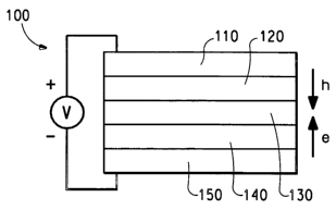
3S is shown in Figure 1. The device 100 has an anode layer 110 and a
cathode layer 150. Adjacent to the anode is an optional layer 120
comprising a hole transport material. Adjacent to the cathode is an
optional layer 140 comprising an electron transport material. Between the
6
CA 02479550 2004-09-16
WO 03/086026 PCT/US03/09851
anode and the cathode (or the optional charge transport layers) is the
organic active layer 130. The hole transport polymer of the invention is
present in the organic active layer 130, and/or in the hole transport layer
120. It is understood that each functional layer may be made up of more
than one layer.
The device generally also includes a support, which can be
adjacent to the anode or the cathode. Most frequently, the support is
adjacent the anode. The support can be flexible or rigid, organic or
inorganic. Generally, glass or flexible organic films are used as a support.
The anode 110 is an electrode that is particularly efficient for
injecting or collecting positive charge carriers. It can be made of, for
example materials containing a metal, mixed metal, alloy, metal oxide or
mixed-metal oxide, or it can be a conducting polymer. Suitable metals
include the Group 11 metals, the metals in Groups 4, 5, and 6, and the
Groups 8-10 transition metals, as shown on the periodic table of elements
(current IUPAC format). If the anode is to be light-transmitting, mixed-
metal oxides of Groups 2, 3, 4, 13 and 14 metals, such as indium-tin-
oxide. A conducting polymer, such as poly(3,4-ethylenedioxythiophene)
(PEDOT), and polyaniline (PANI) can be used when the conductivity is
greater than 10-2 S/cm. At least one of the anode and cathode should be
at least partially transparent to allow the passage of light into or out from
the active layer of the device.
Inorganic anode layers are usually applied by a physical vapor
deposition process. The term "physical vapor deposition" refers to various
deposition approaches carried out in vacuo. Thus, for example, physical
vapor deposition includes all forms of sputtering, including ion beam
sputtering, as well as all forms of vapor deposition such as e-beam
evaporation. A specific form of physical vapor deposition which is useful is
rf magnetron sputtering. The conductive polymer anode layers can be
applied using any conventional means, including spin-coating, casting,
and printing, such as gravure printing, ink jet printing or thermal
patterning.
The hole transport polymer of the invention can be present as a
separate layer 120, or in combination with the emitting material in layer
130. The polymer layer can be applied using any conventional application
means, as described above. The polymer is generally applied as a solution
or dispersion in organic solvents such as dimethyl sulfoxide, N-methyl
pyrrolidone, dimethyl formamide, acetonitrile, propylene carbonate,
propylene glycol monomethyl ether, dimethyl acetamide, and
7
CA 02479550 2004-09-16
WO 03/086026 PCT/US03/09851
tetrahydrofuran. The concentration of the polymer in the solvent is not
particularly critical, so long as the solution or dispersion can be coated to
form a continuous film. In general, solutions or dispersion having 1 to 5%
by weight of the polymer can be used.
In some cases it may be desirable to have an additional hole
transport layer (not shown) made from other hole transport materials.
Examples of other suitable hole transport materials for layer have been
summarized for example, in Kirk-Othmer Encyclopedia of Chemical
Technology, Fourth Edition, Vol. 18, p. 837-860, 1996, by Y. Wang. Both
hole transporting molecules and polymers can be used. Commonly used
hole transporting molecules are: N,N'-diphenyi-N,N'-bis(3-methylphenyl)-
[1,1'-biphenyl]-4,4'-diamine (TPD); 1,1-bis[(di-4-tolylamino)
phenyl]cyclohexane (TAPC); N,N'-bis(4-methylphenyl)-N,N'-bis(4-
ethylphenyl)-[1,1'-(3,3'-dimethyl)biphenylj-4,4'-diamine (ETPD); tetrakis-(3-
methylphenyl)-N,N,N',N'-2,5-phenylenediamine (PDA); a-phenyl-4-N,N-
diphenylaminostyrene (TPS); p-(diethylamino)benzaldehyde
diphenylhydrazone (DEH); triphenylamine (TPA); bis[4-(N,N-diethylamino)-
2-methylphenyl](4-methylphenyl)methane (MPMP); 1-phenyl-3-[p-
(diethylamino)styryl]-5-[p-(diethylamino)phenyl] pyrazoline (PPR or
DEASP); 1,2-trans-bis(9H-carbazol-9-yl)cyclobutane (DCZB);
N,N,N',N'-tetrakis(4-methylphenyl)-(1,1'-biphenyl)-4,4'-diamine (TTB); and
porphyrinic compounds, such as copper phthalocyanine. Commonly used
hole transporting polymers are polyvinylcarbazole (PVK) and
(phenylmethyl)polysilane. Conductive polymers such as poly(3,4-
ethylenedioxythiophene) (PEDOT), and polyaniline (PANI), can be used
when the conductivity is below 10-2 S/cm. It is also possible to obtain hole
transporting polymers by doping hole transporting molecules such as
those mentioned above into polymers such as polystyrene and
polycarbonate. These materials can be applied by conventional coating or
vapor deposition techniques.
In many cases, the anode and the hole transport layer are
patterned. It is understood that the pattern may vary as desired. The
layers can be applied in a pattern by, for example, positioning a patterned
mask or photoresist on the first flexible composite barrier structure prior to
applying the first electrical contact layer material. Alternatively, the
layers
can be applied as an overall layer and subsequently patterned using, for
example, a photoresist and wet chemical etching. As discussed above,
the conductive polymer layer can also be applied in a pattern by ink jet
8
CA 02479550 2004-09-16
WO 03/086026 PCT/US03/09851
printing, lithography, screen printing, or thermal transfer patterning. Other
processes for patterning that are well known in the art can also be used.
Depending upon the application of the device 100, the active layer
130 can be a light-emitting layer that is activated by an applied voltage
(such as in a light-emitting diode or an illumination device), a layer of
material that responds to radiant energy and generates a signal with or
without an applied bias voltage (such as in a photodetector), or a layer that
converts radiant energy into electrical energy, such as a photovoitaic cell
or solar cell. Examples of electrical devices include photoconductive
cells, photoresistors, photoswitches, phototransistors, and phototubes, and
photovoltaic cells, as these terms are describe in Markus, John,
Electronics and Nucleonics Dictionary, 470 and 476 (McGraw-Hill, Inc.
1966).
Where the active layer is light-emitting, the layer will emit fight when
sufficient bias voltage is applied to the electrical contact layers. The light-
emitting active layer may contain any organic electroluminescent or other
organic light-emitting materials. Such materials can be small molecule
materials such as those described in, for example, Tang, U.S.
Patent 4,356,429, Van Slyke et al., U.S. Patent 4,539,507, the relevant
portions of which are incorporated herein by reference. The light-emitting
materials can be organo-metallic complexes, as described in, for example,
published US application US 2001/0019782 and published PCT
applications WO 00/70655 and WO 01/41512. Alternatively, such
materials can be polymeric materials such as those described in Friend
et al. (U.S. Patent 5,247,190), Heeger et al. (U.S. Patent 5,408,109),
Nakano et al. (U.S. Patent 5,317,169), the relevant portions of which are
incorporated herein by reference. Preferred eiectroluminescent materials
are semiconductive conjugated polymers. An example of such a polymer
is polyp-phenylenevinylene) referred to as PPV.
The light-emitting materials may form a layer alone, or they may be
dispersed in a matrix of another material, or may be combined with the
hole transport polymer of the invention. The concentration of the charge
transport material has to be above the percolation threshold of
approximately 15 volume %, such that a conducting pathway can be
3S established. When the density of the material is close to one, 15 wt% is
acceptable as long as the percolation threshold is reached. The hole
transport polymer of the invention is generally present in an amount of
9
CA 02479550 2004-09-16
WO 03/086026 PCT/US03/09851
about 15 to 99% by weight, based on the total weight of the emitting layer,
preferably 25 to 80% by weight.
The active organic layer generally has a thickness in the range of
50-500 nm.
Where the active layer is incorporated in a photodetector, the layer
responds to radiant energy and produces a signal either with or without a
biased voltage. Materials that respond to radiant energy and is capable of
generating a signal with a biased voltage (such as in the case of a
photoconductive cells, photoresistors, photoswitches, phototransistors,
phototubes) include, for example, many conjugated polymers and
electroluminescent materials. Materials that respond to radiant energy
and is capable of generating a signal without a biased voltage (such as in
the case of a photoconductive cell or a photovoltaic cell) include materials
that chemically react to light and thereby generate a signal. Such light-
sensitive chemically reactive materials include for example, many
conjugated polymers and electro- and photo-luminescent materials.
Specific examples include, but are not limited to, MEH-PPV ("Optocoupler
made from semiconducting polymers", G. Yu, K. Pakbaz, and A. J.
Heeger, Journal of Electronic Materials, Vol. 23, pp 925-928 (1994); and
MEH-PPV Composites with CN-PPV ("Efficient Photodiodes from
Interpenetrating Polymer Networks", J. J. M. Halls et al. (Cambridge
group) Nature Vol. 376, pp. 498-500, 1995).
The active layer 130 containing the active organic material can be
applied from solutions by any conventional means, including spin-coating,
casting, and printing. The active organic materials can be applied directly
by vapor deposition processes, depending upon the nature of the
materials. It is also possible to apply an active polymer precursor and then
convert to the polymer, typically by heating.
The cathode 150 is an electrode that is particularly efficient for
injecting or collecting electrons or negative charge carriers. The cathode
can be any metal or nonmetal having a lower work function than the first
electrical contact layer (in this case, an anode). Materials for the second
electrical contact layer can be selected from alkali metals of Group 1 (e.g.,
Li, Cs), the Group 2 (alkaline earth) metals, the Group 12 metals, the rare
earths, the lanthanides, and the actinides. Materials such as aluminum,
indium, calcium, barium, and magnesium, as well as combinations, can be
used. Li-containing organometallic compounds can also be deposited
CA 02479550 2004-09-16
WO 03/086026 PCT/US03/09851
between the organic layer and the cathode layer to lower the operating
voltage.
The cathode layer is usually applied by a physical vapor deposition
process. in general, the cathode layer will be patterned, as discussed
above in reference to the anode layer 110 and conductive polymer layer
120. Similar processing techniques can be used to pattern the cathode
layer.
Optional layer 140 can function both to facilitate electron transport,
and also serve as a buffer layer or confinement layer to prevent quenching
reactions at layer interfaces. Preferably, this layer promotes electron
mobility and reduces quenching reactions. Examples of electron transport
materials for optional layer 140 include metal chelated oxinoid compounds,
such as tris(8-hydroxyquinolato)aluminum (AIq3); cyclometallated iridium
complexes with phenyl-pyridine iigands having fluorine-containing
substituents, such as those disclosed in copending application Serial
Number 09/879014; phenanthroline-based compounds, such as
2,9-dimethyl-4.,7-diphenyl-1,10-phenanthroline (DDPA) or4,7-dipheny!-
1,10-phenanthroline (DPA); and azole compounds such as 2-(4-
biphenylyl)-5-(4-t-butylphenyl)-1,3,4-oxadiazole (PBD) and 3-(4-
biphenylyl)-4-phenyl-5-(4-t-butylphenyl)-1,2,4-triazole (TAZ).
Optional layer 140 can also be made with polymeric materials.
Examples include poly(fluorene-oxadiazole), as disclosed in copending
application Serial Number 09/546512, and some polyphenylenevinylene
polymers (PPV), such as cyano-substituted PPV.
It is known to have other layers in organic electronic devices. For
example, there can be a layer (not shown) between the conductive
polymer layer 120 and the active layer 130 to facilitate positive charge
transport and/or band-gap matching of the layers, or to function as a
protective layer. Similarly, there can be additional layers (not shown)
between the active layer 130 and the cathode layer 150 to facilitate
negative charge transport and/or band-gap matching between the layers,
or to function as a protective layer. Layers that are known in the art can
be used. In addition, any of the above-described layers can be made of
two or more layers. Alternatively, some or all of inorganic anode layer
110, the conductive polymer layer 120, the active layer 130, and cathode
layer 150, may be surface treated to increase charge carrier transport
efficiency. The choice of materials for each of the component layers is
11
CA 02479550 2004-09-16
WO 03/086026 PCT/US03/09851
preferably determined by balancing the goals of providing a device with
high device efficiency.
The device can be prepared by sequentially depositing the
individual layers on a suitable substrate. Substrates such as glass and
polymeric films can be used. In most cases the anode is applied to the
substrate and the layers are built up from there. However, it is possible to
first apply the cathode to a substrate and add the layers in the reverse
order. In general, the different layers will have the following range of
thicknesses: inorganic anode 110, 500-5000 A, preferably 1000-2000 A;
optional hole transport layer 120, 50-2500 A, preferably 200-2000 A;
photoactive layer 130, 10-1000 A, preferably 100-800 A; optional electron
transport layer 140, 50-1000 A, preferably 200-800 A; cathode 150,
200-10000 A, preferably 300-5000 A.
EXAMPLES
The following examples illustrate certain features and advantages
of the present invention. They are intended to be illustrative of the
invention, but not limiting. All percentages are by weight, unless otherwise
indicated.
EXAMPLES 1-2
These examples illustrate the formation of a functionalized polymer.
Materials
CN-PPV is a cyano-derivative of poly(phenylene-vinylene). It is
similar to that described in Gang Yu and Alan J. Heeger, J. Applied
Physics 78, 4510 (1995).
Green PPV and other PPVs are derivatives of poly(phenyiene-
vinylene) similar to those described in D.M. Johansson, G. Srdanov, G.
Yu, M. Theander, O. Inganas and M.R. Andersson, "Synthesis and
Characterization of Highly Soluble Phenyl-Substituted Poly(p-
phenylenevinylene)", Macromolecules 33, 2525 (2000).
C60 is a fullerene molecule, which was purchased from BuckyUSA
Inc., Florida. PCBM(6,6] is a fullerene derivative with functional side chain,
which was synthesized following the procedure published in Iterature [J.C.
Hummelen, B.W. Knight, F. Lepec, and F. Wudl, J. Org. Chem. 60, 532
(1995)]. Details on its physical properties can be found in N.S. Sariciftci
and A.J. Heeger, Intern. J. Mod. Phys. B 8, 237 (1994).
PFD is a poly(fluorene-oxadiazole), which was prepared from the
fluorene-dicarboxylic acid, as follows:
12
CA 02479550 2004-09-16
WO 03/086026 PCT/US03/09851
Synthesis of 9.9-di-(2-ethylhexYl)-fluorene-2.7-dicarboxylic acid
7 g of magnesium was placed in a 500 ml flask and preheated to
100°C under dry nitrogen. 5 mg of iodine was added, followed by the
first
part of a solution (20 ml) of 50 g of 2,7-dibromo-9,9-di-(2-ethylhexyl)-
fluorene in 100 ml of dry THF. After the reaction was initialized (as
indicated by the disappearance of color from the solution), the remainder
of the solution was added dropwise with a syringe. After the addition, the
reaction mixture was refluxed for 1 hour and an additional 100 ml of dry
THF was added. The reaction mixture was then cooled to room
temperature. 500 g of dry ice was added to the reaction mixture, and the
flask was shaken until the dry ice was well mixed. After the excess
amount of dry ice had evaporated, 800 ml of 18% hydrochloric acid was
added to the residue. The acidified residue was extracted three times by
ethyl acetate (3 x 200 ml). The organic layers were combined and washed
with 400 ml water and then dried over MgS04. After evaporation of the
solvents, 200 ml of hexane was added. The product precipitated as a
white solid which was isolated by filtration. Further purification by
recrystallization from methanol afforded 25 g of product as a white solid.
The yield of product was 57%.
Proton NMR verified the following structure:
HOOC ~ ~ ~ ~ COOH
~H-NMR (500MHz, THF-d8)8 in ppm: 8.17 (t, J=6.5Hz, ZH, fluorene ring),
8.06 (d, 2H, J=8Hz, fluorene ring) , 7.89 (d, J=8Hz, 2H, fluorene ring), 2.13
(d, J=5Hz, 4H, H-alkyl), 0.65-0.95 (m, 22H, H-alkyl), 0.45-0.54 (m, 8H, H-
alkyl).
Synthesis of poly(9.9-di-(2-ethylhexyl)-fluorene-oxadiazole)
3.0 g of phosphorus pentoxide was dissolved in 50 ml of
methylsulfuric acid with stirring in 110°C oil heating bath under the
protection of nitrogen. A mixture of 2.0 g of 9,9-di-(2-ethylhexyl)-fluorene-
2,7-dicarboxylic acid and 286 mg of hydrazine hydrochloride was added to
the solution. The suspension was stirred over 5 hours and a
homogenous, viscous solution was formed. After the solution had cooled
to room temperature, the solution was poured into 500 ml of water. The
13
CA 02479550 2004-09-16
WO 03/086026 PCT/US03/09851
polymer was precipitated as a white fiber which was isolated by filtration.
The crude polymer was washed by an aqueous solution of sodium
carbonate, then water, then methanol, and dried at room temperature in
vacuo. The crude polymer was dissolved in 25 ml of THF. The solution
was filtered through a 5 Nm filter, and the polymer was then precipitated
from water. The polymer was isolated and washed by water, then
methanol, and vacuum dried at room temperature. This purification
process was repeated three times and afforded the polymer as a white
fiber. The yield of the product was 1.5 g (78%).
Proton NMR verified the following structure:
_ _ N-
\ / \ / ~
O n
~H-NMR (500MHz, THF-d8) 8 in ppm: 8.42 (s, 2H, fluorene ring), 8.26 (d,
2H, fluorene ring) , 8.13 (d, J=8Hz, 2H, fluorene ring), 2.2-2.5 (br, 4H, H-
alkyl), 0.8-1.1 (br, 16H, H-alkyl), 0.59-0.65 (br, 14H, H-alkyl).
EXAMPLE 1
An amine functionalized acrylic copolymer to be used for
subsequent attachment of fused aromatic compounds for the hole
transport was prepared using the following procedure:
To a clean reaction vessel were added:
Amount (grams)
Step I
Isobutyl methacrylate (IBMA) 21.81
2-(Tertiarybutylamino) Ethyl Methacrylate(IBAEMA) 18.94
Acetone 250.25
The resulting solution was heated to reflux temperature and held
there, with stirring.
The following two solutions, previously mixed for 15 minutes under
nitrogen, were then simultaneously added:
14
CA 02479550 2004-09-16
WO 03/086026 PCT/US03/09851
Step II-- Solution (A) Amount (grams)
Acetone 176.63
Vazo~ 52 catalyst
2,2'-azobis(2,4-dimethylpentane nitrite) 14.78
S
Step III -- Solution 1B)
Isobutyl methacrylate (IBMA) 196.24
2-(Tertiarybutylamino) Ethyl Methacrylate 170.46
(IBAEMA)
Solution (A) was fed so that 54.8% was added over a 90 minute
period and 45.2% over a 330 minute period; solution (B) was fed so that
67% was added over a 120 minute period and 33% over a 120 minute
period. After feeds were completed, the reaction mass was held at reflex
temperature with stirring for 120 minutes. A portion of the polymer solution
(250 grams) was dried in a vacuum oven overnight after evaporating most
of the solvent using nitrogen sweep. The polymer yield of IBMAIIBAEMA
was 100%.
EXAMPLE 2
An hydroxyl functionatized acrylic copolymer to be used for
subsequent attachment of fused aromatic compounds for the hole
transport was prepared using the following procedure:
To a clean reaction vessel were added:
Step I Amount grams)
Acetone 600.0
The resulting solution was heated to reflex temperature and held
there, with stirring.
The following two solutions, previously mixed for 15 minutes under
nitrogen, were then simultaneously added:
Step II -- Solution (A) Amount (girams~
Acetone 176.63
Vazo~ 52 catalyst
2,2'-azobis(2,4-dimethylpentane nitrite) 4.5
CA 02479550 2004-09-16
WO 03/086026 PCT/US03/09851
Step III -- SO(UtIOn (B)
Methyl Methacrylate (MMA) 540.0
2-Hydroxyethyl Methacrylate (HEMA) 180.0
Solution (A) and (B) were fed uniformly for 330 minutes and
240 minutes respectively. After feeds were completed, the reaction mass
was held at reflux temperature with stirring for 60 minutes. A portion of the
polymer solution (250 grams) was dried in a vacuum oven overnight after
evaporating most of the solvent using nitrogen sweep. The polymer yield
IO of HEMA/MMA was 100%. The molecular weight was measured by GPC.
The number average (Mn), and the weight average molecular weight were
30,308 and 93,195 respectively, to give polydispersity (Pd) of 3.07.
EXAMPLES 3-4
These examples illustrate the attachment of a fused aromatic ring to
a functionalized polymer.
EXAMPLE 3
This example illustrates the attachment of a naphthyl ring to the
functionalized polymer of Example 2.
To a clean, oven dried reaction vessel were added:
Step 1 Amount (crams)
HEMA/MMA copolymer from Example 2 20.0
Tetrahydrofuran (THF), anhydrous 444.5
2S The resulting solution was stirred at room temperature under argon
until the polymer was completely dissolved.
The following reagent was next added in a single portion:
Std 2 Amount (grams
1,1'-Carbonyidiimidazole (CDI) 7.50
The resulting solution was stirred at room temperature under argon
for one hour.
The following solution was then added in dropwise fashion over
20 minutes:
16
CA 02479550 2004-09-16
WO 03/086026 PCT/US03/09851
Step 3 Amount (_ rq ams)
1-(1-Naphthyl)ethylamine 7.90
Tetrahydrofuran (THF), anhydrous 66.7
The resulting solution was stirred at room temperature under argon
for 48 hours. The solution was then concentrated in vacuo to 1 /3 of its
original volume. The concentrated solution was poured into a large
volume of water (200 ml) and the resulting precipitate was collected by
filtration. The crude polymer product was extracted five times with water
IO (200 ml) in a blender and was then oven dried in vacuo at 50°C
for
48 hours. Polymer yield was 84% by weight.
The polymer was characterized as having the Formula I below:
f Hs ~H3
CH2 j CH2 i
~f o a ~o b
O ~O CI)
H3C
H
N-C-O
O
random copolymer: a = 25 mol %; b = 75 mol
IS ~H NMR (DMSO-d6): 8 = 6.7 - 8.1 (aromatic protons for pendant
naphthylene group); ratio of aromatic H:aliphatic H = 0.20 (theoretical =
0.19); UV-vis (DMSO): ~, max = 305 nm
The polymer molecular weight was not measured, as it should be
very similar to that of the unmodified polymer.
20 EXAMPLE 4
This example illustrates the attachment of a pyrene group to the
functionalized polymer of Example 1.
To a clean, oven dried reaction vessel were added:
17
CA 02479550 2004-09-16
WO 03/086026 PCT/US03/09851
Stea 1 Amount (cram
1-Pyrenecarboxylic acid 2.25
Thionyl chloride 90.2
The resulting solution was heated to reflux for two hours. The
remaining thionyl chloride was then removed by distillation giving a crude
yellow solid. The solid was washed repeatedly with dry hexanes and then
dried in vacuo at 50 °C for 12 hours. Yield of 1-pyrenecarbonyl
chloride
was 95%.
To a second clean, oven dried reaction vessel were added:
Stem 2 Amount (grams)
tBMA/IBAEMA copolymer from Example 1 10.0
Tetrahydrofuran (THF), anhydrous 147.8
The polymer solution was stirred at room temperature under argon
until the polymer was completely dissolved. The product prepared from
Step 1 was then added.
The resulting solution was stirred under argon for 12 hours at room
temperature. The solution was further modified:
Step 3 Amount ( rq ams~
Triethylamine 2.93
The resulting solution was stirred under argon for 5 minutes. The
solution was further modified:
Step 4 Amount ~ rq ams)
Cyclohexanoyl chloride 2.26
The resulting solution was stirred at room temperature under argon
for 12 hours. The solution was then concentrated in vacuo to 1/2 of its
original volume. The concentrated solution was poured into a large
volume of water (300 mL) and the resulting precipitate was collected by
filtration. The crude polymer product was extracted five times with water
(200 mL) in a blender and was then oven dried in vacuo at 50 °C for 48
hours. Polymer yield was 79 % by weight.
18
CA 02479550 2004-09-16
WO 03/086026 PCT/US03/09851
UV-vis (DMSO): ~, max = 340 nm
The polymer molecular weight was not measured as it should be very
similar to that of the unmodified polymer.
EXAMPLE 5
This example illustrates the preparation of a hole transport of the
invention from functionalized monomers.
A polyaramide having pendant pyrene groups to be employed as a
hole transport material was prepared in a multi-step manner as follows:
To a clean, oven dried reaction vessel were added:
Step 1 Amount~arams)
1-Pyrenecarboxylic acid 4.07
Thionyl chloride 163.1
The resulting solution was heated to reflux for two hours. The
remaining thionyl chloride was then removed by distillation giving a crude
yellow solid. The solid was washed repeatedly with dry hexanes and then
dried in vacuo at 50 °C for 12 hours. Yield of 1-pyrenecarbonyl
chloride
was 95%.
The 1-pyrenecarbonyl chloride was further modified. To a clean,
oven dried reaction vessel were added:
Step 2 Amount grams)
5-Aminoisophthalic acid 3.03
N,N-Dimethylacetamide (DMAC) 93.7
The resulting solution was stirred at room temperature under argon.
The following solution, previously mixed for 5 minutes under argon, was
then added dropwise over 15 minutes:
Step 3 Amount (arams~
1-Pyrenecarbonyl chloride 4.16
N,N-Dimethylacetamide (DMAC) 46.9
The resulting solution was stirred at room temperature under argon
for eight hours. The DMAC solvent was then removed by vacuum
distillation, giving a crude tan solid. The solid was twice washed in
19
CA 02479550 2004-09-16
WO 03/086026 PCT/US03/09851
methanol and then dried in vacuo at 50 °C for 24 hours. Product yield
was
92%.
The product isolated from Step 3 was further modified using a
pyrene diacid having Formula II, below.
COOH
O
C-NH (II)
(
\ COOH
I I
I
S
To a clean, oven dried reaction vessel was added:
Step 4 Amount (~ roams)
Compound of Formula I 4.50
Thionyl chloride 326.2
The resulting solution was heated to reflux for 12 hours. The
remaining thionyl chloride was then removed by distillation giving a crude
yellow-green solid, having Formula III below.
COCI
O
(III)
C-NH
I
\ COCI
i I
I
The solid was washed repeatedly with dry hexanes and then dried
in vacuo at 50°C for 12 hours.
The pyrene-diacid chloride of Formula II was then used to make the
hole transport polymer. To a clean, oven dried reaction vessel was added:
CA 02479550 2004-09-16
WO 03/086026 PCT/US03/09851
Step 5 Amount ~grams)
Compound of Formula II 2.0
1,3-Phenylenediamine 0.47
N,N-Dimethylacetamide (DMAC) 37.5
The resulting solution was stirred at room temperature under argon
for 12 hours. The solution was then poured in water giving a yellow-tan
precipitate. The precipitate was collected and extracted with methanol.
The resulting polyaramide was dried in vacuo at 50°C for 48 hours.
Polymer yield was 81 % by weight.
The polymer was characterized as having Formula IV below:
O O
N '- N C ~ C
I
NH
I
O=C
\ ~ \
~ H NMR (DMSO-ds): 8 = 11.1-11.3 (m, 1 H); 10.6-10.7 (s, 2H);
7.9-8.7 (m 16 H). UV-vis (DMSO): ~, max = 345 nm. Inherent
viscosity (0.5 wt%, H2S04, 25 °C) = 0.61 dUg.
EXAMPLE 6-12
These examples illustrate the use of the polymers of the invention
in two-terminal, thin film devices.
EXAMPLE 6
The polymer layer was sandwiched between two conductive
electrodes made of inorganic metals or organic conductive polymers. One
set of devices was made as follows. A 1000 A gold layer was thermally
evaporated onto glass substrates. A conductive layer of poly(3,4-
ethylenedioxythiophene) (PEDOT) was then coated on top. The
Au/PEDOT layer formed the anode 110 of this device. Polymer from
Example 5 was coated from 2% solution in dimethylacetamide (DMAC)
filtered through a 0.45 p pp filter. The thickness of resulting film was
21
CA 02479550 2004-09-16
WO 03/086026 PCT/US03/09851
500 A, which was measured by a TENCOR 500 Surface Profiler. The
cathode electrode was a Ba(30A)/AI(3000A) bilayer structure, which was
vapor deposited on top of the active layers under a vacuum of about 3 x
10-6 torr. The active area of the device was defined by the two electrodes,
S and was 0.15 cm2 in this experiment. Device performance was tested
inside a dry box using a Keithley 236 Source-Measure-Unit.
The current vs voltage (IV) characteristics are shown in Figure 2.
This two-terminal device had a good rectification effect. Curve (200) plots
the current when a reverse bias is applied, while curve (210) plots the
current when a forward bias is applied. At a forward bias of 15 V, the
forward current was 50 mA (330 mA/cm2), 5000 times higher than the
current under -5 V bias. Such a device can be used as an electric switch.
When the "ON" state is defined at 14 V bias, and the "OFF" state at zero
bias, the switch ratio (lon/loff) is larger than 10~.
Similar devices were prepared using Au, Pt, Ag, Ni, Cu, Se,
polyaniline (PANI), and polypyrrole as the anode electrode. Similar results
were observed. Similar devices were prepared using Ba, Li, Ce, Cs,Eu,
Rb, Sm AI, In, LiF/AI, Ba0/AI and CsF/AI as the cathode electrode, and
similar I-V characteristics were observed.
This example demonstrates that the polymers disclosed in this
invention can be used to fabricate two-terminal, thin film devices with good
rectification effect. Such devices can be used as solid state electric
switches.
EXAMPLE 7
Devices were fabricated with the same material and with a similar
procedure as given in Example 6. In this case, the cathode and anode
electrode were patterned with shadow masks. 10x10 diode arrays were
fabricated. The pitch size of each pixel was 0.3 mm, which was defined by
the widths of two contact electrodes. The I-V characteristics of each pixel
were analyzed, and behavior similar to that shown in Figure 1 was
observed.
This example demonstrated that the polymers disclosed in this
invention can be used to fabricate microswitch arrays.
EXAMPLE 8
Devices were fabricated using a procedure similar to that given in
Example 6. In this case, the active polymer was the polymer from
Example 3. THF was used as the solvent. The I-V characteristics were
22
CA 02479550 2004-09-16
WO 03/086026 PCT/US03/09851
similar to that of Example 6. The device forward current reached
330 mA/cm2 at ~20 V.
This example, as well as Example 6, demonstrates that the
polymers of the invention can be used as the active layer for two-terminal
switching devices.
EXAMPLE 9
Thin film light emitting devices were fabricated following the
procedure described in Example 6. In these devices, a transparent ITO
electrode was used as the anode (Layer 110 as best seen in Figure 1 ). A
layer of poly(vinylcarbazole) was used as the hole transport layer (Layer
120 as best seen in Figure 1 ). On top of this layer, the polymer from
Example 4 was applied as the EL layer (Layer 130 as best seen in
Figure 1). It was spin coated from THF solution, using a procedure similar
to that described in Example 8. The resulting thickness of the film was
about 950 A. Ba and AI layers were vapor deposited on top of the EL
layer under a vacuum of about 3 x 10-~ torr. The thicknesses of the Ba
and AI layers were 30 A and 3000 ~ respectively. Device performance
was tested inside a dry box using a calibrated Si photodiode and a
Keithley 236 Source-Measure-Unit.
Figure 3 shows the current versus voltage ("I-V") (curve 230) and
light emission versus voltage ("L-V") (curve 240) characteristics of this
device. Blue light emission was observed in forward bias. The emission
was ~50 cd/m2 at 40V. The external quantum efficiency was 0.2 % ph/el
in a broad voltage range. EL emission spectrum revealed that the
emission was from the polymer disclosed in Example 4 (by comparison
with the photoluminescent spectrum of the same material.
Devices were also fabricated in similar configuration but with a
PEDOT layer (1000 A) in between ITO and PVK layer. The performance
parameters of these devices are similar to that shown in Figure 3.
This example demonstrated that the polymers disclosed in this
invention can be used as the light emitting material in polymer light
emitting devices.
EXAMPLE 10
Thin film light-emitting devices were fabricated following the
procedure described in Example 9. In these devices, ITO was used as the
anode (Layer 110). A layer of polymer from Example 5 was used as the
hole transport layer (120). Over the hole transport layer, 1000 A
poly(fluorene-oxadiazole) (PFO) was spin-coated (layer 130). Ca/AI was
23
CA 02479550 2004-09-16
WO 03/086026 PCT/US03/09851
used as the cathode electrode (150). Blue light emission characteristic of
PFO was observed with an external quantum efficiency ~1 % ph/el. The
CIE color coordinates were x=0.18, y=0.15, which was close to the
numbers recommended by the CIE for color display applications. These
devices could be operated at low bias voltage. Light emission was
typically observed above 4 volt, reaching 100 cd/m2 at ~ 8 V and over
103 cd/m2 at 10V.
The procedure was repeated with a poly(phenylene vinyiene)
derivative with alkyl side chains as the layer 130. Green light emission
was observed for voltages larger than 4V with EL efficiency of 5-10 cd/A.
The procedure was repeated with a poly(phenylene vinylene)
derivative with alkoxy side chains as layer 130. Orange-red light emission
was observed for voltages larger than 4 V, with an EL efficiency of
2-3 cd/A.
This example demonstrates that the polymers disclosed in this
invention can be used as the hole transport materials for blue, green and
red light emitting devices. Such devices can be used as the pixels in full-
color emissive displays.
COMPARATIVE EXAMPLE A
Experiments were carried out following the same procedure as
described in Example 10, but using PVK (Sigma-Aldrich, Milwaukee, WI)
as the hole transport layer (120). Results similar to those described in
Example 10 (with a hole transport polymer disclosed in this invention)
were observed.
This example, along with example 10, demonstrates that the
polymers disclosed in this invention can be used as the hole transport
materials for blue, green and red fight emitting devices. Such devices can
be used as the pixels in full-color emissive displays.
EXAMPLE 11
Thin film devices were fabricated in configuration of ITO/polymer
from Example 5 (100 nm)/Ba (3 nm)/AI (100 nm). The current voltage
characteristic under white lamp illumination was measured. A photovoltaic
effect was observed under UV illumination. The open circuit voltage was
~2V. The photosensitivity at 336 nm was approximately 1 mA/Watt.
This example demonstrates that the polymers disclosed in this
invention can be used to fabricate photodetectors for ultraviolet light
detection.
24
CA 02479550 2004-09-16
WO 03/086026 PCT/US03/09851
EXAMPLE 12
The procedure of Example 11 was repeated, but with an active
layer made of polymer blends containing the polymers of Examples 3 and
5, and an additional polymer or molecule with a smaller optical energy
gap. The photoresponse was, measured for these devices. The table
below provides the range of spectral response obtained from this blend.
Additive Spectral range
PFO 400 nm
Green PPV derivative 500 nm
CN-PPV 600 nm
C60, PCBM(6,6] 710 nm
This example demonstrates that the polymers disclosed in this
invention can be used as host materials for the fabrication of
photodetectors with different spectral response ranges. Blends with
response to near infrared or infrared spectral range are also suitable for
energy conversion devices such as solar cells.