Note: Descriptions are shown in the official language in which they were submitted.
CA 02479842 2004-09-28
LIGHT EMITTING DEVICE AND DISPLAY
This application is divided out of Canadian Patent
Application Serial No. 2,262,136, Canadian national phase of
International Application Serial No. PCT/JP97/02610 filed
July 29, 1997.
The present invention relates to a light emitting
diode used in LED display, back light source, traffic signal,
trailway signal, illuminating switch, indicator, etc. More
particularly, it relates to a light emitting device (LED)
comprising a phosphor, which converts the wavelength of light
emitted by a light emitting component and emits light, and a
display device using the light emitting device.
A light emitting diode is compact and emits light
of clear color with high efficiency. It is also free of
problems such as burn-out and has a good initial drive
characteristic, high vibration resistance and durability to
endure repetitive ON/OFF operations, because it is a
semiconductor element. Thus it has been used widely in
applications such as various indicators and various light
sources. Recently light emitting diodes for RGB (red, green
and blue) colors having ultra-high luminance and high
efficiency have been developed, and large screen LED displays
1
CA 02479842 2004-09-28
using these light emitting diodes have been put into use. The
LED display can be operated with less power and has good
characteristics such as light weight and long life, and is
therefore expected to be more widely used in the future.
la
CA 02479842 2004-09-28
Recently, various attempts have been made to make
white light sources by using light emitting diodes. Because
the light emitting diode has a favorable emission spectrum to
generate monochromatic light, making a light source for white
light requires it to arrange three light emitting components
of R, G and B close to each other while diffusing and mixing
the light emitted by them. When generating white light with
such an arrangement, there has been such a problem that white
light of the desired tone cannot be generated due to
variations in the tone, luminance and other factors of the
light emitting component. Also when the light emitting
components are made of different materials, electric power
required for driving differs from one light emitting diode to
another, making it necessary to apply different voltages
different light emitting components, which leads to a complex
drive circuit. Moreover, because the light emitting
components are semiconductor light emitting components, color
tone is subject to variation due to the difference in
temperature characteristics, chronological changes and
operating environment, or unevenness in color may be caused
by failure to uniformly mix the light emitted by the
light emitting components. Thus light emitting diodes are
effective as light emitting devices for generating individual
colors, although a satisfactory light source capable of
emitting white light by using light emitting components has
not been obtained so far.
2
CA 02479842 2004-09-28
In order to solve these problems, the present
applicant previously developed light emitting diodes which
convert the color of light, which is emitted by light emitting
components, by means of a fluorescent material disclosed in
Japanese Patent Kokai Nos. 5-152609, 7-99345, 7-176794 and 8-
7614. The light emitting diodes disclosed in these
publications, by using light emitting components of one
kind, are capable of generating light of white and other
colors, and are constituted as follows.
The light emitting diode disclosed in the above
gazettes, are made by mounting a light emitting component,
having a large energy band gap of light emitting layer, in a
cup provided at the tip of a lead frame, and having a
fluorescent material that absorbs light emitted by the light
emitting component and emits light of a wavelength different
from that of the absorbed light (wavelength conversion),
contained in a resin mold which covers the light emitting
component.
The light emitting diode disclosed as described
above capable of emitting white light by mixing the light of a
plurality of sources can be made by using a light emitting
component capable of emitting blue light and molding the light
emitting component with a resin including a fluorescent
material that absorbs the light emitted by the blue light
emitting diode and emits yellowish light.
However, conventional light emitting diodes have
3
CA 02479842 2004-09-28
such problems as deterioration of the fluorescent material
leading to color tone deviation and darkening of the
fluorescent material resulting in lowered efficiency of
extracting light. Darkening here refers to, in the case of
using an inorganic fluorescent material such as (Cd, Zn)S
fluorescent material, for example, part of metal elements
constituting the fluorescent material precipitate or change
their properties leading to coloration, or, in the case of
using an organic fluorescent material, coloration due to
breakage of double bonds in the molecule. Especially when a
light emitting component made of a semiconductor having a high
energy band gap is used to improve the conversion efficiency
of the fluorescent material (that is, energy of light emitted
by the semiconductor is increased and number of photons having
energies above a threshold which can be absorbed by the
fluorescent material increases, resulting in more light being
absorbed), or the quantity of fluorescent material consumption
is decreased (that is, the fluorescent material is irradiated
with relatively higher energy), light energy absorbed by the
fluorescent material inevitably increases resulting in more
significant degradation of the fluorescent material. Use of
the light emitting component with higher intensity of light
emission for an extended period of time causes further more
significant degradation of the fluorescent material.
Also the fluorescent material provided in the
vicinity of the light emitting component may be exposed to a
4
CA 02479842 2004-09-28
high temperature such as rising temperature of the light
' emitting component and heat transmitted from the external
environment (for example, sunlight in case the device is used
outdoors).
Further, some fluorescent materials are subject to
accelerated deterioration due to combination of moisture
entered from the outside or introduced during the production
process, the light and heat transmitted from the light
emitting component.
When it comes to an organic dye of ionic property,
direct current electric field in the vicinity of the chip may
cause electrophoresis, resulting in a change in the color tone.
Thus, an object of the present invention is to solve
the problems described above and provide a light emitting
device which experiences only extremely low degrees of
deterioration in emission light intensity, light emission
efficiency and color shift over a long period of use with
high luminance.
The applicant completed the present invention
through research based on the assumption that a light
emitting device having a light emitting component and a
fluorescent material must meet the following requirements to
achieve the above-mentioned object.
(1) The light emitting component must be capable of
emitting light of high luminance with light emitting
5
CA 02479842 2004-09-28
characteristic which is stable over a long period of use.
(2) The fluorescent material being provided in the
vicinity of the high-luminance light emitting component, must
show excellent resistance against light and heat so that the
properties thereof do not change even when used over an
extended period of time while being exposed to light of high
intensity emitted by the light emitting component
(particularly the fluorescent material provided in the
vicinity of the light emitting component is exposed to light
of a radiation intensity as high as about 30 to 40 times that
of sunlight according to our estimate, and is required to have
more durability, against light as light emitting component of
higher luminance is used).
(3) With regard to the relationship with the light
emitting component, the fluorescent material must be capable
of absorbing with high efficiency the light of high
monochromaticity emitted by the light emitting component and
emitting light of a wavelength different from that of the
light emitted by the light emitting component.
The parent invention provides a light emitting
device, comprising a light emitting component and a phosphor
capable of absorbing a portion of the light emitted by the
light emitting component and emitting light of wavelength
different from that of the absorbed light;
wherein said light emitting component comprises a nitride
compound semiconductor represented by the formula: IniGajAlkN
6
CA 02479842 2004-09-28
(where Osi, Osj, Osk and i+j+k=1) and said phosphor contains a
garnet fluorescent material comprising at least one element
selected from the group consisting of Y, Lu, Sc, La, Gd and Sm,
and at least one element selected from the group consisting
of Al, Ga and In, and being activated with cerium.
The nitride compound semiconductor (generally
represented by chemical formula InLGaiAlkN where 0si, 0sj , 0sk
and i+j+k=1) mentioned above contains various materials
including InGaN and GaN doped with various impurities.
The phosphor mentioned above contains various
materials defined as described above, including Y3Al5O12:Ce and
Gd3In5O12:Ce.
Because the light emitting device of the present
invention uses the light emitting component made of a nitride
compound semiconductor capable of emitting light with high
luminance, the light emitting device is capable of emitting
light with high luminance. Also the phosphor used in the
light emitting device has excellent resistance against light
so that the fluorescent properties thereof experience less
change even when used over an extended period of time while
being exposed to light of high intensity. This makes it
possible to reduce the degradation of characteristics during
long period of use and reduce deterioration due to light of
high intensity emitted by the light emitting component as well
as extraneous light (sunlight including ultraviolet light,
etc.) during outdoor use, thereby to provide a light emitting
7
CA 02479842 2004-09-28
device which experiences much less color shift and less
luminance decrease. The light emitting device of the present
invention can also be used in applications that require
response speeds as high as 120 nsec., for example, because the
phosphor used therein allows after glow only for a short
period of time.
The phosphor used in the light emitting diode of the
present invention' preferably contains an yttrium-aluminum-
garnet fluorescent material that contains Y and Al, which
enables it to increase the luminance of the light emitting
device.
In the light emitting device of the present
invention, the phosphor may be a fluorescent material
represented by a general formula (Re,_,Smr) 3 (A1,_,Ga,) 5012 : Ce,
where Osr<1 and 0sss1 and Re is at least one selected from Y
and Gd, in which case good characteristics can be obtained
similarly to the case where the yttrium-aluminum-garnet
fluorescent material is used.
Also in the light emitting device of the present
invention, it is preferable, for the purpose of reducing the
temperature dependence of light emission characteristics
(wavelength of emitted light, intensity of light emission,
etc.), to use a fluorescent material represented by a general
formula (Y1_p_y_rGdpCe4Smr) 3 (Al,_,Ga,) 5012 as the phosphor, where
Osps0.8, 0.003sgs0.2, 0.0003srs0.08 and Osss1.
Also in the light emitting device of the present
8
CA 02479842 2004-09-28
invention, the phosphor may contain two or more yttrium-
aluminum-garnet fluorescent materials, activated with cerium,
of different compositions including Y and Al. With this
configuration, light of desired color can be emitted by
controlling the emission spectrum of the phosphor according to
the property (wavelength of emitted light) of the light
emitting component.
Further in the light emitting device of the present
invention, in order to have light of a specified wavelength
emitted by the light emitting device, it is preferable that
the phosphor contains two or more fluorescent materials of
different compositions represented by general formula (Re1_
=Smr) 3 (Al_.Ga.) 5012 : Ce, where Osr<1 and Osss1 and Re is at least
one selected from Y and Gd.
Also in the light emitting device of the present
invention, in order to control the wavelength of emitted light,
the phosphor may contain a first fluorescent material
represented by general formula Y3 (Al1_,Ga,) 5012 : Ce and a second
fluorescent material represented by general formula Re3A15O12:Ce,
where 0!-.s-..s1 and Re is at least one selected from Y, Gd and La.
Also in the light emitting device of the present
invention, in order to control the wavelength of emitted light,
the phosphor may be an yttrium-aluminum-garnet fluorescent
material containing a first fluorescent material and a second
fluorescent material, with different parts of each yttrium
being substituted with gadolinium.
9
CA 02479842 2004-09-28
Further in the light emitting device of the present
invention, it is preferable that main emission peak of the
light emitting component is set within the range from 400 nm
to 530 nm and main emission wavelength of the phosphor is set
to be longer than the main emission peak of the light emitting
component. This makes it possible to efficiently emit white
light.
Further in the light emitting device of the present
invention, it is preferable that the light emitting layer of
the light emitting component contains a gallium nitride
semiconductor which contains In, and the phosphor is an
yttrium-aluminum-garnet fluorescent material wherein a part of
Al in the yttrium-aluminum-garnet fluorescent is substituted
by Ga so that the proportion of Ga:Al is within the range from
1:1 to 4:6 and a part of Y in the yttrium-aluminum-garnet
fluorescent is substituted by Gd so that the proportion of
Y:Gd is within the range from 4:1 to 2:3. Absorption spectrum
of the phosphor which is controlled as described above shows
good agreement with that of light emitted by the light
emitting component which contains gallium nitride
semiconductor including In as the light emitting layer, and is
capable of improving the conversion efficiency (light emission
efficiency). Also the light, generated by mixing blue light
emitted by the light emitting component and fluorescent light
of the fluorescent material, is a white light of good color
rendering and, in this regard, an excellent light emitting
CA 02479842 2004-09-28
device can be provided.
The light emitting device according to one
embodiment of the present invention comprises a substantially
rectangular optical guide plate provided with the light
emitting component mounted on one side face thereof via the
phosphor and surfaces of which except for one principal
surface are substantially covered with a reflective material,
wherein a light emitted by the light emitting component is
turned into a planar light by the phosphor and the optical
guide plate and to be an output from the principal surface of
the optical guide plate.
The light emitting device according to another
embodiment of the present invention has a substantially
rectangular optical guide plate, which is provided with the
light emitting component mounted on one side face thereof and
the phosphor installed on one principal surface with surfaces
thereof and except for the principal surface being
substantially covered with a reflective material, wherein a
light emitted by the light emitting component is turned into a
planar light by the optical guide plate and the phosphor, to
be an output from the principal surface of the optical guide
plate.
The LED display device according to the present
invention has an LED display device comprising the light
emitting devices of the present invention arranged in a matrix
and a drive circuit which drives the LED display device
11
CA 02479842 2004-09-28
according to display data which is input thereto. This
configuration makes it possible to provide a relatively low-
priced LED display device which is capable of high-definition
display with less color unevenness due to the viewing angle.
The light emitting diode according to one embodiment
of the present invention comprises:
a mount lead having a cup and an inner lead;
an LED chip mounted in the cup of the mount lead
with at least two electrodes, one electrode being
electrically connected to the mount lead;
a transparent coating material filling the cup to
cover the LED chip; and
a light emitting diode having a molding material
which covers the LED chip covered with the coating material
including the cup of the mount lead, the inner lead and
another electrode of the LED chip, wherein
the LED chip is a nitride compound semiconductor and
the coating material contains at least one element selected
from the group consisting of Y, Lu, Sc, La, Gd and Sm, at
least one element selected from the group consisting of Al, Ga
and In and a phosphor made of garnet fluorescent material
activated with cerium.
The phosphor used in the light emitting diode of the
present invention preferably contains an yttrium-aluminum-
garnet fluorescent material that contains Y and Al.
In the light emitting diode of the present invention,
12
CA 02479842 2004-09-28
the phosphor may be a fluorescent material represented by a
general formula (Rel_rSmr) 3 (All-.Ga.) 5012 : Ce, where Osr<1 and Osssl
and Re is at least one selected from Y and Gd.
Also in the light emitting diode of the present
invention, a fluorescent material represented by a general
formula (Y,_P--,_rGdpCegSmr) 3 (Al,-,Gas) sO12 may be used as the
phosphor, where Osps0.8, 0.003sgs0.2, 0.0003srs0.08 and Osss1.
In the light emitting diode of the present invention,
the phosphor preferably contain two or more yttrium-aluminum-
garnet fluorescent materials, activated with cerium, of
different compositions including Y and Al, in order to control
the emitted light to a desired wavelength.
In the light emitting diode of the present invention,
similarly, two or more fluorescent materials of different
compositions represented by a general formula (Rel_rSmr) 3 (Ali.
eGae) 5012: Ce, where 0sr<1 and 0sss1 and Re is at least one
selected from Y and Gd may be used as the phosphor in order to
control the emitted light to a desired wavelength.
In the light emitting diode of the present invention,
similarly, a first fluorescent material represented by a
general formula Y3 (All-5Gae) 5012 : Ce and a second fluorescent
material represented by a general formula Re3A15O12:Ce, may be
used as the phosphor where Osssl and Re is at least one
selected from Y, Gd and La, in order to control the emitted
light to a desired wavelength.
In the light emitting diode of the present invention,
13
CA 02479842 2004-09-28
similarly, yttrium-aluminum-garnet fluorescent material a
first fluorescent material and a second fluorescent material
may be used wherein a part of yttrium in the first and second
fluorescent materials is substituted with gadolinium to
different degrees of substitution as the phosphor, in order to
control the emitted light to a desired wavelength.
Generally, a fluorescent material which absorbs
light of a short wavelength and emits light of a long
wavelength has higher efficiency than a fluorescent material
which absorbs light of a long wavelength and emits light of a
short wavelength. It is preferable to use a light emitting
component which emits visible light than a light emitting
component which emits ultraviolet light that degrades resin
(molding material, coating material, etc.). Thus for the
light emitting diode of the present invention, for the purpose
of improving the light emitting efficiency and ensure long
life, it is preferable that main emission peak of the light
emitting component be set within a relatively short wavelength
range of 400 nm to 530 nm in the visible light region, and
main emission wavelength of the phosphor be set to be longer
than the main emission peak of the light emitting component.
With this arrangement, because light converted by the
fluorescent material has longer wavelength than that of light
emitted by the light emitting component, it will not be
absorbed by the light emitting component even when the light
emitting component is irradiated with light which has been
14
CA 02479842 2008-10-15
reflected and converted by the fluorescent material (since
the energy of the converted light is less than the band gap
energy). Thus the light which has been reflected by the
fluorescent material or the like is reflected by the cup
wherein the light emitting component is mounted, making
higher efficiency of emission possible.
The present invention is directed to a light
emitting device comprising: a light emitting component
capable of emitting blue light, and a coating member covering
said light emitting component and containing a phosphor
capable of absorbing a part of blue light emitted by said
light emitting component and emitting light of wavelength
different from that of the absorbed light, wherein the color
of said phosphor is yellow and said coating member is colored
milky white by containing a dispersant.
BRIEF DESCRIPTION OF THE DRAWINGS
Fig. 1 is a schematic sectional view of a lead type
light emitting diode according to the embodiment of the
present invention.
Fig. 2 is a schematic sectional view of a tip type
light emitting diode according to the embodiment of the
present invention.
CA 02479842 2004-09-28
Fig. 3A is a graph showing the excitation spectrum
of the garnet fluorescent material activated by cerium used
in the first embodiment of the present invention.
Fig. 3B is a graph showing the emission spectrum of
the garnet fluorescent material activated by cerium used in
the first embodiment of the present invention.
Fig. 4 is a graph showing the emission spectrum of
the light emitting diode of the first embodiment of the
present invention.
Fig. 5A is a graph showing the excitation spectrum
of the yttrium-aluminum-garnet fluorescent material activated
by cerium used in the second embodiment of the present
invention.
15a
CA 02479842 2004-09-28
Fig. 5B is a graph showing the emission spectrum of
the yttrium-aluminum-garnet fluorescent material activated by
cerium used in the second embodiment of the present invention.
Fig. 6 shows the chromaticity diagram of light
emitted by the light emitting diode of the second embodiment,
while
points A and B indicate the colors of light emitted by
the light emitting component and points C and D indicate the
colors of light emitted by the two kinds of phosphors.
Fig. 7 is a schematic sectional view of the planar
light source according to another embodiment of the present
invention.
Fig. 8 is a schematic sectional view of another
planar light source different from that of Fig. 7.
Fig. 9 is a schematic sectional view of another
planar light source different from those of Fig. 7 and Fig. 8.
Fig. 10 is a block diagram of a display device
which is an application of the present invention.
Fig. 11 is a plan view of the LED display device of
the display device of Fig. 10.
Fig. 12 is a plan view of the LED display device
wherein one pixel is constituted from four light emitting
diodes including the light emitting diode of the present
invention and those emitting RGB colors.
Fig. 13A shows the results of durable life test of
the light emitting diodes of Example 1 and Comparative Example
16
CA 02479842 2004-09-28
1, showing the results at 25 C and Fig. 13B shows the results
of durable life test of the light emitting diodes of Example 1
and comparative Example 1, showing the results at 60 C and
90%RH.
Fig. 14A shows the results of weatherability test of
Example 9 and Comparative Example 2 showing the change of
luminance retaining ratio with time and Fig. 14B shows the
results of weatherability test of Example 9 and Comparative
Example 2 showing the color tone before and after the test.
Fig. 15A shows the results of reliability test of
Example 9 and Comparative Example 2 showing the relationship
between the luminance retaining ratio and time, and Fig. 15B
is a graph showing the relationship between color tone and
time.
Fig. 16 is a chromaticity diagram showing the range
of color tone which can be obtained with a light emitting
diode which combines the fluorescent materials shown in Table
1 and blue LED having peak wavelength at 465 nm.
Fig. 17 is a chromaticity diagram showing the change
in color tone when the concentration of fluorescent material
is changed in the light emitting diode which combines the
fluorescent materials shown in Table 1 and blue LED having
peak wavelength at 465 run.
Fig. 18A shows the emission spectrum of the phosphor
(Yo.6Gdo,4) 3A15012:Ce of Example 18A.
Fig. 18B shows the emission spectrum of the light
17
CA 02479842 2004-09-28
emitting component of Example 18B having the emission peak
wavelength of 460nm.
Fig. 18C shows the emission spectrum of the light
emitting diode of Example 2.
Fig. 19A shows the emission spectrum of the phosphor
(Ya.2Gda_8)3Al5012:Ce of Example 5.
Fig. 19B shows the emission spectrum of the light
emitting component of Example 5 having the emission peak
wavelength of 450nm.
Fig. 19C shows the emission spectrum of the light
emitting diode of Example 5.
Fig. 20A shows the emission spectrum of the phosphor
Y3A15012 : Ce of Example 6.
Fig. 20B shows the emission spectrum of the light
emitting component of Example 6 having the emission peak
wavelength of 450nm.
Fig. 20C shows the emission spectrum of the light
emitting diode of Example 6.
Fig. 21A shows the emission spectrum of the phosphor
Y3 (Al0 5Ga0.5) 5012 : Ce of the seventh embodiment of the present
invention.
Fig. 21B shows the emission spectrum of the light
emitting component of Example 7 having the emission peak
wavelength of 450nm.
Fig. 21C shows the emission spectrum of the light
emitting diode of Example 7.
18
CA 02479842 2004-09-28
Fig. 22A shows the emission spectrum of the phosphor
(Yo.,Gdo.2) 3A15012 : Ce of Example 11.
Fig. 22B shows the emission spectrum of the phosphor
(Yo.4Gd0.6) 3Al5012 : Ce of Example 11.
Fig. 22C shows the emission spectrum of the light
emitting component of Example 11 having the emission peak
wavelength of 470nm.
Fig. 23 shows the emission spectrum of the light
emitting diode of Example 11.
Now referring to the attached drawings, preferred
embodiments of the present invention will be described below.
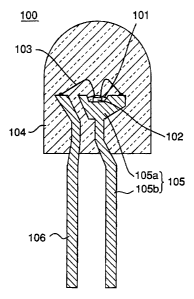
A light emitting diode 100 of Fig. 1 is a lead type
light emitting diode having a mount lead 105 and an inner lead
106, wherein a light emitting component 102 is installed on a
cup 105a of the mount lead 105, and the cup 105a is filled
with a coating resin 101 which contains a specified phosphor
to cover the light emitting component 102 and is molded in
resin. An n electrode and a p electrode of the light emitting
component 102 are connected to the mount lead 105 and the
inner lead 106, respectively, by means of wires 103.
In the light emitting diode constituted as described
above, part of light emitted by the light emitting component
(LED chip) 102 (hereinafter referred to as LED light) excites
the phosphor contained in the coating resin 101 to generate
fluorescent light having a wavelength different from that of
19
CA 02479842 2004-09-28
LED light, so that the fluorescent light emitted by the
phosphor and LED light which is output without contributing to
the excitation of the phosphor are mixed and output. As a
result, the light emitting diode 100 also outputs light having
a wavelength different from that of LED light emitted by the
light emitting component 102.
Fig. 2 shows a chip type light emitting diode,
wherein light emitting diode (LED chip) 202 is installed in a
recess of a casing 204 which is filled with a coating material
which contains a specified phosphor to form a coating 201.
The light emitting component 202 is fixed by using an epoxy
resin or the like which contains Ag, for example, and an n
electrode and a p electrode of the light emitting component
202 are connected to metal terminals 205 installed on the
casing 204 by means of conductive wires 203. In the chip type
light emitting diode constituted as described above, similarly
to the lead type light emitting diode of Fig. 1, fluorescent
light emitted by the phosphor and LED light which is
transmitted without being absorbed by the phosphor are mixed
and output, so that the light emitting diode 200 also outputs
light having a wavelength different from that of LED light
emitted by the light emitting component 202.
The light emitting diode containing the phosphor as
described above has the following features.
1. Light emitted by a light emitting component
(LED) is usually emitted through an electrode which supplies
CA 02479842 2004-09-28
electric power to the light emitting component. Emitted light
is partly blocked by the electrode formed on the light
emitting component resulting in a particular emission pattern,
and is therefore not emitted uniformly in every direction.
The light emitting diode which contains the fluorescent
material, however, can emit light uniformly over a wide range
without forming undesirable emission pattern because the light
is emitted after being diffused by the fluorescent material.
2. Although light emitted by the light emitting
component (LED) has a monochromatic peak, the peak is broad
and has high color rendering property. This characteristic
makes an indispensable advantage for an application which
requires wavelengths of a relatively wide range. Light source
for an optical image scanner, for example, is desirable to
have a wider emission peak.
The light emitting diodes of the first and second
embodiments to be described below have the configuration shown
in Fig. 1 or Fig. 2 wherein a light emitting component which
uses nitride compound semiconductor having relatively high
energy in the visible region and a particular phosphor are
combined, and have favorable properties such as capability to
emit light of high luminance and less degradation of light
emission efficiency and less color shift over an extended
period of use.
In general, a fluorescent material which absorbs
light of a short wavelength and emits light of a long
21
CA 02479842 2004-09-28
wavelength has higher efficiency than a fluorescent material
which absorbs light of a long wavelength and emits light of a
short wavelength, and therefore it is preferable to use a
nitride compound semiconductor light emitting component which
is capable of emitting blue light of short wavelength. It
needs not to be said that the use of a light emitting
component having high luminance is preferable.
A phosphor to be used in combination with the
nitride compound semiconductor light emitting component must
have the following requirements:
1. Excellent resistance against light to endure
light of a high intensity for a long period of time, because
the fluorescent material is installed in the vicinity of the
light emitting components 102, 202 and is exposed to light of
intensity as high as about 30 to 40 times that of sun light.
2. Capability to efficiently emit light in blue
region for the excitation by means of the light emitting
components 102, 202. When mixing of colors is used, should be
capable of emitting blue light, not ultraviolet ray, with a
high efficiency.
3. Capability to emit light from green to red
regions for the purpose of mixing with blue light to generate
white light.
4. Good temperature characteristic suitable for
location in the vicinity of the light emitting components 102,
202 and the resultant influence of temperature difference due
22
CA 02479842 2004-09-28
to heat generated by the chip when lighting.
5. Capability to continuously change the color tone
in terms of the proportion of composition or ratio of mixing a
plurality of fluorescent materials.
6. Weatherability for the operating environment of
the light emitting diode.
Embodiment 1
The light emitting diode of the first embodiment of
the present invention employs a gallium nitride compound
semiconductor element which has high-energy band gap in the
light emitting layer and is capable of emitting blue light,
and a garnet phosphor activated with cerium in combination.
With this configuration, the light emitting diode of the first
embodiment can emit white light by blending blue light emitted
by the light emitting components 102, 202 and yellow light
emitted by the phosphor excited by the blue light.
Because the garnet phosphor activated with cerium
which is used in the light emitting diode of the first
embodiment has light resistance and weatherability, it can
emit light with extremely small degrees of color shift and
decrease in the luminance of emitted light even when
irradiated by very intense light emitted by the light emitting
components 102, 202 located in the vicinity over a long period
of time.
Components of the light emitting diode of the first
embodiment will be described in detail below.
23
CA 02479842 2004-09-28
(Phosphor)
The phosphor used in the light emitting diode of the
first embodiment is a phosphor which, when excited by visible
light or ultraviolet ray emitted by the semiconductor light
emitting layer, emits light of a wavelength different from
that of the exciting light. The phosphor is specifically
garnet fluorescent material activated with cerium which
contains at least one element selected from Y. Lu, Sc, La, Gd
and Sm and at least one element selected from Al, Ga and In.
According to the present invention, the fluorescent material
is preferably yttrium-aluminum-garnet fluorescent material
(YAG phosphor) activated with cerium, or a fluorescent
material represented by general formula (Re,_.Sm=)3(Al,_
=Gae) 5012 : Ce, where 0sr<1 and 0sss1, and Re is at least one
selected from Y and Gd. In case the LED light emitted by the
light emitting component employing the gallium nitride
compound semiconductor and the fluorescent light emitted by
the phosphor having yellow body color are in the relation of
complementary colors, white color can be the output by
blending the LED light and the fluorescent light.
In the first embodiment, because the phosphor is
blended with a resin in use to make the coating resin 101
and the coating material 201 (detailed later), color tone of
the light emitting diode can be adjusted to include white
and incandescent lamp color by controlling the mixing
proportion with the resin or the quantity used in filling the
24
CA 02479842 2004-09-28
cup 105 or the recess of the casing 204 in accordance to the
wavelength of light emitted by the gallium nitride light
emitting component.
Distribution of the phosphor concentration has
influence also on the color blending and durability. That is,
when the concentration of phosphor increases from the surface
of the coating or molding where the phosphor is contained
toward the light emitting component, it becomes less likely to
be affected by extraneous moisture thereby making it easier to
suppress deterioration due to moisture. On the other hand,
when the concentration of phosphor increases from the light
emitting component toward the surface of the molding, it
becomes more likely to be affected by extraneous moisture, but
less likely to be affected by the heat and radiation from the
light emitting component, thus making it possible to suppress
the deterioration of the phosphor. Such distributions of the
phosphor concentration can be achieved by selecting or
controlling the material which contains the phosphor, forming
temperature and viscosity, and the configuration and particle
distribution of the phosphor.
By using the phosphor of the first embodiment, light
emitting diode having excellent emission characteristics can
be made, because the fluorescent material has enough light
resistance for high-efficient operation even when arranged
adjacent to or in the vicinity of the light emitting
components 102, 202 with radiation intensity
CA 02479842 2004-09-28
(Ee) within the range from 3 Wcm`2 to 10 Wcm-2.
The phosphor used in the first embodiment is,
because of garnet structure, resistant to heat, light and
moisture, and is therefore capable of absorbing excitation
light having a peak at a wavelength near 450 nm as shown in
Fig. 3A. It also emits broad spectrum light having a peak
near 580 nm tailing out to 700 rim as shown in Fig. 3B.
Moreover, the efficiency of excited light emission in a region
of wavelengths 460 nm and higher can be increased by including
Gd in the crystal of the phosphor of the first embodiment. When
the Gd content is increased, emission peak wavelength is
shifted toward longer wavelength and the entire emission
spectrum is shifted toward longer wavelengths. This means
that, when emission of more reddish light is required, it can
be achieved by increasing the degree of substitution with Gd.
When the Gd content is increased, luminance of light emitted
by photoluminescence under blue light tends to decrease.
Especially when part of Al is substituted with Ga
among the composition of YAG fluorescent material having
garnet structure, wavelength of emitted light shifts toward
shorter wavelength and, when part of Y is substituted with Gd,
wavelength of emitted light shifts toward longer wavelength.
Table 1 shows the composition and light emitting
characteristics of YAG fluorescent material represented by
general formula (Yl_,Gda)3(All_bGab)5O12:Ce.
26
CA 02479842 2004-09-28
U
00 M M
'v o o r-I r-i D
co
7-4 4-1
4-
4)
U
>+ 0 V 0 rn N
~O d' M N 9-1 0
.rq w tf= N Ln Ln I
U U O o 0 0 0 0 o
.rq
b
N
0 r-1 N On In N CT1 O
O pC eN M N -0 to
U
W O O 0 0 0 0 0
H
U
.0
4J
N rd
+-)
C3 O eM Lf1 O 0 O O
.
Q }4 . = = = . O.
U cd o O O O O O
O
0
+-) ~ td
41 o O O N kO 00
O p .
U to o O O o 0 0 0
r-r-I
G) =
r-) 0 N cn dv Ln %0 N
A z
b
H
27
CA 02479842 2004-09-28
values shown in Table 1 were measured by exciting
the fluorescent material with blue light of 460nm. Luminance
and efficiency in Table 1 are given in values relative to
those of material No. 1 which are set to 100.
When substituting Al with Ga, the proportion is
preferably within the range from Ga:Al=1:1 to 4:6 in
consideration of the emission efficiency and emission
wavelength. Similarly, when substituting Y with Gd, the
proportion is preferably within the range from Y:Gd=9:1 to
1:9, and more preferably from 4:1 to 2:3. It is because a
degree of substitution with Gd below 20% results in a color of
greater green component and less red component, and a degree
of substitution with Gd above 60% results in increased red
component but rapid decrease in luminance. When the ratio
Y:Gd of Y and Gd in the YAG fluorescent material is set within
the range from 4:1 to 2:3, in particular, a light emitting
diode capable of emitting white light substantially along the
black body radiation locus can be made by using one kind of
yttrium-aluminum-garnet fluorescent material, depending on the
emission wavelength of the light emitting component. When the
ratio Y:Gd of Y and Gd in the YAG fluorescent material is set
within the range from 2:3 to 1:4, a light emitting diode
capable of emitting light of incandescent lamp can be made
though the luminance is low. When the content (degree of
substitution) of Ce is set within the range from 0.003 to 0.2,
the relative luminous intensity of light emitting diode of not
28
CA 02479842 2004-09-28
less than 70% can be achieved. When the content is less than
0.003, luminous intensity decreases because the number of
excited emission centers of photoluminescence due to Ce
decreases and, when the content is greater than 0.2, density
quenching occurs.
Thus the wavelength of the emitted light can be
shifted to a shorter wavelength by substituting part of Al of
the composition with Ga, and the wavelength of the emitted
light can be shifted to a longer wavelength by substituting
part of Y of the composition with Gd. In this way, the light
color of emission can be changed continuously by changing the
composition. Also the fluorescent material is hardly excited
by Hg emission lines which have such wavelengths as 254 nm and
365 nm, but is excited with higher efficiency by LED light
emitted by a blue light emitting component having a wavelength
around 450 nm. Thus the fluorescent material has ideal
characteristics for converting blue light of nitride
semiconductor light emitting component into white light, such
as the capability of continuously changing the peak wavelength
by-changing the proportion of Gd.
According to the first embodiment, the efficiency of
light emission of the light emitting diode can be further
improved by combining the light emitting component employing
gallium nitride semiconductor and the phosphor made by adding
rare earth element samarium (Sm) to yttrium-aluminum-garnet
fluorescent materials (YAG) activated with cerium.
29
CA 02479842 2004-09-28
Material for making such a phosphor is made by using
oxides of Y, Gd, Ce, Sm, Al and Ga or compounds which can be
easily converted into these oxides at high temperature, and
sufficiently mixing these materials in stoichiometrical
proportions. This mixture is mixed with an appropriate
quantity of a fluoride such as ammonium fluoride used as a
flux, and fired in a crucible at a temperature from 1350 to
1450 C in air for 2 to 5 hours. Then the fired material is
ground by a ball mill in water, washed, separated, dried and
sieved thereby to obtain the desired material.
In the producing process described above, the
mixture material may also be made by dissolving rare earth
elements Y, Gd, Ce and Sm in stoichiometrical proportions in
an acid, coprecipitating the solution with oxalic acid and
firing the coprecipitate to obtain an oxide of the
coprecipitate, and then mixing it with aluminum oxide and
gallium oxide.
The phosphor represented by the general formula (Y1_
P_4_rGdpCe9Smr)3A1,012 can emit light of wavelengths 460nm and
longer with higher efficiency upon excitation, because Gd is
contained in the crystal. When the content of gadolinium is
increased, peak wavelength of emission shifts from 530nm to a
longer wavelength up to 570nm, while the entire emission
spectrum also shifts to longer wavelengths. When light of
stronger red shade is needed, it can be achieved by increasing
the amount of Gd added for substitution. When the content of
CA 02479842 2004-09-28
Gd is increased, luminance of photoluminescence with blue
light gradually decreases. Therefore, value of p is
preferably 0.8 or lower, or more preferably 0.7 or lower.
Further more preferably it is 0.6 or lower.
The phosphor represented by the general formula (Y1_
p_q_rGdpCegSmr)3A15O12 including Sm can be made subject to less
dependence on temperature regardless of the increased content
of Gd. That is, the phosphor, when Sm is contained, has
greatly improved emission luminance at higher temperatures.
Extent of the improvement increases as the Gd content is
increased. Temperature characteristic can be greatly improved
particularly by the addition of Sm in the case of fluorescent
material of such a composition as red shade is strengthened by
increasing the content of Gd, because it has poor temperature
characteristics. The temperature characteristic mentioned
here is measured in terms of the ratio ($) of emission
luminance of the fluorescent material at a high temperature
(200 C) relative to the emission luminance of exciting blue
light having a wavelength of 450nm at the normal temperature
(25-C).
The proportion of Sm is preferably within the range
of 0.0003srs0.08 to give temperature characteristic of 60% or
higher. The value of r below this range leads to less effect
of improving the temperature characteristic. When the value
of r is above this range, on the contrary, the temperature
characteristic deteriorates. The range of 0.0007srs0.02 for
31
CA 02479842 2004-09-28
the proportion of Sm where temperature characteristic becomes
80% or higher is more desirable.
The proportion q of Ce is preferably in a range of
0.003sgs0.2, which makes relative emission luminance of 70% or
higher possible. The relative emission luminance refers to
the emission luminance in terms of percentage to the emission
luminance of a fluorescent material where q=0.03.
When the proportion q of Ce is 0.003 or lower,
luminance decreases because the number of excited emission
centers of photoluminescence due to Ce decreases and, when the
q is greater than 0.2, density quenching occurs. Density
quenching refers to the decrease in emission intensity which
occurs when the concentration of an activation agent added to
increase the luminance of the fluorescent material is
increased beyond an optimum level.
For the light emitting diode of the present
invention, a mixture of two or more kinds of phosphors having
compositions of (Y1_p_g_rGdpCegSmr) 3Al5o12 having different contents
of Al, Ga, Y and Gs or Sm may also be used. This increases
the RGB components and enables the application, for example,
for a full-color liquid crystal display device by using a
color filter.
(Light emitting components 102, 202)
The light emitting component is preferably embedded
in a molding material as shown in Fig. 1 and Fig. 2. The
light emitting component used in the light emitting diode of
32
CA 02479842 2004-09-28
the present invention is a gallium nitride compound
semiconductor capable of efficiently exciting the garnet
fluorescent materials activated with cerium. The light
emitting components 102, 202 employing gallium nitride
compound semiconductor are made by forming a light emitting
layer of gallium nitride semiconductor such as InGaN on a
substrate in the MOCVD process. The structure of the light
emitting component may be homostructure, heterostructure or
double-heterostructure which have MIS junction, PIN junction
or PN junction. Various wavelengths of emission can be
selected depending on the material of the semiconductor layer
and the crystallinity thereof. It may also be made in a
single quantum well structure or multiple quantum well
structure where a semiconductor activation layer is formed as
thin as quantum effect can occur. According to the present
invention, a light emitting diode capable of emitting with
higher luminance without deterioration of the phosphor can be
made by making the activation layer of the light emitting
component in single quantum well structure of InGaN.
When a gallium nitride compound semiconductor is
used, while sapphire, spinnel, SiC, Si, ZnO or the like may be
used as the semiconductor substrate, use of sapphire substrate
is preferable in order to form gallium nitride of good
crystallinity. A gallium nitride semiconductor layer is
formed on the sapphire substrate to form a PN junction via a
buffer layer of GaN, A1N, etc. The gallium nitride
33
CA 02479842 2004-09-28
semiconductor has N type conductivity under the conditions
of no impurity doping, although in order to form an N
type gallium nitride semiconductor having desired properties
(carrier concentration, etc.) such as improved light emission
efficiency, it is preferably doped with N type dopant such as
Si, Ge, Se, Te, and C. In order to form a P type gallium
nitride semiconductor, on the other hand, it is preferably
doped with P type dopant such as Zn, Mg, Be, Ca, Sr and Ba.
Because it is difficult to turn a gallium nitride compound
semiconductor to P type simply by doping a P type dopant, it
is preferable to treat the gallium nitride compound
semiconductor doped with P type dopant in such process as
heating in a furnace, irradiation with low-speed electron beam
and plasma irradiation, thereby to turn it to P type.. After
exposing the surfaces of P type and N type gallium nitride
semiconductors by the etching or other process, electrodes of
the desired shapes are formed on the semiconductor layers by
sputtering or vapor deposition.
Then the semiconductor wafer which has been formed
is cut into pieces by means of a dicing saw, or separated by
an external force after cutting grooves (half-cut) which have
width greater than the blade edge width. Or otherwise, the
wafer is cut into chips by scribing grid pattern of extremely
fine lines on the semiconductor wafer by means of a scriber
having a diamond stylus which makes straight reciprocal
movement. Thus the light emitting component of gallium
34
CA 02479842 2004-09-28
nitride compound semiconductor can be made.
In order to emit white light with the light emitting
diode of the f irst embodiment, wavelength of light emitted by
the light emitting component is preferably from 400nm to 530nm
inclusive in consideration of the complementary color
relationship with the phosphor and deterioration of resin, and
more preferably from 420nm to 490nm inclusive. It is further
more preferable that the wavelength be from 450nm to 475nm, in
order to improve the emission efficiency of the light emitting
component and the phosphor. Emission spectrum of the white
light emitting diode of the first embodiment is shown in Fig.
4. The light emitting component shown here is of lead type
shown in Fig. 1, which employs the light emitting component
and the phosphor of the first embodiment to be described later.
In Fig. 4, emission having a peak around 450 nm is the light
emitted by the light emitting component, and emission having a
peak around 570 nm is the photoluminescent emission excited by
the light emitting component.
Fig. 16 shows the colors which can be represented by
the white light emitting diode made by combining the
fluorescent material shown in Table 1 and blue LED (light
emitting component) having peak wavelength 465nm. Color of
light emitted by this white light emitting diode corresponds
to a point on a straight line connecting a point of
chromaticity generated by the blue LED and a point of
chromaticity generated by the fluorescent material, and
CA 02479842 2004-09-28
therefore the wide white color region (shaded portion in Fig.
16) in the central portion of the chromaticity diagram can be
fully covered by using the fluorescent materials 1 to 7 in
Table 1. Fig. 17 shows the change in emission color when the
contents of fluorescent materials in the white light emitting
diode is changed. Contents of fluorescent materials are given
in weight percentage to the resin used in the coating material.
As will be seen from Fig. 17, color of the light approaches
that of the fluorescent materials when the content of
fluorescent material is increased and approaches that of blue
LED when the content of fluorescent material decreases.
According to the present invention, a light emitting
component which does not excite the fluorescent material may
be used together with the light emitting component which emits
light that excites the fluorescent material. Specifically, in
addition to the fluorescent material which is a nitride
compound semiconductor capable of exciting the fluorescent
material, a light emitting component having a light emitting
layer made of gallium phosphate, gallium aluminum arsenide,
gallium arsenic phosphate or indium aluminum phosphate is
arranged together. With this configuration, light emitted by
the light emitting component which does not excite the
fluorescent material is radiated to the outside without being
absorbed by the fluorescent material, making a light emitting
diode which can emit red/white light.
Other components of the light emitting diodes of Fig.
36
CA 02479842 2004-09-28
1 and Fig. 2 will be described below.
(Conductive wires 103, 203)
The conductive wires 103, 203 should have good
electric conductivity, good thermal conductivity and good
mechanical connection with the electrodes of the light
emitting components 102, 202. Thermal conductivity is
preferably 0.01 cal/(s)(cm2)( C/cm) or higher, and more
preferably 0.5 cal/(s)(cm2)( C/cm) or higher. For workability,
diameter of the conductive wire is preferably from 10pm to
45pm inclusive. Even when the same material is used for both
the coating including the fluorescent material and the molding,
because of the difference in thermal expansion coefficient due
to the fluorescent material contained in either of the above
two materials, the conductive wire is likely to break at the
interface. For this reason, diameter of the conductive wire
is preferably not less than 25pm and, for the reason of light
emitting area and ease of handling, preferably within 35pm.
The conductive wire may be a metal such as gold, copper,
platinum and aluminum or an alloy thereof. When a conductive
wire of such material and configuration is used, it can be
easily connected to the electrodes of the light emitting
components, the inner lead and the mount lead by means of a
wire bonding device.
(Mount lead 105)
The mount lead 105 comprises a cup 105a and a lead
105b, and it suffices to have a size enough for mounting the
37
CA 02479842 2004-09-28
light emitting component 102 with the wire bonding device in
the cup 105a. 'In case a plurality of light emitting
components are installed in the cup and the mount lead is used
as common electrode for the light emitting component, because
different electrode materials may be used, sufficient
electrical conductivity and good conductivity with the bonding
wire and others are required. When the light emitting
component is installed in the cup of the mount lead and the
cup is filled with the fluorescent material, light emitted by
the fluorescent material is, even if isotropic, reflected by
the cup in a desired direction and therefore erroneous
illumination due to light from another light emitting diode
mounted nearby can be prevented. Erroneous illumination here
refers to a phenomenon such as another light emitting diode
mounted nearby appearing as though lighting despite not being
supplied with power.
Bonding of the light emitting component 102 and the
mount lead 105 with the cup 105a can be achieved by means of a
thermoplastic resin such as epoxy resin, acrylic resin and
imide resin. When a face-down light emitting component
(a type of light emitting component such as emitted light is
extracted from the substrate side and is configured for
mounting the electrodes to oppose the cup 105a) is used, Ag
paste, carbon paste, metallic bump or the like can be used for
bonding and electrically connecting the light emitting
component and the mount lead at the same time. Further, in
38
CA 02479842 2004-09-28
order to improve the efficiency of light utilization of the
light emitting diode, surface of the cup of the mount lead
whereon the light emitting component is mounted may be mirror-
polished to give a reflecting function to the surface. In this
case, the surface roughness is preferably from O.1S to 0.8 S
inclusive. Electric resistance of the mount lead is
preferably within 300pQ.=cm and more preferably within 3pQ.=cm..
When mounting a plurality of light emitting components on the
mount lead, the light emitting components generate a significant
amount of heat and therefore high thermal conductivity is
required. Specifically, the thermal conductivity is
preferably 0.01 cal/(s)(cm2)( C/cm) or higher, and more
preferably 0.5 cal/ (s) (cm2) ( C/cm) or higher. Materials which
satisfy these requirements contain steel, copper, copper-clad
steel, copper-clad tin and metallized ceramics.
(Inner lead 106)
The inner lead 106 is connected to one of the electrodes
of the light emitting component 102 mounted on the mount lead
105 by means of conductive wire or the like. In the case of a
light emitting diode where a plurality of the light emitting
components are installed on the mount lead, it is necessary to
arrange a plurality of inner leads 106 in such a manner that
the conductive wires do not touch each other. For example,
contact of the conductive wires with each other can be
prevented by increasing the area of the end face where the
inner lead is wire-bonded as the distance from the mount lead
39
CA 02479842 2004-09-28
increases so that the space between the conductive wires is
secured. Surface roughness of the inner lead end face
connecting with the conductive wire is preferably from 1.6 S
to 10 S inclusive in consideration of close contact.
In order to form the inner lead in a desired shape, it
may be punched by means of a die. Further, it may be made by
punching to form the inner lead then pressurizing it on the
end face thereby to control the area and height of the end
face.
The inner lead is required to have good connectivity
with the bonding wires which are conductive wires and have
good electrical conductivity. Specifically, the electric
resistance is preferably within 300pQ.=cm and more preferably
within 3pQ.=cm. Materials which satisfy these requirements
contain iron, copper, iron-containing copper, tin-containing
copper, copper-, gold- or silver-plated aluminum, iron and
copper.
(Coating material 101)
The coating material 101 is provided in the cup of
the mount lead apart from the molding material 104 and, in the
first embodiment, contains the phosphor which converts the
light emitted by the light emitting component. The coating
material may be a transparent material having good
weatherability such as epoxy resin, urea resin and silicone or
glass. A dispersant may be used together with the phosphor.
As the dispersant, barium titanate, titanium oxide, aluminum
CA 02479842 2004-09-28
oxide, silicon dioxide and the like are preferably used. When
the fluorescent material is formed by sputtering, coating
material may be omitted. In this case, a light emitting diode
capable of bending colors can be made by controlling the film
thickness or providing an aperture in the fluorescent material
layer.
(Molding material 104)
The molding material 104 has the function to protect the
light emitting component 102, the conductive wire 103 and the
coating material 101 which contains phosphor from external
disturbance. According to the first embodiment, it is
preferable that the molding material 104 further contain a
dispersant, which can unsharpen the directivity of light from
the light emitting component 102, resulting in increased angle
of view. The molding material 104 has the function of lens to
focus or diffuse the light emitted by the light emitting
component. Therefore, the molding material 104 may be made in
a configuration of convex lens or concave lens, and may have
an elliptic shape when viewed in the direction of optical axis,
or a combination of these. Also the molding material 104 may
be made in a structure of multiple layers of different
materials being laminated. As the molding material 104,
transparent materials having high weatherability such as epoxy
resin, urea resin, silicon resin or glass is preferably
employed. As the dispersant, barium titanate, titanium oxide,
aluminum oxide, silicon dioxide and the like can be used. In
41
CA 02479842 2004-09-28
addition to the dispersant, phosphor may also be contained in
the molding material. Namely, according to the present
invention, the phosphor may be contained either in the molding
material or in the coating material. When the phosphor is
contained in the molding material, angle of view can be
further increased. The phosphor may also be contained in both
the coating material and the molding material. Further, a
resin including the phosphor may be used as the coating
material while using glass, different from the coating
material, as the molding material. This makes it possible to
manufacture a light emitting diode which is less subject to
the influence of moisture with good productivity. The molding
and the coating may also be made of the same material in order
to match the refractive index, depending on the application.
According to the present invention, adding the dispersant
and/or a coloration agent in the molding material has the
effects of masking the color of the fluorescent material
obscured and improving the color mixing performance. That is,
the fluorescent material absorbs blue component of extraneous
light and emits light thereby to give such an appearance as
though colored in yellow. However, the dispersant contained
in the molding material gives milky white color to the molding
material and the coloration agent renders a desired color.
Thus the color of the fluorescent material will not be
recognized by the observer. In the case where the light
emitting component emits light having a main wavelength of
42
CA 02479842 2004-09-28
430nm or over, it is more preferable that an ultraviolet
absorber which serves as a light stabilizer be included.
Embodiment 2
The light emitting diode of the second embodiment of
the present invention is made by using an element provided
with gallium nitride compound semiconductor which has high-
energy band gap in the light emitting layer as the light
emitting component and a fluorescent material including two or
more kinds of phosphors of different compositions, or
preferably yttrium-aluminum-garnet fluorescent materials
activated with cerium as the phosphor. With this
configuration, a light emitting diode which allows a
desired color tone by controlling the contents of the two or
more fluorescent materials can be made even when the
wavelength of the LED light emitted by the light emitting
component deviates from the desired value due to variations in
the production process. In this case, emission color of the
light emitting diode can be made constant using a
fluorescent material having a relatively short emission
wavelength for a light emitting component of a relatively
short emission wavelength and using a fluorescent material
having a relatively long emission wavelength for a light
emitting component of a relatively long emission wavelength.
As for the fluorescent material, a fluorescent
material represented by general formula (Rel_rSmr) 3 (All_
.Ga.) 5012: Ce may also be used as the phosphor. Here Osr<1 and
43
CA 02479842 2004-09-28
0sss1, and Re is at least one selected from Y, Gd and La.
This configuration makes it possible to minimize the
denaturing of the fluorescent material even when the
fluorescent material is exposed to high-intensity high-energy
visible light emitted by the light emitting component for a
long period of time or when used under various environmental
conditions, and therefore a light emitting diode which is
subject to extremely insignificant color shift and emission
luminance decrease and has the desired emission component of
high luminance can be made.
(Phosphor of the second embodiment)
Now the phosphor used in the light emitting
component of the second embodiment will be described in detail
below. The second embodiment is similar to the first
embodiment, except that two or more kinds of phosphors of
different compositions activated with cerium are used as the
phosphor, as described above, and the method of using the
fluorescent material is basically the same.
Similar to the first embodiment, the light
emitting diode can be given high weatherability by
controlling the distribution of the phosphor (such as tapering
the concentration with the distance from the light emitting
component). Such a distribution of the phosphor concentration
can be achieved by selecting or controlling the material which
contains the phosphor, forming temperature and viscosity, and
the configuration and particle distribution of the phosphor.
44
CA 02479842 2004-09-28
Thus according to the second embodiment, distribution of the
fluorescent material concentration is determined according to
the operating conditions. Also according to the second
embodiment, efficiency of light emission can be increased by
designing the arrangement of the two or more kinds of
fluorescent materials (for example, arranging in the order of
nearness to the light emitting component) according to the
light generated by the light emitting component.
With the configuration of the second embodiment,
similarly to the first embodiment, light emitting diode has
high efficiency and enough light resistance even when arranged
adjacent to or in the vicinity of relatively high-output light
emitting component with radiation intensity (Ee) within the
range from 3 Wcm2 to 10 Wcm2 can be made.
The yttrium-aluminum-garnet fluorescent material.
activated with cerium (YAG fluorescent material) used in the
second embodiment has garnet structure similarly to the case
of the first embodiment, and is therefore resistant to heat,
light and moisture. The peak wavelength of excitation of the
yttrium-aluminum-garnet fluorescent material of the second
embodiment can be set near 450nm as indicated by the solid
line in Fig. 5A, and the peak wavelength of emission can be
set near 510nm as indicated by the solid line in Fig. 5B,
while making the emission spectrum so broad as to tail out to
700nm. This makes it possible to emit green light. The peak
wavelength of excitation of another yttrium-aluminum-garnet
CA 02479842 2004-09-28
fluorescent material activated with cerium of the second
embodiment can be' set near 450nm as indicated by the dashed
line in Fig. 5A, and the peak wavelength of emission can be
set near 600nm as indicated by the dashed line in Fig. 5B,
while making the emission spectrum so broad as to tail out to
750nm. This makes it possible to emit red light.
Wavelength of the emitted light is shifted to a
shorter wavelength by substituting part of Al, among the
constituents of the YAG fluorescent material having garnet
structure, with Ga, and the wavelength of the emitted light is
shifted to a longer wavelength by substituting part of Y with
Gd and/or La. Proportion of substituting Al with Ga is
preferably from Ga:Al=1:1 to 4:6 in consideration of the light
emitting efficiency and the wavelength of emission. Similarly,
proportion of substituting Y with Gd and/or La is preferably
from Y:Gd and/or La=9:1 to 1:9, or more preferably from Y:Gd
and/or La=4:1 to 2:3. Substitution of less than 20% results
in an increase of green component and a decrease of red
component. Substitution of 80% or greater part, on the other
hand, increases red component but decreases the luminance
steeply.
Material for making such a phosphor is made by using
oxides of Y, Gd, Ce, La, Al, Sm and Ga or compounds which can
be easily converted into these oxides at high temperature, and
sufficiently mixing these materials in stoichiometrical
proportions. Alternatively, the mixture material is obtained by
46
CA 02479842 2004-09-28
dissolving rare earth elements Y, Gd, Ce, La and Sm in
stoichiometrical proportions in acid, coprecipitating the
solution oxalic acid and firing the coprecipitate to obtain an
oxide of the coprecipitate, which is then mixed with aluminum
oxide and gallium oxide. This mixture is mixed with an
appropriate quantity of a fluoride such as ammonium fluoride
used as a flux, and fired in a crucible at a temperature from
1350 to 1450 C in air for 2 to 5 hours. Then the fired
material is ground by a ball mill in water, washed, separated,
dried and sieved thereby to obtain the desired material.
In the second embodiment, the two or more kinds of
yttrium-aluminum-garnet fluorescent materials activated with
cerium of different compositions may be either used by mixing
or arranged independently (laminated, for example). When the
two or more kinds of fluorescent materials are mixed, color
converting portion can be formed relatively easily and in a
manner suitable for mass production. When the two or more
kinds of fluorescent materials are arranged independently,
color can be adjusted after forming it by laminating the
layers until a desired color can be obtained. Also when
arranging the two or more kinds of fluorescent materials
independently, it is preferable to arrange a fluorescent
material that absorbs light from the light emitting component
of a shorter wavelength near to the LED element, and a
fluorescent material that absorbs light of a longer wavelength
away from the LED element. This arrangement enables efficient
47
CA 02479842 2004-09-28
absorption and emission of light.
The light emitting diode of the second embodiment is
made by using two or more kinds of yttrium-aluminum-garnet
fluorescent materials of different compositions as the
fluorescent materials, as described above. This makes it
possible to make a light emitting diode capable of emitting
light of desired color efficiently. That is, when wavelength
of light emitted by the semiconductor light emitting component
corresponds to a point on the straight line connecting point A
and point B in the chromaticity diagram of Fig. 6, light of
any color in the shaded region enclosed by points A, B, C and
D in Fig. 6 which is the chromaticity points (points C and D)
of the two or more kinds of yttrium-aluminum-garnet
fluorescent materials of different compositions can be emitted.
According to the second embodiment, color can be controlled by
changing the compositions or quantities of the LED elements
and fluorescent materials. In particular, a light emitting
diode of less variation in the emission wavelength can be made
by selecting the fluorescent materials according to the
emission wavelength of the LED element, thereby compensating
for the variation of the emission wavelength of the LED
element. Also a light emitting diode including RGB components
with high luminance can be made by selecting the emission
wavelength of the fluorescent materials.
25, Moreover, because the yttrium-aluminum-garnet (YAG)
fluorescent material used in the second embodiment has garnet
48
CA 02479842 2004-09-28
structure, the light emitting diode of the second embodiment
can emit light of high luminance for a long period of time.
Also the light emitting diodes of the first embodiment and the
second embodiment are provided with a light emitting component
installed via fluorescent material. Also because the
converted light has longer wavelength than that of the light
emitted by the light emitting component, energy of the
converted light is less than the band gap of the nitride
semiconductor, and is less likely to be absorbed by the
nitride semiconductor layer. Thus, although the light emitted
by the fluorescent material is directed also to the LED
element because of the isotropy of emission, the light emitted
by the fluorescent material is never absorbed by the LED
element, and therefore the emission efficiency of the light
emitting diode will not be decreased.
(Planar light source)
A planar light source which is another embodiment of
the present invention is shown in Fig. 7.
In the planar light source shown in the Fig. 7, the
phosphor used in the first embodiment or the second embodiment
is contained in a coating material 701. With this
configuration, blue light emitted by the gallium nitride
semiconductor is color-converted and is output in planar state
via an optical guide plate 704 and a dispersive sheet 706.
Specifically, a light emitting component 702 of the
planar light source of Fig. 7 is secured in a metal substrate
49
CA 02479842 2004-09-28
703 of inverted C shape whereon an insulation layer and a
conductive pattern (not shown) are formed. After electrically
connecting the electrode of the light emitting component and
the conductive pattern, phosphor is mixed with epoxy resin and
applied into the inverse C-shaped metal substrate 703 whereon
the light emitting component 702 is mounted. The light
emitting component thus secured is fixed onto an end face of
an acrylic optical guide plate 704 by means of an epoxy resin.
A reflector film 707 containing a white diffusion agent is
arranged on one of principal planes of the optical guide plate
704 where the dispersive sheet 706 is not formed, for the
purpose of preventing fluorescence.
Similarly, a reflector 705 is provided on the entire
surface on the back of the optical guide plate 704 and on one
end face where the light emitting component is not provided,,
in order to improve the light emission efficiency. With this
configuration, light emitting diodes for planar light emission
which generates enough luminance for the back light of LCD can
be made.
Application of the light emitting diode for planar
light emission to a liquid crystal display can be achieved by
arranging a polarizer plate on one principal plane of the
optical guide plate 704 via liquid crystal injected between
glass substrates (not shown) whereon a translucent conductive
pattern is formed.
Now referring to Fig. 8 and Fig. 9, a planar light
CA 02479842 2004-09-28
source according to another embodiment of the present
invention will be described below. The light emitting device
shown in Fig. 8 is made in such a configuration that blue
light emitted by the light emitting diode 702 is converted to
white light by a color converter 701 which contains phosphor
and is output in planar state via an optical guide plate 704.
The light emitting device shown in Fig. 9 is made in
such a configuration that blue light emitted by the light
emitting component 702 is turned to planar state by the
optical guide plate 704, then converted to white light by a
dispersive sheet 706 which contains phosphor formed on one of
the principal planes of the optical guide plate 704, thereby to
output white light in a planar state. The phosphor may be
either contained in the dispersive sheet 706 or formed in a
sheet by spreading it together with a binder resin over the
dispersive sheet 706. Further, the binder including the
phosphor may be formed as dots, not a sheet, directly on the
optical guide plate 704.
<Application>
(Display device)
Now a display device according to the present
invention will be described below. Fig. 10 is a block diagram
showing the configuration of the display device according to
the present invention. As shown in Fig. 10, the display
device comprises an LED display device 601 and a drive circuit
610 having a driver 602, video data storage means 603 and tone
51
CA 02479842 2004-09-28
control means 604. The LED display device 601, having white
light emitting diodes 501 shown in Fig. 1 or Fig. 2 arranged
in matrix configuration in a casing 504 as shown in Fig. 11,
is used as monochromatic LED display device. The casing 504
is provided with h light blocking material 505 being formed
integrally therewith.
The drive circuit 610 has the video data storage
means (RAM) 603 for temporarily storing display data which is
input, the tone control means 604 which computes and outputs
tone signals for controlling the individual light emitting
diodes of the LED display device 601 to light with the
specified brightness according to the data read from RAM 603,
and the driver 602 which is switched by signals supplied from
the tone control means 604 to drive the light emitting diode
to light. The tone control circuit 604 retrieves data from
the RAM 603 and computes the duration of lighting the light
emitting diodes of the LED display device 601, then outputs
pulse signals for turning on and off the light emitting diodes
to the LED display device 601. In the display device
constituted as described above, the LED display device 601 is
capable of displaying images according to the pulse signals
which are input from the drive circuit, and has the following
advantages.
The LED display device which displays with white
light by using light emitting diodes of three colors, RGB, is
required to display while controlling the light emission
52
CA 02479842 2004-09-28
output of the R, G and B light emitting diodes and
accordingly must control the light emitting diodes by taking
the emission intensity, temperature characteristics and
other factors of the light emitting diodes into account,
resulting in complicated configuration of the drive circuit
which drives the LED display device. In the display device
of the present invention, however, because the LED display
device 601 is constituted by using light emitting diodes 501
of the present invention which can emit white light without
using light emitting diodes of three kinds, RGB, it is not
necessary for the drive circuit to individually control the
R, G and B light emitting diodes, making it possible to
simplify the configuration of the drive circuit and make the
display device at a low cost.
With an LED display device which displays in white
light by using light emitting diodes of three kinds, RGB,
the three light emitting diodes must be illuminated at the
same time and the light from the light emitting diodes must
be mixed in order to display white light by combining the
three RGB light emitting diodes for each pixel, resulting in
a large display area for each pixel and making it impossible
to display with high definition. The LED display device of
the display device according to the present invention, in
contrast, can display white light with a single light
emitting diode, and is therefore capable of display with white
53
CA 02479842 2004-09-28
light of higher definition. Further, with the LED display
device which displays by mixing the colors of three light
emitting diodes, there is such a case as the display color
changes due to blocking of some of the RGB light emitting
diodes depending on the viewing angle, the LED display device
of the present invention has no such problem.
As described above, the display device provided with
the LED display device employing the light emitting diode of
the present invention which is capable of emitting white light
is capable of displaying stable white light with higher
definition and has an advantage of less color unevenness. The
LED display device of the present invention which is capable
of displaying with white light also imposes less stimulation
to the eye compared to the conventional LED display device
which employs only red and green colors, and is therefore
suited for use over a long period of time.
(Embodiment of another display device employing the light
emitting diode of the present invention)
The light emitting diode of the present invention
can be used to constitute an LED display device wherein one
pixel is constituted of three RGB light emitting diodes and
one light emitting diode of the present invention, as shown in
Fig. 12. By connecting the LED display device and a specified
drive circuit, a display device capable of displaying various
images can be constituted. The drive circuit of this display
device has, similarly to a case of monochrome display device,
54
CA 02479842 2004-09-28
video data storage means (RAM)for temporarily storing the
input display data, a tone control circuit which processes the
data stored in the RAM to compute tone signals for lighting
the light emitting diodes with specified brightness and a
driver which is switched by the output signal of the tone
control circuit to cause the light emitting diodes to
illuminate. The drive circuit is required exclusively for
each of the RGB light emitting diodes and the white light
emitting diode. The tone control circuit computes the
duration of lighting the light emitting diodes from the data
stored in the RAM, and outputs pulse signals for turning on
and off the light emitting diodes. When displaying with white
light, width of the pulse signals for lighting the RGB light
emitting diodes is made shorter, or peak value of the pulse
signal is made lower or no pulse signal is output at all. On
the other hand, a pulse signal is given to the white light
emitting diode in compensation thereof. This causes the LED
display device to display with white light.
As described above, brightness of display can be
improved by adding the white light emitting diode to the RGB
light emitting diodes. When RGB light emitting diodes are
combined to display white light, one or two of the RGB colors
may be enhanced resulting in a failure to display pure white
depending on the viewing angle, such a problem is solved by
adding the white light emitting diode as in this display
device.
CA 02479842 2004-09-28
For the drive circuit of a display device such as that
described above, it is preferable that a CPU be provided
separately as a tone control circuit which computes the pulse
signal for lighting the white light emitting diode with
specified brightness. The pulse signal which is output from
the tone control circuit is given to the white light emitting
diode driver thereby to switch the driver. The white light
emitting diode illuminates when the driver is turned on, and
goes out when the driver is turned off.
(Traffic signal)
When the light emitting diode of the present
invention is used as a traffic signal which is a kind of
display device, advantages can be obtained such as stable
illumination over a long period of time and no color
unevenness even when part of the light emitting diodes go out.
The traffic signal employing the light emitting diode of the
present invention has a configuration such that the white light
emitting diodes are arranged on a substrate whereon a
conductive pattern is formed. A circuit of light emitting
diodes wherein such light emitting diodes are connected in
series or parallel is handled as a set of light emitting
diodes. Two or more sets of the light emitting diodes are
used, each having the light emitting diodes arranged in spiral
configuration. When all light emitting diodes are arranged,
they are arranged over the entire area in circular
configuration. After connecting power lines by soldering for
56
CA 02479842 2004-09-28
the connection of the light emitting diodes and the substrate
with external power supply, it is secured in a railway
signal chassis. The LED display device is placed in an
aluminum diecast chassis equipped with a light blocking member
and is sealed on the surface with silicon rubber filler. The
chassis is provided with a white color lens on the display
plane thereof. Electric wiring of the LED display. device is
passed through a rubber packing on the back of the chassis,
for sealing off the inside of the chassis from the outside,
with the inside of the chassis closed. Thus a white light
signal is made. A signal of higher reliability can be made by
dividing the light emitting diodes of the present invention
into a plurality of groups and arranging them in a spiral
configuration swirling from a center toward outside, while
connecting them in parallel. The configuration of swirling
from the center toward outside may be either continuous or
intermittent. Therefore, desired number of the light emitting
diodes and desired number of the sets of light emitting diodes
can be selected depending on the display area of the LED
display device. This signal is, even when one of the sets of
light emitting diodes or part of the light emitting diodes
fail to illuminate due to some trouble, capable of illuminating
evenly in a circular configuration without color shift by
means of the remaining set of light emitting diodes or
remaining light emitting diodes. Because the light emitting
diodes are arranged in a spiral configuration, they can be
57
CA 02479842 2004-09-28
arranged more densely near the center, and driven without any
different impression from signals employing incandescent lamps.
<Examples>
The following Examples further illustrate the
present invention in detail but are not to be construed to
limit the scope thereof.
(Example 1)
Example 1 provides a light emitting component having
an emission peak at 450nm and a half width of 30nm employing a
GainN semiconductor. The light emitting component of the
present invention is made by flowing TMG (trimethyl gallium)
gas, TMI (trimethyl indium) gas, nitrogen gas and dopant gas
together with a carrier gas on a cleaned sapphire substrate
and forming a gallium nitride compound semiconductor layer in
MOCVD process. A gallium nitride semiconductor having N type
conductivity and a gallium nitride semiconductor having P type
conductivity are formed by switching SiH4 and Cp2Mg as dopant
gas. The LED element of Example 1 has a contact layer which
is a gallium nitride semiconductor having N type conductivity,
a clad layer which is a gallium nitride aluminum semiconductor
having P type conductivity and a contact layer which is a
gallium nitride semiconductor having P type conductivity, and
formed between the contact layer having N type conductivity
and the clad layer having P type conductivity is a non-doped
InGAN activation layer of about 3 nm thickness for making a
single quantum well structure. The sapphire substrate has a
58
CA 02479842 2004-09-28
gallium nitride semiconductor layer formed thereon under a low
temperature to make a buffer layer. The P type semiconductor
is annealed at a temperature of 400 C or above after forming
the film.
After etching to expose the surfaces of P type and
N type semiconductor layers, n and p electrodes are formed
by sputtering. After scribing the semiconductor wafer which
has been made as described above, light emitting components
are made by dividing the wafer with external force.
The light emitting component made in the above
process is mounted in a cup of a mount lead which is made of
silver-plated steel by die bonding with epoxy resin. Then
electrodes of the light emitting component, the mount lead and
the inner lead are electrically connected by wire boding with
gold wires 30im in diameter, to make a light emitting diode of
lead type.
A phosphor is made by dissolving rare earth elements
of Y, Gd and Ce in an acid in stoichiometrical proportions,
and coprecipitating the solution with oxalic acid. Oxide of
the coprecipitate obtained by firing this material is mixed
with aluminum oxide, thereby to obtain the mixture material.
The mixture was then mixed with ammonium fluoride used as a
flux, and fired in a crucible at a temperature of 1400 C in
air for 3 hours. Then the fired material is ground by a ball
mill in water, washed, separated, dried and sieved thereby to
obtained the desired material. Phosphor made as described
59
CA 02479842 2004-09-28
above is yttrium-aluminum-garnet fluorescent material
represented by general formula (Y0 8Gd0.2 ) A15012 : Ce where about
20% of Y is substituted with Gd and substitution ratio of Ce
is 0.03.
80 Parts by weight of the fluorescent material
having a composition of (Yo.8Gdo.2) 3Al5O12 : Ce which has been made
in the above process and 100 parts by weight of epoxy resin
are mixed sufficiently to make a slurry. The slurry is
poured into the cup provided on the mount lead whereon the
light emitting component is mounted. After pouring, the
slurry is cured at 130 C for one hour. Thus a coating having
a thickness of 120pm, which contains the phosphor, is formed
on the light emitting component. In Example 1, the coating is
formed to contain the phosphor in gradually increasing
concentration toward the light emitting component.
Irradiation intensity is about 3.5W/cm2. The light emitting
component and the phosphor are molded with translucent epoxy
resin for the purpose of protection against extraneous stress,
moisture and dust. A lead frame with the coating layer of
phosphor formed thereon is placed in a bullet-shaped die and
mixed with translucent epoxy resin and then cured at 150 C
for 5 hours.
Under visual observation of the light emitting diode
formed as described above in the direction normal to the light
emitting plane, it was found that the central portion was
rendered a yellowish color due to the body color of the
phoshpor.
CA 02479842 2004-09-28
Measurements of chromaticity point, ' color
temperature and color rendering index of the light emitting
diode made as described above and capable of emitting white
light gave values of (0.302, 0.280) for chromaticity point
(x,y), color temperature of 8080 K and 87.5 for color rendering
index (Ra) which are approximate to the characteristics of a 3-
waveform fluorescent lamp. Light emitting efficiency was 9.5 lm
(lumen)/W, comparable to that of an incandescent lamp. Further
in life tests under conditions of energization with a current
of 60mA at 25 C, 20mA at 25 C and 20mA at 60 C with 90% RH, no
change due to the fluorescent material was observed, proving
that the light emitting diode had no difference in service life
from a conventional blue light emitting diode.
(Comparative Example 1)
Formation of a light emitting diode and life tests
thereof were conducted in the same manner as in Example 1
except for changing the phosphor from (Yo_8Gdo,2)3A15O12:Ce to
(ZnCd)S:Cu, Al. The light emitting diode which had been formed
showed, immediately after energization, emission of white light
but with low luminance. In a life test, the output diminished
to zero in about 100 hours. Analysis of the cause of
deterioration showed that the fluorescent material was
blackened.
This trouble is supposed to have been caused as the
light emitted by the light emitting component and moisture
which had caught on the fluorescent material or entered from
61
CA 02479842 2004-09-28
the outside brought about photolysis to make colloidal zinc to
precipitate on the surface of the fluorescent material,
resulting in blackened surface. Results of life tests under
conditions of energization with a current of 20mA at 25 C and
20mA at 60 C with 90% RH are shown in Fig. 13 together with
the results of Example I. Luminance is given in terms of
relative value with respect to the initial value as the
reference. A solid line indicates Example 1 and a wavy line
indicates Comparative Example 1 in Fig. 13.
(Example 2)
In Example 2, a light emitting component was made in
the same manner as in Example 1 except for increasing the
content of In in the nitride compound semiconductor of the
light emitting component to have the emission peak at 460 nm
and increasing the content of Gd in phosphor than that of
Example 1 to have a composition of (Yo.6Gd0 4)3Al5O12:Ce.
Measurements of chromaticity point, color
temperature and color rendering index of the light emitting
diode, which were made as described above and capable of
emitting white light, gave values of (0.375, 0.370) for
chromaticity point (x, y), color temperature of 4400 K and
86.0 for color rendering index (Ra). Fig. 18A, Fig. 18B and
Fig. 18C show the emission spectra of the phosphor, the
light emitting component and the light emitting diode of
Example 2, respectively.
100 pieces of the light emitting diodes of Example 2
62
CA 02479842 2004-09-28
were made and average luminous intensities thereof were taken
after lighting for 1000 hours. In terms of percentage of the
luminous intensity value before the life test, the average
luminous intensity after the life test was 98.8%, proving no
difference in the characteristic.
(Example 3)
100 Light emitting diodes were made in the same
manner as in Example 1 except for adding Sm in addition to
rare earth elements Y, Gd and Ce in the phosphor to make a
fluorescent material with composition of
( Y0.39Gd0.57Ce0.03Sm0.01) 3A15012. When the light emitting diodes were
illuminated at a high temperature of 130 C, average
temperature characteristic about 8% better than that of
Example 1 was obtained.
(Example 4)
LED display device of Example 4 is made of the light
emitting diodes of Example 1 being arranged in a 16 x 16
matrix on a ceramic substrate whereon a copper pattern is
formed as shown in Fig. 11. In the LED display device of
Example 4, the substrate whereon the light emitting diodes are
arranged is placed in a chassis 504 which is made of phenol
resin and is provided with a light blocking member 505 being
formed integrally therewith. The chassis, the light emitting
diodes, the substrate and part of the light blocking member,
except for the tips of the light emitting diodes, are covered
with silicon rubber 506 colored in black with a pigment. The
63
CA 02479842 2004-09-28
substrate and the light emitting diodes are soldered by means
of an automatic soldering machine.
The LED display device made in the configuration
described above, a RAM which temporarily stores the input
display data, a tone control circuit which processes the data
stored in the RAM to compute tone signals for lighting the
light emitting diodes with specified brightness and drive
means which is switched by the output signal of the tone
control circuit to cause the light emitting diodes to
illuminate are electrically connected to make an LED display
device. By driving the LED display devices, it was verified
that the apparatus can be used as black and white LED display
device.
(Example 5)
The light emitting diode of Example 5 was made in
the same manner as in Example 1 except for using phosphor
represented by general formula (Yo.2Gdo,8)3A15012:Ce. 100 Pieces
of the light emitting diodes of Example 5 were made and
measured for various characteristics.
Chromaticity point measurement gave values of
(0.450, 0.420) in average for chromaticity point (x, y), and
light of incandescent lamp color was emitted. Fig. 19A, Fig.
19B and Fig. 19C show the emission spectra of the phosphor,
the light emitting component and the light emitting diode of
Example 5, respectively. Although the light emitting diodes
of Example 5 showed luminance about 40% lower than that of the
64
CA 02479842 2004-09-28
light emitting diodes of Example 5, showed good weatherability
comparable to that of Example 1 in life test.
(Example 6)
The light emitting diode of Example 6 was made in
the same manner as in Example 1 except for using phosphor
represented by general formula Y3A15O12:Ce. 100 Pieces of the
light emitting diodes of Example 6 were made and measured for
various characteristics.
Chromaticity point measurement of slightly yellow-
greenish white light compared to Example 1 was emitted. The
light emitting diode of Example 6 showed good weatherability
similar to that of Example 1 in life test. Fig. 20A, Fig. 20B
and Fig. 20C show the emission spectra of.the phosphor, the
light emitting component and the light emitting diode of
Example 6, respectively.
(Example 7)
The light emitting diode of Example 7 was made in
the same manner as in Example 1 except for using phosphor
represented by general formula Y3(Al0 5Ga0 5)5O12:Ce. 100 Pieces
of the light emitting diodes of Example 7 were made and
measured for various characteristics.
Although the light emitting diodes of Example 7
showed a low luminance they emitted greenish white light and
showed good weatherability similar to that of Example 1 in
life test. Fig. 21A, Fig. 21B and Fig. 21C show the emission
spectra of the phosphor, the light emitting component and the
CA 02479842 2004-09-28
light emitting diode of Example 7, respectively.
(Example 8)
The light emitting diode of Example 8 was made in
the same manner as in Example 1 except for using phosphor
represented by general formula Gd3 (Al0 5Ga0.5) 5012: Ce which does
not contain Y. 100 Pieces of the light emitting diodes of
Example 8 were made and measured for various characteristics.
Although the light emitting diodes of Example 8
showed a low luminance they showed good weatherability
similar to that of Example 1 in life test.
(Example 9)
Light emitting diode of Example 9 is a planar light
emitting device having the configuration shown in Fig. 7.
In0.05Gao.95N semiconductor having emission peak at
450nm is used as a light emitting component. Light emitting
components are made by flowing TMG (trimethyl gallium) gas,
TMI (trimethyl indium) gas, nitrogen gas and dopant gas
together with a carrier gas on a cleaned sapphire substrate
and forming a gallium nitride compound semiconductor layer in
MOCVD process. A gallium nitride semiconductor layer having N
type conductivity and a gallium nitride semiconductor layer
having P type conductivity are formed by switching SiH4 and
Cp2Mg as dopant gas, thereby forming a PN junction. For the
semiconductor light emitting component, a contact layer which
is gallium nitride semiconductor having N type conductivity, a
clad layer which is gallium nitride aluminum semiconductor
66
CA 02479842 2004-09-28
having N type conductivity, a clad layer which is gallium
nitride aluminum semiconductor having P type conductivity and
a contact layer which is gallium nitride semiconductor having
P type conductivity are formed. An activation layer of Zn-
doped InGaN which makes a double-hetero junction is formed
between the clad layer having N type conductivity and the clad
layer having P type conductivity. A buffer layer is provided
on the sapphire substrate by forming gallium nitride
semiconductor layer at a low temperature. The P type nitride
semiconductor layer is annealed at a temperature of 400 C or
above after forming the film.
After forming the semiconductor layers and exposing
the surfaces of P type and N type semiconductor layers by
etching, electrodes are formed by sputtering. After scribing
the semiconductor wafer which has been made as described above,
light emitting components are made as light emitting
components by dividing the wafer with external force.
The light emitting component is mounted on a mount
lead which has a cup at the tip of a silver-plated copper lead
frame, by die bonding with epoxy resin. Electrodes of the
light emitting component, the mount lead and the inner lead
are electrically connected by wire boding with gold wires
having a diameter of 30pm.
The lead frame with the light emitting component
attached thereon is placed in a bullet-shaped die and sealed
with translucent epoxy resin for molding, which is then cured
67
CA 02479842 2004-09-28
at 150 C for 5 hours, thereby to form a blue light emitting
diode. The blue light emitting diode is connected to one end
face of an acrylic optical guide plate which is polished on
all end faces. On one surface and side face of the acrylic
plate, screen printing is applied by using barium titanate
dispersed in an acrylic binder as white color reflector, which
is then cured.
Phosphor of green and red colors are made by
dissolving rare earth elements of Y, Gd, Ce and La in acid in
stoichiometrical proportions, and coprecipitating the solution
with oxalic acid. Oxide of the coprecipitate obtained by
firing this material is mixed with aluminum oxide and gallium
oxide, thereby to obtain respective mixture materials. The
mixture is then mixed with ammonium fluoride used as a flux,
and fired in a crucible at a temperature of 1400 C in air for
3 hours. Then the fired material is ground by a ball mill in
water, washed, separated, dried and sieved thereby to obtain
the desired material.
120 Parts by weight of the first fluorescent
material having a composition of Y3 (Alo.6Gao.4) 5012 : Ce and capable
of emitting green light prepared as described above and 100
parts by weight of the second fluorescent material having a
composition of ( Yo.4Gd0 6 ),Al5012 : Ce and capable of emitting red
light prepared in a process similar to that for the first
fluorescent material, are sufficiently mixed with 100 parts by
weight of epoxy resin, to form a slurry. The slurry is
68
CA 02479842 2004-09-28
applied uniformly onto an acrylic layer having a thickness of
0.5 mm by means of a multi-coater, and dried to form a
fluorescent material layer to be used as a color converting
material having a thickness of about 30}m. The fluorescent
material layer is cut into the same size as that of the
principal light emitting plane of the optical guide plate, and
arranged on the optical guide plate thereby to form the planar
light emitting device. Measurements of chromaticity point and
color rendering index of the light emitting device gave values
of (0.29, 0.34) for chromaticity point (x, y) and 92.0 for
color rendering index (Ra) which are approximate to the
properties of 3-waveform fluorescent lamp. Light emitting
efficiency of 12 lm(lumen)/W comparable to that of an
incandescent lamp was obtained. Further in weatherability tests
under conditions of energization with a current of 60mA at room-
temperature, 20mA at room temperature and 20mA at 60 C with 90%
RH, no change due to the fluorescent material was observed.
(Comparative Example 2)
Forming of light emitting diode and weatherability
tests thereof were conducted in the same manner as in Example
9 except for mixing the same quantities of a green organic
fluorescent pigment (FA-0017 of Synleuch Chemisch) and a red
organic fluorescent pigment (FA-005' of Synleuch Chemisch)
which are perylene-derivatives, instead of the first
fluorescent material represented by general formula
Y3 (Al0.6Ga0.4) 5012: Ce capable of emitting green light and the
69
CA 02479842 2004-09-28
second fluorescent material represented by general formula
(Yo.4Gdo.6) 3Al5012: Ce capable of emitting red light of Example 9.
Chromaticity coordinates of the light emitting diode of
Comparative Example 1 thus formed were (x, y) = (0.34, 0.35).
Weatherability test was conducted by irradiating with
ultraviolet ray generated by carbon arc for 200 hours,
representing equivalent irradiation of sunlight over a period
of one year, while measuring the luminance retaining ratio and
color tone at various times during the test period. In a
reliability test, the light emitting component was energized
to emit light at a constant temperature of 70 C while
measuring the luminance and color tone at different times.
The results are shown in Fig. 14 and Fig. 15, together with
Example 9. As will be clear from Fig. 14 and Fig. 15, the
light emitting component of Example 9 experiences less
deterioration than Comparative Example 2.
(Example 10)
The light emitting diode of Example 10 is a lead
type light emitting diode.
In the light emitting diode of Example 10, the light
emitting component having a light emitting layer of Ino.osGao.95N
with emission peak at 450nm which is made in the same manner
as in Example 9 is used. The light emitting component is
mounted in the cup provided at the tip of a silver-plated
copper mount lead, by die bonding with epoxy resin.
Electrodes of the light emitting component, the mount lead and
CA 02479842 2004-09-28
the inner lead were electrically connected by wire boding with
gold wires.
Phosphor is made by mixing a f irst fluorescent
material represented by general formula Y(AlO.5Ga0.5)5O12:Ce
capable of emitting green light and a second fluorescent
material represented by general formula (Y0,2Gd0,8) 3A15O12 : Ce
capable of emitting red light prepared as follows. Namely,
rare earth elements of Y, Gd and Ce are solved in acid in
stoichiometrical proportions, and coprecipitating the solution
with oxalic acid. Oxide of the coprecipitation obtained by
firing it is mixed with aluminum oxide and gallium oxide,
thereby to obtain respective mixture materials. The mixture
is mixed with ammonium fluoride used as a flux, and fired in a
crucible at a temperature of 1400 C in air for 3 hours. Then
the fired material is ground by a ball mill in water, washed,
separated, dried and sieved thereby to obtained the first and
second fluorescent materials of the specified particle
distribution.
40 Parts by weight of the first fluorescent material,
40 parts by weight of the second fluorescent material and 100
parts by weight of epoxy resin are sufficiently mixed to form
a slurry. The slurry is poured into the cup which is.provided
on the mount lead wherein the light emitting component is
placed. Then the resin including the phosphor is cured at
130 C for 1 hour. Thus a coating layer including the phosphor
in thickness of 120pm is formed on the light emitting
71
CA 02479842 2004-09-28
component. Concentration of the phosphor in the coating layer
is increased gradually toward the light emitting component.
Further, the light emitting component and the phosphor are
sealed by molding with translucent epoxy resin for the purpose
of protection against extraneous stress, moisture and dust. A
lead frame with the coating layer of phosphor formed thereon
is placed in a bullet-shaped die and mixed with translucent
epoxy resin and then cured at 150 C for 5 hours. Under visual
observation of the light emitting diode formed as described
above in the. direction normal to the light emitting plane, it
was found that the, central portion was rendered a yellowish
color due to the body color of the phosphor.
Measurements of chromaticity point, color
temperature and color rendering index of the light emitting
diode of Example 10 which was made as described above gave
values of (0.32, 0.34) for chromaticity point (x, y), 89.0 for
color rendering index (Ra) and light emitting efficiency of
10 lm(lumen)/W. Further in weatherability tests under
conditions of energization with a current of 60mA at room
temperature, 20mA at room temperature and 20mA at 60 C with
90% RH, no change due to the phosphor was observed, showing
no difference from an ordinary blue light emitting diode in
the service life characteristic.
(Example 11)
In0.4Ga06N semiconductor having an emission peak at
470nm is used as an LED element-. Light emitting components
72
CA 02479842 2004-09-28
are made by flowing TMG (trimethyl gallium) gas, TMI
(trimethyl indium) gas, nitrogen gas and dopant gas together
with a carrier gas on a cleaned sapphire substrate thereby to
form a gallium nitride compound semiconductor layer in the
MOCVD process. A gallium nitride semiconductor layer having N
type conductivity and a gallium nitride semiconductor layer
having P type conductivity were formed by switching SiH4 and
Cp2Mg used as the dopant gas, thereby forming a PN junction.
For the LED element, a contact layer which is gallium nitride
semiconductor having N type conductivity, a clad layer which
is gallium nitride aluminum semiconductor having P type
conductivity and a contact layer which is gallium nitride
semiconductor having P type conductivity are formed. An
activation layer of non-doped InGaN with thickness of about
3nm is formed between the contact layer having N type.
conductivity and the clad layer having P type conductivity,
thereby to make a single quantum well structure. A buffer layer
is provided on the sapphire substrate by forming a gallium
nitride semiconductor layer at a low temperature.
After forming the layers and exposing the surfaces
of P type and N type semiconductor layers by etching,
electrodes are formed by sputtering. After scribing the
semiconductor wafer which is made as described above, light
emitting components are made by dividing the wafer with an
external force.
The light emitting component is mounted in a cup at
73
CA 02479842 2004-09-28
' the tip of a silver-plated copper mount lead by die bonding
with epoxy resin. Electrodes of the light emitting component,
the mount lead and the inner lead are electrically connected
by wire boding with gold wires having a diameter of 30pm.
The lead frame with the light emitting component
attached thereon is placed in a bullet-shaped die and sealed
with translucent epoxy resin for molding, which is then cured
at 150 C for 5 hours, thereby to form a blue light emitting
diode. The blue light emitting diode is connected to one end
face of an acrylic optical guide plate which is polished on
all end faces. On one surface and side face of the acrylic
plate, screen printing is applied by using barium titanate
dispersed in an acrylic binder as white color reflector, which
is then cured.
Phosphor is made by mixing a fluorescent material
represented by general formula (Y0 8Gd0 2) 3Al5O12: Ce capable of
emitting yellow light of relatively short wavelength and a
fluorescent material represented by general formula
( Yo.4Gd0 6) 3A15012 : Ce capable of emitting yellow light of
relatively long wavelength prepared as follows. Namely, rare
earth elements of Y, Gd and Ce are solved in acid in
stoichiometrical proportions, and coprecipitating the solution
with oxalic acid. Oxide of the coprecipitation obtained by
firing it is mixed with aluminum oxide, thereby to obtain
respective mixture material. The mixture is mixed with
ammonium fluoride used as a flux, and fired in a crucible at a
74
CA 02479842 2004-09-28
temperature of 1400 C in air for 3 hours. Then the fired
material is ground by a ball mill in water, washed, separated,
dried and sieved.
100 Parts by weight of yellow fluorescent material
of relatively short wavelength and 100 parts by weight of
yellow fluorescent material of relatively long wavelength
which are made as described above are sufficiently mixed with
1000 parts by weight of acrylic resin and extruded, thereby to
form a fluorescent material film to be used as color
converting material of about 180pm in thickness. The
fluorescent material film is cut into the same size as the
principal emission plane of the optical guide plate and
arranged on the optical guide plate, thereby to make a light
emitting device. Measurements of chromaticity point and color.,
rendering index of the light emitting device of Example 3
which is made as described above gave values of (0.33, 0.34)
for chromaticity point (x, y), 88.0 for color rendering index
(Ra) and light emitting efficiency of 101 m/W. Fig. 22A, Fig.
22B and Fig. 22C show emission spectra of the fluorescent
material represented by (YO.0GdO.z) 3A15O12 : Ce and a fluorescent
material represented by general formula (Y0,4Gd0,6) 3Al5O12 : Ce used
in Example 11. Fig. 23 shows emission spectrum of the light
emitting diode of Example 11.. Further in life tests under
conditions of energization with a current of 60mA at room
temperature, 20mA at room temperature and 20mA at 60 C with
90% RH, no change due to the fluorescent material was observed.
CA 02479842 2004-09-28
similarly, desired chromaticity can be maintained even when
the wavelength of the light emitting component is changed by
changing the content of the fluorescent material.
(Example 12)
The light emitting diode of Example 12 was made in
the same manner as in Example 1 except for using phosphor
represented by general formula Y31n5012:Ce. 100 Pieces of the
light emitting diode of Example 12 were made. Although the
light emitting diode of Example 12 showed luminance lower than
that of the light emitting diodes of Example 1, showed good
weatherability comparable to that of Example 1 in life test.
As described above, the light emitting diode of the
present invention can emit light of a desired color and is
subject to less deterioration of emission efficiency and.good
weatherability even when used with high luminance for a long
period of time. Therefore, application of the light emitting
diode is not limited to electronic appliances but is
suitable for new applications including displays for
automobile, aircraft and buoys for harbors and ports, as
well as outdoor use such as signs and expressway
illumination.
76