Note: Descriptions are shown in the official language in which they were submitted.
CA 02480257 2004-09-23
WO 03/079897 PCT/CA03/00426
Title: Skin Impedance Matched BioPotential Electrode
Field of the Invention
[0001 ] This invention relates to the field of sensing voltage potentials
arising from within a living body. More pauticularly, it relates to
electrocardiogram-ECG electrodes for detecting heart signals and other
body-originating potential signals such as for monitoring heart rate and
cardiac pacemaker activity.
Background to the Invention
[0002] Electrodes for detecting electrical signals arising from within a
living body may be classed, amongst other characteristics, as either wet- or
dry-type electrodes. Wet-type electrodes operate on the basis of the
presence of an electrolytic layer formed at the interface between. electrode
and the body surface that his provided as part of the electrode or as part. of
the standard electrode application process. Dry-type electrodes are intended
to operate without the intentional addition of such an electrolytic layer but
sometimes may require a natural layer of sweat or other fluids to function. It
is noted that contemporary gel electrodes appear to present a gel surface
which is dry. Nevertheless, such electrodes contain an electrolyte within the
gel.
[0003] Electrodes may also be classified as being either ohmic or
capacitive. Generally, ohmic electrodes are of the wet type, and capacitive
electrodes are of the dry type.
SUBSTITUTE SHEET (RULE 26)
CA 02480257 2004-09-23
WO 03/079897 PCT/CA03/00426
[0004] All electrodes provide signals to associated circuitry by means
of electron conduction, generally through metal wires. In ohmic electrodes
of the wet type, materials that provide electron conduction are necessarily
exposed to an electrolytic layer, typically in the form of an exposed surface
that provides the interface between electrode and the body. Electron
conduction arises with respect to metals, metal alloys, graphite, carbon black
and other materials that display free-electron-type conduction with volume
resistivity generally between 1 ohm-cm and 10-6 ohm-cm. Sweat formed on
the surface of an electrode can serve as an electrolyte.
[0005] When a conductor is placed in contact with an electrolyte
contact potentials are produced. A layer of ionic entities arise from within
the electrolyte collects over the surface of such conductive material,
providing what is known as Nernst polarization and otherwise being called
the "half cell" effect. Similar polarization effects called "bilayers" arise
whenever metals, and materials such as carbon which provide conduction
based on electron flow, are immersed in a non-reactive electrolyte.
[0006] In a bio-electrode, the presence of a polarization effect gives
rise to noise that interferes with the signal that is the focus of attention.
Typical ECG bio-signals are of the order of one or two millivolts.
Polarization noise arises when the ionic entities at the electrode interface
are
mechanically disturbed. Such noise is generally at 100 millivolt levels.
2
CA 02480257 2004-09-23
WO 03/079897 PCT/CA03/00426
[0007] Changes in the sensor-to-body source resistance can lead to
changes in signal levels at the reading device .input and cause loss of
common mode noise rejection efficiency.
[0008) Gel electrodes address these problems by striving to minimize
resistance to body and by suppressing polarization noise by mechanically
stabilizing this interface. Typically, in the case of gel electrodes the
electrical signal is obtained through a conductor provided with a silver
chloride surface layer that is immersed in an electrolytic gel containing
chloride ions. This gel is held in contact with the skin of the patient
generally by adhesive means rather than the traditional vacuum suction cups.
In this manner mechanical disturbance of the surface over which the
polarization entities are formed is minimized.
[0009] However, gel-electrodes are not reusable, have a limited shelf
life and are uncomfortable for patients; they often cause skin irritation,
particularly when worn for extended periods of time. Adhesives are a source
of some skin irritation. Gel electrodes generally are not suitable to be worn
for more than 72 hours. Gel electrodes may also produce a sizable direct
current (DC) polarization voltage which requires additional interface
circuitry to properly remove such off sets from the desired alternating
current (AC) signal.
[OOI O] It would be desirable to provide an electrode that does not
require an aggressive adhesive attachment to the body nor rely upon
provision of a gel that is susceptible to dehydration over time.
3
CA 02480257 2004-09-23
WO 03/079897 PCT/CA03/00426
[0011 ] Polarization noise is not perceived to be a problem in capacitive
electrodes. However, a highly insulative dielectric material is susceptible to
the formation and/or presence of static electric charges at the electrode-body
interface. These charges may arise in the form of local charge concentrations
created within or upon the insulative stratum corneum layer of the skin or
dielectric layer of the electrode through triboelectric effects. Since the
dielectric material of a capacitive electrode is insulative, the presence of
such material adjacent to such static charges, in the absence of a conductive
electrolytic layer such as provided by sweat, does not contribute to the
immediate discharging of such dipoles or charges. Consequently,
mechanical disturbance of a capacitive electrode gives rise to noise artifacts
associated with such static charges on dry skin. Noise from such static
charges does not arise in the case of wet-type electrodes as the presence of
the electrolyte layer and/or the conductive surface of the electrode
minimizes the formation or persistence of localized potential differences at
the electrode to body interface.
[0012] The high impedance of capacitive electrodes also makes them
susceptible to radio-frequency, electromagnetic and other forms of electrical
interference. Since capacitive electrodes have at least one conductive plate
associated with them, such plates may act much like an antenna, picking up
unwanted signals from outside the body.
[0013] It would be desirable to provide a reusable bio-electrode that
need not necessarily be adhesively immobilized on the skin of the patient
and need not necessarily rely upon a mechanically stabilized electrolyte-to-
electrode boundary. At the same time, it would be highly desirable to
CA 02480257 2004-09-23
WO 03/079897 PCT/CA03/00426
minimize the noise effects arising from polarization and/or triboelectric
phenomena.
[0014] As further background to the invention, it has been suggested in
the literature that the polarization effect may be modeled, at the moment of
the creation of a noise artifact, in respect of the circuit as it effects such
noise artifact, as being equivalent to a capacitor momentarily present in the
electrical circuit formed between the body and the electrode with its
associated sensing components. For the purpose of this model in respect of
its DC characteristics, a voltage source Vb is assumed to be present within
the body, connected to the skin through:
- a hypothetical resistance, largely dominated by the skin, and
represented by a resistance, Rs;
- the pseudo- or effective capacitance associated with the polarization,
Vin; Cn is assumed to be momentarily present during a noise discharge.
Otherwise it is treated as being absent, i.e. shorted.
- a contact resistance Rc arising from imperfections in the electrode-
to-skin contact;
- the resistance arising from within the pickup electrode, Re;
- the capacitance Ce formed across the pickup electrode, bridging Re;
- the resistance across which the output signal is detected, typically
dominated by a specific resistance bridged by the sensing circuitry but
including the sensing circuitry input impedance as well, Ra;
- the resistance of the return electrode connection to the body, together
with its interface resistances, Rr, and
- another resistance arising within the body, R's.
CA 02480257 2004-09-23
WO 03/079897 PCT/CA03/00426
Conveniently, the two body resistances, Rs, R's, may be consolidated for
purposes of analysis into a single body resistance Rb. Further, as will be
seen below, all resistances may be consolidated into a total resistance, Rt,
of
which the principal values of concern are Re and Ra.
[0015] These components govern the DC characteristics of the circuit.
In fact, many of these resistive elements will display impedance
characteristics that are frequency sensitive. Inductive aspects, parasitic or
otherwise, are generally so small that their effects can be neglected. The
capacitive effects are more significant, particularly in terms of signal
capture
ratios, but their presence does not derogate from the useful effects achieved
by the invention. For the purposes of initial analysis, the following
exposition will proceed on the basis of addressing DC or low-frequency
behavior.
[0016] Collectively, the model circuit for polarization noise is
equivalent at DC and low-frequency levels to the capacitor, Cn, being in
series with the total of the listed resistances, wherein the combined
capacitor
and resistance elements have a time constant for the discharge of the
capacitor characterized as the "RC" for this circuit. Here "R" corresponds to
Rt for the entire circuit. This time constant, equal to RtCn, is the key
parameter for determining the voltage Vc across the capacitor Cn as it
discharges from an initial voltage of Vi, over time according to the
exponential function exp (-t/RC). According to this function, the voltage Vc
across the capacitor Cn will decline to 36 percent of its initial value in the
period of one time constant RC; and to the only 0.6 percent of its initial
CA 02480257 2004-09-23
WO 03/079897 PCT/CA03/00426
voltage Vi in the period of five RC time constants.
[0017] The disturbance caused by a polarization noise artifact may
therefore be characterized in one aspect by the time constant which is
associated with this declining voltage effect. This is a function of the RC
constant for the resistor-capacitor combination. The rate of decline of a
voltage disturbance arising from a polarization effect, the "settling time",
should preferably be so rapid that it causes a minimum interference in the
voltage waveform of the body event under examination.
[001 ~] Another issue relating to the detection of body potential signals
is the extent to which the external sensing circuit can be provided with a
voltage Va which corresponds to the signal Vb originating from the source
within the living body. This may be referred to as the "signal capture ratio".
[0019] Typically, all ECG systems rely on the formation of the closed
circuit of elements as listed above with Cn assumed to be shorted. This
circuit constitutes a voltage divider network. The output signal is obtained
across the resistance Ra as referenced above. The signal capture ratio is
provided by the usual formula:
Ratio =Va/Vb = Ra/Rt
where Vb is the body source signal value, Va is the signal being measured
across Ra, and Rt is the total resistance of the circuit. In cases where Ra
and
Re dominate as the largest resistances in the circuit, Rt reduces to Ra+Re.
CA 02480257 2004-09-23
WO 03/079897 PCT/CA03/00426
[0020] Typical values for the area-resistivity of skin are 104 ohmlcm~
to 106 ohm/cm2 cf M.R. Prausnitz, Advanced Drug Delivery Reviews, 18
(1996) Elsevier Science p395-425. For an electrode of total area 10 cm2 this
corresponds to representative skin resistance values in the range l0exp 3
ohms to 10 exp 5 ohms. In cases of old, dry skin that is un-abraded, Rs can
surpass 1 Mohm.
[0021] It has been taught in the past that the contact resistance Rc and
skin resistance Rs should be minimized and that this percentage ratio Ra/Rt
should be maintained at a maximum value in order to improve the signal to
noise ratio in the output voltage Va being delivered to the amplifier.
Accordingly, in past systems, efforts have been made to maximize the value
of Ra with respect to the resistance values of other elements in the circuit,
and particularly Re.
[0022] This object of maximizing the signal capture ratio, %, has been
pursued in order to maximize the signal to noise ratio of the detected signal.
However, a further consideration is to ensure that a gel-free electrode system
will provide medical diagnostic quality outputs notwithstanding the high
variability of electrode-to-skin contact resistances and/or impedances of
patients. It would be an improvement in the art to provide a gel-free bio-
electrode should preferably be able to perform satisfactorily on a large
proportion of the population in circumstances where the electrode is being
applied to unprepared skin. Some sacrifice in the capture ratio may be
justified if this facilitates such other obj actives.
[0023] Diagnostic quality performance has in the past been judged by
CA 02480257 2004-09-23
WO 03/079897 PCT/CA03/00426
the standard of obtaining signals in the range of 0.05 hertz to 100 hertz with
signal noise levels not exceeding 20 microvolts, peak to peak. While not
necessarily achieving this standard, the invention described hereafter will
provide a satisfactory medical diagnostic level of signal that is
substantially
equivalent to the performance of typical gel electrodes.
[0024] Existing ECG systems generally rely on signal sensing and
display circuitry having an input impedance of, on the order of 20 Mohm.
In the case of heart rate pickups, generally utilized with sweat present, the
input impedances of existing devices are usually lower than typical ECG
device inputs, with heart rate device inputs possibly being on the order of 2
Mohms. However, the heart rate signal is normally derived principally from
a sub-band of the diagnostic ECG signal - approximately 1Hz to 20Hz, and
is therefore more tolerant of background noise. For this reason prior art
"dry" electrodes have been sufficient for heart-rate pickup purposes on a
majority of skin types.
[0025] Nevertheless, prior art heart rate electrode devices
generally/typieally fail to provide ECG quality signals on highly resistive
skin due to the voltage divider constraint described above. The present
invention represents an improvement over the prior art heart rate pickups by
allowing ECG quality signal acquisition on skin of high resistance and by
improving the signal to noise ratio.
[0026] One example of a prior art dry electrode systems is United
States patent 4,122,843 issued October 31, 1978 to Zdrojkowski (adopted
herein by reference). In this reference a belt carries two pick up electrodes
CA 02480257 2004-09-23
WO 03/079897 PCT/CA03/00426
positioned against the skin to obtain body signals, and a third return
electrode also held against the skin by the belt. The two pick up electrodes
provide signals to a differential amplifier that minimizes common mode
noise. In this reference the body-contacting electrode material is formed
from a plastic loaded with electrically conductive particles, such as a
mixture of silicone rubber or polyvinyl chloride and carbon particles. An
amplifier input impedance of more than 10 Gohms is also proposed in this
reference .
[0027] While the Zdrojkowski reference does not specify the resistivity
of the electrode material, later attempts to build satisfactory dry electrodes
include that described in the United States patent 4,865,039 issued
September 12, 1989 to Dunseath Jr. (adopted herein by reference). In this
patent a resilient, dry electrode pad of low density, carbon-loaded
polyurethane foam is provided, subject to the stipulation that this material
should not establish an electrical impedance to the body of more than 1.5
million ohms at a frequency of 10 Hz.
[0028] According to another invention by Dunseath Jr outlined in
United States patent 4,669,479 issued June 2, 1987, (adopted herein by
reference), a similar dry electrode is proposed, subject to the proviso that
the bulk electrical resistivity of the material not be greater than 200,000
ohm-centimeters, and preferably between 800 ohm-centimeters and 3200
ohm-centimeters. This reference as well as other prior references, all reflect
the assumption that it is desirable to minimize the resistance of the
electrode
at the electrode to body interface in order to maximize the signal capture
ratio, thereby improving the signal-to-noise ratio.
io
CA 02480257 2004-09-23
WO 03/079897 PCT/CA03/00426
[0029] It is against this background that the invention herein will now
be presented.
[0030] The invention in its general form will first be described, and
then its implementation in terms of specific embodiments will be detailed
with reference to the drawings following hereafter. These embodiments are
intended to demonstrate the principle of the invention, and the manner of its
implementation. The invention in its broadest and more specific forms will
then be further described, and defined, in each of the individual claims
which conclude this Specification.
Summary of the Invention
[0031 ] The present invention relates to an improved type of dry
electrode that can be used for pickup of signals from a living body.
[0032] This invention is based on the premise that it is advantageous in
a bio-electrode to incorporate as the material for the body-directed face of
the electrode a substrate material that has a lower level of conductivity than
that commonly recommended. This selection of a higher resistivity material
for the body-to-electrode interface is believed to reduce noise arising from
polarization effects. According to one theory, this reduction occurs because
a low conductivity substrate presents a smaller area of conductive particles
forming part of the circuit within the electrode to be electrically connected
to
the body. This gives rise to a lower level of electrolytic contact noise. As a
m
CA 02480257 2004-09-23
WO 03/079897 PCT/CA03/00426
related consequence, the time constant for the discharge of noise artifacts
arising from polarization effects can, in conjunction with the selection of
appropriate external circuit elements, be reduced. This translates into
reduced disturbances arising from noise.
[0033] By an alternate characterization, the invention is based on a bio-
electrode produced from a material with sufficient bulk resistivity, as
measured in a direction across the electrode (in a plane parallel to the body-
facing surface) and within the layer providing the surface that is presented
to
the skin of the subject, to ensure that the material has a reduced tendency
for
polarization to form from within an electrolyte layer present at the electrode-
to-body interface, thereby reducing noise voltages arising from disturbance
of such electrolyte layer, e.g. polarization noise. At the same time, noise
arising from static electricity is minimized by providing an upper limit to
the
resistivity of the material.
[0034] According to one aspect of the invention, a bio-electrode is
provided that has, on the basis of a DC analysis and in respect of the
electrode by itself, an electrode to body interface surface layer with a bulk
resistivity ranging from 2 X 10 exp 5 to 10 exp 11 ohm-centimeters, as
measured in a direction across (i.e. along) the body-directed face of the
electrode at and just beneath the surface of the electrode that is presented
to
the skin of the subject. In conjunction with specific external circuit
elements,
such bulk resistivity can be as low as 10 exp 3 ohm-centimeters. More
preferably, the bulk resistivity of the electrode at such interface, in the
aforesaid direction, is in the range 10 exp ~ to 10 exp 10, even more
preferably, in the range 10 exp 7 to 10 exp 10. Resistivity is preferably to
be
12
CA 02480257 2004-09-23
WO 03/079897 PCT/CA03/00426
measured at low voltages, e.g. 10 volts per cm or less. This resistivity
measurement may be made in any direction in a homogeneous material.
Materials having graded levels of conductivity are preferably to be tested in
the X - Y surface direction as specified above.
[0035] The objective of providing a bio-electrode with such a degree of
resistivity is to reduce the extent to which polarization forms, arising from
within an electrolyte layer present at the electrode-to-body interface, and
therefore to reduce noise arising from polarization effects while maintaining
enough electrical conductivity to allow low-level bio-signals to pass through
and into the bio-electrode.
[0036] To achieve this objective, according to one variant of the
invention, the bio-electrode has a body facing surface which comprises a
plurality of relatively conductive areas or "islands" of conductivity,
surrounded by portions of the body facing surface which are less conductive
In this configuration, there is a depletion of conductive regions across the
body-facing surface of the electrode and a corresponding reduction in
electrolytic polarization. Preferably, the portions of the electrode
surrounding the islands of conductivity are composed of a background
material that does not associate strongly with polarizing entities. Such
material should be relatively non-polarizable and nonconductive to avoid
transmission of noise signals through the background material.
[0037] Enlarging further on this variant of the invention, the substrate
to the body-facing surface comprises a non-conductive, background,
supportive material rendered partially conductive by the addition of
13
CA 02480257 2004-09-23
WO 03/079897 PCT/CA03/00426
conductive additive that forms conductive pathways within the non-
conductive, background material that extend to the requisite islands at the
electrode-to-body interface. Conduction through the electrode may arise
through "percolation" both above and below the percolation threshold, but
preferably at conductivities below the percolation threshold. A suitable
material for forming such extrinsic conductive pathways is carbon,
preferably added in the form of carbon black, colloidal graphite or micro-
fine carbon granules, embedded in a nonconductive support which serves as
the background material.
[0038] According to an alternate variant of the invention, the electrode
has a body-directed surface that is provided with a homogeneous layer of
high resistivity biocompatible material which serves to establish a reduced
population of polarizing entities over its interface surface area. It is
believed
that the high resistivity of the electrode substrate reduces the tendency for
such polarizing entities to form at or remain in close proximity to the
electrode-to-body interface.
[0039] Candidate materials for the background material are poorly
conductive materials that have minimal chemical reactions with skin, sweat
or skin lotions. Such materials should not generate significant internal
electrical noise voltages such as those arising from strain-induced
potentials,
spontaneous polarizations (electret), contact polarizations or undue static
electricity.
[0040] The material of the electrode may be based on rubber, plastic or
glass that is otherwise sufficiently electrically inactive as to be compatible
14
CA 02480257 2004-09-23
WO 03/079897 PCT/CA03/00426
with achieving the objectives of the invention. To qualify as electrically
inactive, the background material should have minimal or be substantially
free of the following characteristics:
having internal electrical voltages
being an electret
being highly polarizable e.g. having a high dielectric constant
incorporating highly polarizable polymers
being chemically reactive with sweat, eg a ferrite
possessing acidic groups e.g. unreacted reagents in polymers.
[0040A] The substrate background material should have low chemical
reactivity, low intrinsic conductivity, low polarizability and low
triboelectric
(static) generation properties. Suitable materials include certain types of
rubber materials, such as neoprene rubber, silicone rubber, nitrile rubber,
butyl rubber, and numerous inert plastics. As indicated unsuitable materials
include ferrites, ionic solids, dielectrics possessing electret properties or
a
high dielectric constant (polarizability) and air-cured silicones possessing
acidic and/or polar groups.
[0041] By reducing the extent to which polarization binds charge
within the electrode at the electrode-to-body interface, however this is made
to occur, an opportunity is provided to reduce the impact on the output
signal that would otherwise arise from polarization -generated noise.
Modeling the source of this noise as being equivalent, at the moment of a
noise discharge, to a capacitor present between the body and electrode at the
body to electrode interface, it is a feature of the invention that this
effective
is
CA 02480257 2004-09-23
WO 03/079897 PCT/CA03/00426
or "pseudo" capacitance is substantially reduced in its capacitive value. This
effect allows use of an external signal-detecting circuit that:
1) provides for the rapid discharge of polarization-generated noise,
and
2) still permits maintenance of a satisfactory signal capture ratio.
[0041A] Thus, according to the invention, the electrode of the invention
is combined with a signal sensing circuit wherein the total resistance and/or
impedance in the closed circuit containing the source of polarization noise
originating from the reduced-value pseudo capacitance of the polarization
noise source is set to provide a time constant, RC, of a specific range of
values. RC is established at a level that allows the polarization noise signal
to be substantially discharged in a time period or "settling time" and that is
minimally disruptive to the body signal.
[0042] Stated alternately, the time constant RC for the polarization
noise signal should be reduced to less than one second, more preferably less
than 100 milliseconds, even more preferably to less than 10 milliseconds.
[0043] These results may be achieved by selecting specific values for
Ra and Re, including values limiting the distribution ratio for Ra/Re. In
conjunction with the values for such resistances that make these two
resistances the dominant resistances in the voltage divider circuit, this
distribution ratio will become effectively the signal capture ratio. The
preferred values for Ra range over 2 Mohms to 5 Gohms, more preferably
20 Mohms to 1 Gohm, still more preferably 100 Mohms to 1 Gohm. The
16
CA 02480257 2004-09-23
WO 03/079897 PCT/CA03/00426
ratio for Ra/Re may be in the range of over 1 to l, more preferably over 5 to
1, and still more preferably 20 to 1 and higher.
[0044] As the closed circuit of the invention generally relies upon the
presence of a second, return coupling to the body in order to close the
circuit, a return electrode with a return electrode interface may generally be
provided in association with the invention. When employed as the common
return for a dual mode, differential noise reduction circuit, the return
electrode Rr may be of a conventional low resistivity type. Polarization
noise arising at this interface will consequently become cancelled by
common mode noise rej action.
[0044A] up with a with both of a fifth A dual-pickup, common noise
rejection canceling circuit is based upon the differential comparison of two
separately detected body signals. To be fully effective, a common mode
noise rej action circuit should have balanced input connections on each input
channel. By employing high Re and Ra values, the unbalancing effects of
variable skin Rs and contact Rc resistances are reduced. Accordingly, it is a
preferred embodiment of the invention that two pickup electrodes, each
incorporating an electrode interface as stipulated above, provide signals to a
differential amplifier that has a grounded return coupled to the body and
provides an output signal that has been obtained from the two pickup
electrodes with common mode noise rej action.
[0045] Due to the fact that noise can arise through the leads coupling
the electrode to a signal display apparatus ( "whip" noise), it is preferable
that the electrode be an "active" electrode that is provided with high input
17
CA 02480257 2004-09-23
WO 03/079897 PCT/CA03/00426
impedance circuitry, approximately located at the electrode, and which may
serve to provide a low output impedance to the cables extending to the
display apparatus. Ideally, this circuitry can be in the form of on-board
electrical components that are supported within the same structure as the
electrode. Such "onboard" circuitry provides a high input impedance buffer
circuit which serves as an impedance converter. Power for this circuitry can
be supplied in DC format through the same connecting cable that delivers to
the display apparatus the signal that corresponds to the actual sensed signal.
Alternately, an internal battery or other types of power sources can provide
power.
[0046] Conveniently, shielding can enclose not only the cables but also
the circuitry to minimize interference arising from ambient electromagnetic
or radio-frequency noise signals. Thus the invention may incorporate a
shield overlying the electrode, said shield being:
( 1 ) provided with an insulating gap to prevent its contact with the
electrode substrate;
(2) coated or embedded in a insulating and waterproofing material;
and
(3) electrically connected to the reference potential for the
electronic circuit used to convey the detected signal to the
display apparatus.
This circuit may beneficially be shielded in a manner similar to those
described in U.S. patent 6,327486 issued December 4, 2001 (adopted herein
by reference).
18
CA 02480257 2004-09-23
WO 03/079897 PCT/CA03/00426
[0047] The foregoing summarizes the principal features of the
invention and some of its optional aspects. The invention may be further
understood by the description of the preferred embodiments, in conjunction
with the drawings, which now follow.
BRIEF DESCRIPTION OF THE DRAWINGS
[0048] Figure 1 is a pictorial schematic of an electrode according to the
invention presented to the body of a subject, together with associated
external electronic circuitry, before taking into consideration polarization
noise effects.
[0049] Figure 2 is a variant electrical schematic to that of Figure 1
wherein a noise source capacitor Cn is momentarily present, modeling
polarization noise effects.
[0050] Figure 3 is a cross-sectional side view of an active electrode
made in accordance with the principles of the invention.
[0051] Figure 4 is a graph of the time constant Tau for a hypothetical
polarization noise source capacitance Cn as in Figure 2 as a function of the
bulk resistivity Rho for the surface layer of an electrode according to the
invention.
19
CA 02480257 2004-09-23
WO 03/079897 PCT/CA03/00426
[0052] Figure 5 is variant graph on the graph of Figure 3 wherein Cn is
assumed to have a minimum value of 30 picofarads based on tribo-electrical
noise generated at the electrode- to-body interface.
[0053] Figure 6 shows two simultaneous ECG traces obtained on a
patient, the upper one based on a standard event recorder using gel
electrodes, the other lower trace showing the same events as recorded by
electrodes according to the invention.
[0054] Figure 7 shows the frequency band pass characteristics of a
circuit incorporating electrodes according to the invention.
[0055] Figure 8 is a systematic for a differential electronic circuit that
operates to minimize common mode noise.
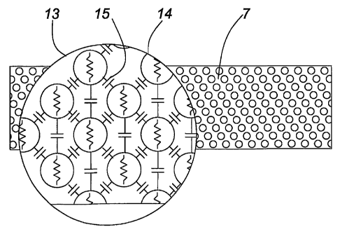
[0056] Figure 9 is a schematic depiction of a hypothetical, enlarged
cross-section of the substrate of an electrode according to the invention
depicting hypothetical capacitors and resistors that may make up such
sub strate.
DESCRIPTION OF THE PREFERRED EMBODIMENT
[0057] Figure 1 depicts a pictorial schematic layout for the electrical
circuit of the invention, when analyzed in terms of DC currents, before
taking into consideration polarization noise effects.
CA 02480257 2004-09-23
WO 03/079897 PCT/CA03/00426
[0058] All pickup electrodes are used to convey signals originating
inside a body 12 to an external reading device such as an ECG machine or
heart rate counter through a closed circuit which provides a voltage divider
network. The electrical signal inside the body can be called the body-
source, as represented by a voltage Vb. Analyzing this circuit for its DC
characteristics, the body source, along with the voltage divider required for
the pickup of the bio-signal is illustrated in Figure 1 wherein:
- Rs and R's are the skin resistance;
- F is the location of the body-to-electrode interface;
- Rc is the contact resistance at the interface F;
- Re is the electrode bulk resistance, and
- Ra is the resistance across which the output signal Va is measured.
[OOS~A] The end of the voltage divider, opposite to the electrode, is
connected to the body through Rr at point K. Though showing as a resistor,
Rr in particular may also be provided as an impedance having a significant
capacitance component to reduce its impedance in the frequency band of
interest. This closes the circuit to provide the voltage divider network. An
operational amplifier, IC1A, serves as the sensing electronics.
[0059] The total resistance Rt of the circuit is approximately given by
the sum of the sensing resistor Ra, the bulk electrode resistance Re, the skin
resistances Rs, R's plus the contact resistance Rc arising at the electrode-to-
skin interface. The contact resistance at the return electrode location I~ is
assumed to be minimal because the return electrode preferably establishes a
very high conductivity connection to the body.
m
CA 02480257 2004-09-23
WO 03/079897 PCT/CA03/00426
[0060] In the case of passive electrodes connected to an ECG machine,
Ra represents the ECG machine input resistance. In the case of active,
ohmic pickup electrodes possessing an on-board, internal buffer amplifier
acting as an impedance converter, Ra represents the combined resistance of
the sensing circuit as bridged by the sensing resistor.
[0061 ] In order to protect the sensing circuitry from overload voltages,
Ra rnay be paralleled by two parallel, reversely oriented diodes such as
Schottky, low leakage diodes exemplified by Panasonic MA198CT. Diodes
D 1, D2 are shown in Figure 8. At the low signal levels provided by the
pick-up electrodes, such diodes exhibit high forward resistances, having a
resistance of on the order of 10 exp 12-13 ohms. The forward resistance of
Schottky diodes before breakdown occurs is at on the order of 10 exp 13
ohms. By choosing diodes with a forward breakdown voltage that is above
the level of the signal of interest, the "reset" function of the input
resistance
of the high impedance amplifier can be improved.
[0062] It is often recommended for bio-signal pickup including ECG
that skin preparation such as cleaning, shaving and abrasion be performed to
ensure that the skin resistance (Rs) attains the lowest possible value. The
present invention represents a departure from the prior art by providing an
electrode that does not require substantial skin preparation to produce high
quality signals. However, naturally forming sweat can improve performance
and this effect can be accelerated by providing moisture at the electrode-to-
body interfaces, F, K.
22
CA 02480257 2004-09-23
WO 03/079897 PCT/CA03/00426
[0063] In Figure 2 the noise generating aspect of polarization is
modelled as a capacitor Cn which may be envisioned as having been
charged by a battery with fixed l~C voltage, Vn, which capacitor Cn is
randomly switched into and out of series connection with Re. Polarization
noise arises when Cn randomly discharges into the voltage divider.
[0064] The value of Ra may be chosen by the requirement that the
measured output signal Va should be at least generally half that of the body
source voltage Vb or preferably larger. For example, if it is desired that Va
should be in magnitude 95% of Vb, then Ra should be about 20 times the
value of Re. It is permissible, however, for Ra to be less than Re, but at the
expense of a reduced output signal Va.
[0065] When Ra and Re together are much greater than Rs etc, the
electrode output signal Va is approximately governed by the signal
distribution relationship:
Va = Vb [Ra/(Re+Ra)]
where Vb is the body voltage and Va is the sensed voltage (across Ra).
[0066] For reasons analogous to those discussed above in connection
with impedances of typical reading devices, the resistor Ra should not be
much larger than that required to satisfy signal size requirements because
overly large values for Ra can introduce noise or compromise the desired
signal-stabilizing and referencing properties of the invention.
[0067] The return electrode Rr contact at point K is not shown in
Figure 2 as being a source of noise for simplification. The return electrode
23
CA 02480257 2004-09-23
WO 03/079897 PCT/CA03/00426
preferably makes a very high conductance contact with the body. By
utilizing dual pick-up electrodes to effect common mode noise rejection,
noise effects arising at the contact K can be ignored. The reference
electrode at point K can preferably take the form of a low resistance,
passive, dry (or wet) electrode of standard ohmic type so long as it is used
in
combination with a differential noise rejection circuit. Alternately, it can
simply be an electrode according to the invention, but with minimal
resistivity.
[0068] Figure 3 illustrates a cross-sectional view of a coin-shaped or
disc-shaped electrode of the invention. The electrode is encapsulated with
an insulating layer 1 which is electrically resistive and waterproof. Several
encapsulating materials including non-conductive epoxy, plastic and rubber
compounds have been found suitable for this purpose. The electrode
possesses an internal conductive cap acting as a shield 2, which is
"grounded" i.e. connected to the circuit reference potential which is
connected to the reference electrode. A cable 3 carries power to, and signals
from the on-board electronic circuit 4. The circuit 4 is fixed on a 2-layer
printed circuit board 5 with a bottom conducting layer 6 conveniently
serving as the low resistance ohmic contact to the electrode substrate layer
7.
That substrate layer 7 is about 6 cm~2 in area.
[0069] A preferred material for substrate layer 7 is a moulded-rubber
sheet containing a suspension of fine carbon to render it mildly conducting
according to the invention. Various mixtures with desirable resistivities can
be made in accordance with the teachings of "Conductive Rubber and
Plastics", R.N. Norma, Elsevier Publishing Co. Amsterdam 1970.
24
CA 02480257 2004-09-23
WO 03/079897 PCT/CA03/00426
Successful electrodes have been constructed using olefin elastomers
including EPDM (Ethylene Propylene Diene Monomer), neoprene and
butyl-, nitrile, and silicone-based rubbers that are rendered slightly
conductive with carbon black, or with other conductive additives that form a
conductive matrix in the background, non-conductive, support material. The
invention however relates to any substrate materials possessing low bulk
conductivity of the desired value as well as the other appropriate
characteristics.
[0070] The substrate layer 7 may be bonded to the conducting layer 6
by way of a conductive adhesive. Alternately, substrate layer 7 can be
painted or moulded onto the circuit board conducting layer 6. The substrate
layer 7 may have a volume resistivity in the X-Y plane of the electrode
surface in the range 10 exp 3 ohm-cm to 10 exp 11 ohm-cm, which is a
primary range for the invention. The resistivity characteristics of the
invention are stipulated as being measured in the plane of the electrode
surface because polarization arises on this surface. The Re value of this
electrode of Figure 3 was approximately 1 Mohms impedance and was
employed with an Ra of approximately 1 Gohm.
[0071] The insulating layer 1 may extend to a point along the outer
edges of the electrode so as to present an insulating ring around the
substrate
on the body-facing side of the electrode. A grounding ring (not shown),
connected to the circuit ground, may surround the insulating ring, positioned
to contact the body and provide a supplementary or alternate primary
ground.
CA 02480257 2004-09-23
WO 03/079897 PCT/CA03/00426
[0072] Electrodes of the invention have the advantage of producing
very low 1/2-cell or polarization noise. This is believed to be due to the
poor conductivity of the substrate on the following basis. This basis is
presented as a theory that need not necessarily be correct.
[0073] An electrode based upon a conductive additive distributed
within an insulative background material can be envisioned as a parallel
array of many microscopic electrodes seen as series elements extending
from the body-facing side of the substrate to the sensor input. Each element
can be considered to terminate on a small capacitor C*n, representing the
1/2-cell capacitance due to the contact between the small element and the
body. Each electrode element also comprises a resistor R*e representing the
resistance of the overlying substrate layer responsible for conducting the
bio-signal into the sensor. The complete electrode is an inter- or cross-
connected parallel network of such elements with combined capacitance Cn
equal to the sum of all the C*n and combined resistance Re arising from the
interconnected sum of all the R*e.
[0074] An electrode of the invention with high resistivity (low
conductivity) can be considered to be a microscopic network of a few
interconnected, parallel electrode circuits suspended in a non-conducting
background material. At the electrode surface, the conductive links
terminate at small islands, surrounded by the background material. The
elemental capacitors Can that are responsible for polarization noise are
located at these small islands. Since the total polarization capacitance
generated by the electrode is the sum of the elemental capacitances, a
26
CA 02480257 2004-09-23
WO 03/079897 PCT/CA03/00426
substrate with high resistivity (low conductivity) produces a lesser total Cn
than an electrode of substrate with low resistivity.
[0075] Using the electrical schematic of Figure 2, Figure 4 sets forth a
graph which is intended to demonstrate the principle of the invention. While
based upon certain hypothetical assumptions, Figure 4 indicates how the
time constant for polarization noise, Tau, can be reduced by employing
increasingly larger volume resistivity values, Rho, for the body-facing
surface 10 of the pickup electrode.
[0076] Thus Figure 4 is a graph of a hypothetical time constant
ordinate, Tau, wherein Tau most accurately equals CnRt. However, for
simplification this graph has been prepared using the formula Tau = Cn (Re
+ Ra). This approximation becomes accurate when Rt essentially equals
Re+Ra.
[0077] This time constant Tau assumes an electrode substrate in the
form of a 10 cm square plate area and a 1 mm. The abscissa plots volume
resistivity, Rho, for the layer of the electrode occupying the gap between the
electrical circuit side conductive plate 6 of the electrode and the body side
of
the electrode. Both Tau and Rho are plotted on logarithmic scales.
[007] Re is assumed to be proportional to the bulk resistivity Rho (Re
equals Rho X thickness/area). Cn is assumed to be proportional to 1/Rho
exp 2/3. This is based on the assumption that surface area varies as a two-
thirds power of volume. The capacitance Cn is presumed to be proportional
27
CA 02480257 2004-09-23
WO 03/079897 PCT/CA03/00426
to the portion of the surface area occupied by islands of conductivity
connected to conductive pathways through the electrode.
[0079] In the case of conductive particles randomly suspended in a
volume of insulating medium, it is known that the surface density of
conductive particles is proportional to the volume particle density raised to
the power 2/3. The conductivity of such a medium is a highly non-linear
function of the particle concentration. In this case, the conductivity (1/Rho)
as a function of particle concentration undergoes a sharp increase at a
specific conductive additive concentration called the percolation threshold
(Pc). At lower concentrations, very few of the conductive particles
participate in conductivity through the layer because many occur in
isolation, with no significant electrical contact to neighbouring particles.
[0080] In the model: Cn varies as Rho exp -2/3, we have assumed that
the number of networked conductive particles is proportional to the DC
volume conductivity (1/Rho) and that the effective, conductive area of the
electrode is proportional to the number of networked conductive particles
that occur on the surface i.e. proportional to the number of networked
particles raised to the power 2/3. This results in Cn proportional to (1/Rho
exp 2/3).
[0081] On this basis, Figure 4 is plotted for demonstration purposes on
the initial premise that Cn has a value of 1 microfarad for a Rho value of 100
ohm-cm. Various curves for Tau are shown corresponding to fixed values
for Ra, e.g. 2, 20, 200 Mohms and 1 Gohm. Ra should generally exceed Re
and preferably be as high as 20 times Re, e.g. a signal distribution ratio
28
CA 02480257 2004-09-23
WO 03/079897 PCT/CA03/00426
between Ra and Re of approximately 95 percent. But achieving such a high
capture ratio is not essential.
[0082] Different values for Ra are relevant as the formula Tau = Cn x
Rt only reduces to Tau = Cn (Re + Ra) when Re and Ra dominate all other
resistances in the circuit. The other resistances include body resistance Rb,
contact resistance Rc (which is highly variable and may typically range on
the order of 50 kohms to 5 Mohms per cm2), and return electrode resistance
Rr. The total of such resistances will typically not exceed 3 Mohms, or
more certainly, 5 Mohms, for a large maj ority of persons. For
simplification, Rt is assumed to be equal to (Re+Ra) in plotting Figure 4.
For high values of Ra and Re, the signal distribution ratio Ra/(Re+Ra) is
essentially the signal capture ratio.
[0083] While unprepared skin resistance is typically estimated at 300
kohms per cm2, it can range below 100 kohms/cm2, and up to about 2
Mohms/ cm2. Accordingly, the curve for Ra = 2 Mohms does not meet the
assumption that Rt is essentially equal to(Re+Ra). However, for Ra = 20
Mohms, this equivalence is more nearly true. And even more so for Ra =
100 Mohms and higher.
[0084] Nevertheless, some degree of useful performance of the
invention can still be obtained in some cases where Ra values are as low as 2
Mohms, subject to the difficulty that common mode noise rejection may not
be as effective for such low values of Ra. On the other hand, it is preferable
that the value for Ra not exceed a 10 Gohm value, more preferably not
29
CA 02480257 2004-09-23
WO 03/079897 PCT/CA03/00426
exceed 5 Gohms, and even more preferably, be less than one Gohm. This is
to avoid the introduction of noise artifacts arising from static charges.
[0085] The curves all descend while the value for Cn falls as Rho
increases. Cn dominates the term Ra + Re while Re is less than Ra. But
when Re becomes larger than Ra, the curve for Tau changes towards
increasing values of Tau with increasing values of Rho. This curve for Tau
thereafter increases in Figure 4 at a rate proportional to Rho exp 1/3. The
"knee" in the curve identifies the shift from Ra being predominant over Re
to the stage where Re predominates over Ra.
[0086] Shown on both Figures 3 and 4 is a trace Tl in the form of a
line indicating the boundary where Ra = 20 Re. To the left of this trace, Ra
is greater than 20 Re. To the.right this distribution ratio drops below 20 to
1.
A second line T2 traces values for Ra = Re. For preferred high capture
ratios, electrodes of the invention should be designed to operate to the left
of
these traces.
[0087] As it is desirable to avoid variable performance arising from
variations in the skin Rs and contact Rc resistances, it is also preferable to
operate with Ra values above on the order of 2 Mohms, more preferably
above 20 Mohms and even more preferably above 200 Mohms.
[0088] As the object is to reduce the effect of polarization noise arising
from Cn, electrodes according to the invention should preferably have a Tau
of less than one second. More preferably the Tau should be less than 100
milliseconds and even more preferably 10 milliseconds or less.
CA 02480257 2004-09-23
WO 03/079897 PCT/CA03/00426
[0089] To complete the definition of the preferred operating regime of
the invention, it is believed that values for Rho in excess of 10 exponent 11
ohm-cm should be avoided due to the increasing noise effects arising from
slow discharge of static/tribo-electric charges, such as may develop across
dry skin.
[0090] The upper limit of the regime of substrate resistivity of the
invention, i.e. 10 expll, more preferably 10 exp 10 ohm-cm is believed to
define the practical limit for the realization of the advantages of the
invention. This is because the advantages of the high resistivity substrate,
namely the reduction of polarization effects, are countered by the onset of a
secondary noise generation mechanism i.e. triboelectricity, also called static
electricity, that is formed by contact between the virtually insulating
electrode substrate and the body. As the substrate resistivity Rho increases
above the order of magnitude 10 exp 10 ohm-cm and the corresponding Ra
increases, the reduction in the polarization effect increasingly becomes
counter-balanced by the increasing significance of triboelectric charges and
surface charge effects which create noise voltages.
[0091] Concurrent increases in Ra creates a situation whereby the
discharge times for these noise sources also increases. In fact, electrodes
with substrate resistivity substantially above the order 10 exp 10 ohm-cm
begin to operate akin to a capacitive mode. Thus it can be said that
electrodes of the invention, particularly for the purpose of ECG
measurements, operate in a "crossover" regime between ohmic and
capacitive operation.
31
CA 02480257 2004-09-23
WO 03/079897 PCT/CA03/00426
[0092] It has been found that experiments with electrodes of low-
capacitance type as specified in PCT application PCT/CA00/00981 (adopted
herein by reference) that fully capacitive operation is realized with
substrate
resistivities greater than 10 exp 14 ohm-cm and input bridging Ra values of
the order 10 exp 12 ohms. In these ranges in PCT application
PCT/CA00/00981 Ra is preferably limited to provide for the discharge of the
electrode capacitance when disturbed by noise signals occurring below the
frequency band of interest e.g. below 0.05 Hz.
[0093] It will be seen from Figure 4 that a preferred region for the
operation of an electrode according to the invention is in the lower portion
of
the defined area of the graph wherein:
1 ) Tau is minimal;
2) the distribution (and capture) ratio is higher;
3) Ra is sufficiently large so as to desensitize the electrode from
variations in skin and contact resistances, but not so large as to make the
system sensitive to static charge and tribo-electric effects or environmental
interference; and
4) Re is sufficiently large so as to achieve the above trade-offs,
namely: provide a reduced value for Tau, (thereby desensitizing the
electrode to noise arising from polarization effects) but not so large as to
extend the time period for the discharge of noise from static charge and
tribo-electric effects or reduce the capture ratio below 1 to 1.
32
CA 02480257 2004-09-23
WO 03/079897 PCT/CA03/00426
[0094] Figure 5 shows a variation over Figure 4 wherein a background
fixed capacitance of 30 picofarads is assumed to be present in addition to
Cn. This assumption allows for the presence of residual, intrinsic
capacitance at the electrode-to-body interface that arises from overall
geometry considerations and may hold static charge.
[0095] In Figure 5, to the right of the "knee", the curves for Tau
increase more rapidly than in Figure 4. Transverse traces for distribution
ratios of 20 to 1 (T 1 ), and 1-to-1 (T2) are shown on both Figures 4 and 5,
indicating that the preferred region for operation of electrodes of the
invention is not significantly modified by the assumption that Cn reaches a
minimum, constant value of 30 picofarads.
[0096] In terms of the preferred operating region of the invention, as
previously defined, it will be noted that Dunseath Jr., in IJ.S. patent
4,669,479, recommended use of an electrode material with a Rho not
exceeding 2 X 10 exp 5 ohm-cm and an Ra of greater than 10 Gohms. In
terms of the relevant surface layer of the electrode, the inventors do not
claim electrodes by themselves having a Rho of less than 2 X 10 exp 5
ohm-cm. However, in combination with the range of preferred values for
Ra, the invention may operate with Rho values of less than 2 X 10 exp 5
ohm-cm. It is believed that the invention will work with Rho values
commencing from about 10 exp 3 ohm-cm and higher in conjunction with an
electric circuit having the preferred values for the various components as
outlined above.
33
CA 02480257 2004-09-23
WO 03/079897 PCT/CA03/00426
[0097] While the invention has been described in terms of the DC
characteristics of the electrode and sensing resistor Ra, many of the elements
of the circuit may qualify as impedances wherein the reactive component of
the impedances arises from capacitive effects. A principal circuit
component in this regard is Re. Re in one simplified interpretation may be
considered to be bridged by a single parallel bulk capacitance Ce. In a more
elaborate analysis the electrode substrate may be modeled as depicted in
Figure 9. The actual capacitive character of the high resistivity substrate of
the invention has been tested and found to be highly complex. Capacitive
value measurements have been found to be frequency dependant.
[0098] Figure 9 addresses a possible explanation for the source of the
complexity of the impedance characteristics of an electrode made in
accordance with the invention. In the simplest view of a carbon-loaded
rubber 13, the particles 14 each have resistance, and the space between the
carbon particles 14 has a certain capacitance 15. This is depicted in Figure
9. In addition there will be some chains of particles which have purely DC
resistance (not shown).
[0099] The capacitors 15 are significant in value because capacitance
is inversely proportional to the insulating gap size. Since these particles
l4are very close together, their capacitance is large. The capacitors 15 are
in
a mass of series and parallel configurations, but when taken in totality
provide a specific, and possibly frequency dependent, bulk-capacitive
component for Ce.
34
CA 02480257 2004-09-23
WO 03/079897 PCT/CA03/00426
[0100] Such complexity does not, however, affect the time constant
Tau, arising from Cn. Rather, it may affect the capture ratio. In fact,
significant values for Ce will increase the capture ratio for higher frequency
signals.
[0101] In these circumstances it is believed that the DC analysis of the
circuits as provided fairly characterizes the presence of the invention.
[0102] Figure 6 shows simultaneous signals comparing standard gel
electrodes with two active electrodes according to the invention. The
different sets of electrodes were applied to skin of a patient at adjacent
locations on the chest just beneath each breast. The gel electrode sites were
prepared according to standard protocols for ECG procedures (top trace).
Such electrodes were applied to cleaned, abraded skin of the patient and
subsequently connected to one of the identical event recorders. The upper
trace shows the signal derived from the two passive medical adhesive gel
electrodes.
[0103] The lower trace shows the signal obtained by connecting the
second of the identical event recorders to two active electrodes of the type
illustrated in Figure 2. The electrodes of the invention were moistened with
a damp sponge and applied to adj acent unprepared skin of the same patient.
[0104] Each trace was recorded using the same type of single-channel
output commercially available event recorder connected through two-lead
wire cables to a pair of electrodes. The output signal in both cases was
CA 02480257 2004-09-23
WO 03/079897 PCT/CA03/00426
based on common mode noise rejection. During the time of the recording in
each case, the patient was in a state of motion.
[0105] The signal quality is significantly higher in the case of the
electrodes of the invention in that less noise is present.
[0106] Figure 7 depicts the band pass characteristics for an electrode
module built based on the design of Figures 2 and 8. Figure 7 shows that
signals applied to the electrode are delivered by the sensing circuitry with a
virtually flat band pass response over the range from 0.01 Hertz to over 20
kilohertz.
[0107] Figure 8 shows a differential input electronic circuit that
reduces or eliminates common mode noise. In Figure 8 two pick-ups similar
to that of Figure 2 are used to drive a differential amplifier pair IC1A,
IC2A.
The additional operational amplifier IC3A further conditions the signal for
transmission by shielded wire 3 to a display or recording device.
[0108] By use of this differential signal detection circuit, common
mode noise arising from the return electrode connection will be minimized.
CONCLUSION
[0109] The foregoing has constituted a description of specific
embodiments showing how the invention may be applied and put into use.
These embodiments are only exemplary. The invention in its broadest, and
36
CA 02480257 2004-09-23
WO 03/079897 PCT/CA03/00426
more specific aspects, is further described and defined in the claims which
now follow.
[0110] These claims, and the language used therein, are to be
understood in terms of the variants of the invention which have been
described. They are not to be restricted to such variants, but are to be read
as covering the full scope of the invention as is implicit within the
invention and the disclosure that has been provided herein.
37