Note: Descriptions are shown in the official language in which they were submitted.
CA 02480338 2004-09-23
WO 03/089564 PCT/GB03/01705
SUBSTRATE AND METHOD FOR MEASURING THE ELECTRO-
PHYSIOLOGICAL PROPERTIES OF CELL MEMBRANES
Technical field
The present invention provides a substrate and a method for
determining and/or monitoring electrophysiological properties of ion
channels in ion channel-containing structures, typically lipid membrane-
containing structures such as cells, by establishing an electrophysiological
measuring configuration in which a cell membrane forms a high resistive
seal around a measuring electrode, making it possible to determine and
monitor a current flow through the cell membrane. More particularly, the
invention relates to a substrate and a method for analysing the
electrophysiological properties of a cell membrane comprising a
glycocalyx. The substrate is typically part of an apparatus for studying
electrical events in cell meinbranes, such as an apparatus for carrying out
patch clanlp techniques utilised to study ion transfer channels in biological
membranes.
Background to the invention
Introduction
The general idea of electrically insulating a patch of membrane and
studying the ion channels in that patch under voltage-clamp conditions is
outlined in Neher, Sakmann, and Steinback (1978) "The Extracellular Patch
Clamp, A Method For Resolving Currents Through Individual Open
Channels In Biological Membranes", Pfluger Arch. 375;219-278. It was
found that, by pressing a pipette containing acetylcholine (ACh) against the
CONFIRMATION COPY
CA 02480338 2004-09-23
WO 03/089564 PCT/GB03/01705
2
surface of a muscle cell membrane, one could see discrete jumps in
electrical current that were attributable to the opening and closing of ACh-
activated ion channels. However, the researchers were limited in their work
by the fact that the resistance of the seal between the glass of the pipette
and
the membrane (10-50 MSZ) was very small relative to the resistance of the
channel (10 GSZ). The electrical noise resulting from such a seal is inversely
related to the resistance and, consequently, was large enough to obscure the
currents flowing through ion channels, the conductance of which are
smaller than that of the ACh channel. It also prohibited the clamping of the
lo voltage in the pipette to values different from that of the bath due to the
resulting large currents through the seal.
It was then discovered that by fire polishing the glass pipettes and by
applying suction to the interior of the pipette a seal of very high resistance
(1 to 100 GS2) could be obtained with the surface of the cell, thereby
reducing the noise by an order of magnitude to levels at which most
channels of biological interest can be studied and greatly extended the
voltage range over which these studies could be made. This improved seal
has been termed a`gigaseal', and the pipette has been termed a`patch
pipette'. A more detailed description of the gigaseal may be found in O.P.
2o Hamill, A. Marty, E. Neher, B. Sakmann & F.J. Sigworth (1981) "Improved
patch-clamp techniques for high resolution current recordings from cells
and cell-free membrane patches." Pflugers Arch. 391, 85-100. For their
work in developing the patch clamp technique, Neher and Sakmann were
awarded the 1991 Nobel Prize in Physiology and Medicine.
Ion channels are transmembrane proteins which catalyse transport of
inorganic ions across cell membranes. The ion channels participate in
processes as diverse as generating and timing action potentials, synaptic
transmission, secretion of hormones, contraction of muscles, etc. Many
pharmacological agents exert their specific effects via modulation of ion
channels. Examples include antiepileptic compounds such as phenytoin and
CA 02480338 2004-09-23
WO 03/089564 PCT/GB03/01705
3
laniotrigine, which block voltage- dependent Na+-channels in the brain,
antihypertensive drugs such as nifedipine and diltiazem, which block
voltage dependent Ca2+-channels in smooth muscle cells, and stimulators
of insulin release such as glibenclamide and tolbutamide, which block an
ATP-regulated K+-channel in the pancreas. In addition to chemically-
induced modulation of ion-channel activity, the patch clamp technique has
enabled scientists to perform manipulations with voltage-dependent
channels. These techniques include adjusting the polarity of the electrode in
the patch pipette and altering the saline composition to moderate the free
1o ion levels in the bath solution.
The patch clanzp technique
The patch clamp technique represents a major development in
biology and medicine, since it enables measurement of ion flow through
1s single ion channel proteins, and also enables the study of a single ion
channel activity in response to drug exposure. Briefly, in standard patch
clamping, a thin (approx. 0.5-2 m in diameter) glass pipette is used. The
tip of this patch pipette is pressed against the surface of the cell membrane.
The pipette tip seals tightly to the cell membrane and isolates a small
20 population of ion channel proteins in the tiny patch of membrane limited by
the pipette orifice. The activity of these channels can be measured
individually ('single channel recording') or, alternatively, the patch can be
ruptured, allowing measurements of the channel activity of the entire cell
membrane ('whole-cell configuration'). High-conductance access to the cell
25 interior for performing whole-cell measurements can be obtained by
rupturing the membrane by applying negative pressure in the pipette.
The Gigaseal
As discussed above, an important requirement for patch clamp
30 measurements of single-channel currents is the establishment of a high-
CA 02480338 2004-09-23
WO 03/089564 PCT/GB03/01705
4
resistance seal between the cell membrane and the glass micropipette
tip, in order to restrict ions from moving in the space between the two
surfaces. Typically, resistances in excess of 1 Gn are required, hence the
physical contact zone is referred to as a`gigaseal' .
Fonnation of a gigaseal requires that the cell membrane and the
pipette glass are brought into close proximity to each other. Thus, while the
distance between adjacent cells in tissues or between cultured cells and their
substrates generally is in the order of 20-40 nm (Neher, 2001), the distance
between the cell menlbrane and the pipette glass in the gigaseal is predicted
1o to be in the Angstrom (i.e. 10-10 m) range. The physico-chemical nature of
the gigaseal is not known. However, gigaseals may be formed between cell
membranes and a wide variety of glass types including quartz,
aluminosilicate, and borosilicate (Rae and Levis, 1992), indicating that the
specific chemical composition of the glass is not crucial.
Cell membj-ane structure
Cell membranes are composed of a phospholipid bilayer with
intercalated glycoproteins, the latter serving a multitude of functions
including acting as receptors for various agents. These membrane-spanning
glycoproteins typically comprise peptide- and glyco-moieties which extend
out from the membrane into the extracellular space, forming a so-called
`glycocalyx' layer around the phospholipid bilayer which reaches a height
of 20 to 50 nm and creates an electrolyte-filled compartment adjacent to the
phospholipid bilayer (see Figure 1). Thus, the glycocalyx forms a
hydrophilic and negatively charged domain constituting the interspace
between the cell and its aqueous environment.
CA 02480338 2004-09-23
WO 03/089564 PCT/GB03/01705
Cytoskeleton and glycocalyx
Immediately underneath the cell membrane is located the
cytoskeleton, a meshwork of actin filaments, spectrin, anchyrin, and a
multitude of other large structural molecules. One important role of the
5 cytoskeleton is to anchor certain integral membrane proteins and
glycoproteins to fixed positions within the membrane. However, it is
believed that intercalated membrane glycoproteins are free, within certain
limits (lipid micro domains or `rafts'; for a review see Simons and Toomre,
2000), to move laterally in the phospholipid bilayer. Indeed, such an
1o arrangement has been described as being `like protein icebergs in an ocean
of lipids'.
Effect of glycocalyx on gigasear formation
In conventional patch clamp methods, the initial point of contact
1s between the glass pipette tip (which has a wall thickness of approximately
100 nm) and the cell involves the glycocalyx. An estimation of the electrical
resistance, represented by the 150mM electrolyte contained in the inter-
space defined between the glass surface and the lipid membrane, by the
height of the glycocalyx (e.g. 20 to 40nm) results in 20-60 M. This
20 estimation is in agreement with experimental observations on smooth
surface quartz coated chips of the TEOS (Triethyloxysilane) type, which
routinely yield resistances in the order of 40 MSZ (or only 4% of a G92). In
this estimation, it is assumed that the electrolyte is present between the
lipid
membrane and a glass surface approximately of cylindrical shape with
25 diameter about l m and length about 3-10 m. Subsequent gentle suction
(< 20 hPa) applied to the pipette further increases the resistance, ideally
leading to a gigaseal. Gigaseal formation may take place rapidly on a time
scale of 0.1 to 10 s, or it may be a prolonged process completed only after
several successive rounds of increased suction pressure. The time course of
CA 02480338 2004-09-23
WO 03/089564 PCT/GB03/01705
6
the gigaseal formation, reflects the exclusion of glycoproteins from the
area of physical (membrane/pipette) contact by lateral displacement in the
`liquid-crystal' phospholipid bilayer. In other words, the elements of the
glycocalyx, i.e. glycoproteins, are squeezed out of the area of contact due to
the negative hydrostatic pressure applied to the pipette which forces the
phospholipid bilayer (the hydrophilic polar heads of the phospholipids)
against the glass surface (hydrophilic silanol groups).
However, sometimes the process of resistance increase proceeds only
up to formation of a quasi gigaseal (0.5 to 1 Gn). Empirically, application
1o of a large (50-70 mV; Penner, 1995) negative electrical potential to the
pipette at this point may lead to the final resistance increase terminating
with the gigaseal. In terms of the glycocalyx, the latter observation may be
explained by negatively charged domains of glycoproteins being displaced
laterally driven by the applied negative pipette potential. The strength of
the
electrical field (E) acting on the glycoproteins, i.e. the electrical field
from
pipette lumen to the surrounding bath is considerable:
E_ x_ 70 m V_ 700.000 V/ nz
V 100 nm
2o assuming a pipette tip wall thickness (x) of 100 nm and an applied pipette
potential (V) of -70 mV.
Conventional pipettes versus planar substrates
Recent developments in patch clamp methodology have seen the
introduction of planar substrates (e.g. a silicon chip) in place of
conventional glass micropipettes (for example, see WO 01/25769 and
Mayer, 2000).
Attempts to fonn gigaseals between planar silicon-based chips and
living cells have proven problematic (for example, see Mayer, 2000).
CA 02480338 2004-09-23
WO 03/089564 PCT/GB03/01705
7
However, success has been achieved in obtaining gigaseals between
artificial phospholipid vesicles which contain no exterior glycocalyx. This
finding indicates a critical importance of the glycocalyx in the gigaseal
formation process.
Hence, there is a need for improved planar substrates suitable for use
in patch clamp studies of cell membrane electrophysiology which permit the
formation of a gigaseal with cell membranes comprising a glycocalyx.
Suminar.y of the Invention
The present invention provides a substrate and a method optimised
for determining and/or monitoring current flow through an ion channel-
containing structure, in particular a cell membrane having a glycocalyx,
under conditions that are realistic with respect to the influences to which
the
cells or cell membranes are subjected. Thus, data obtained using the
substrate and the method of the invention, such as variations in ion channel
activity as a result of influencing the cell membrane with, e.g. various test
compounds, can be relied upon as true manifestations of the influences
proper and not of artefacts introduced by the measuring system, and can be
used as a valid basis for studying electrophysiological phenomena related to
the conductivity or capacitance of cell membranes under given conditions.
It will be understood that when the term `cell' or `cell membrane' is
used in the present specification, it will normally, depending on the context,
be possible to use any other ion channel-containing structure, such as
another ion channel-containing lipid membrane or an ion channel-
containing artificial membrane.
As discussed above, an important requirement for patch clamp
measurements of single-channel currents is the establishment of a high-
resistance gigaseal between the cell membrane and the substrate. A key
factor in formation of a gigaseal is the proximity of the cell membrane to
CA 02480338 2004-09-23
~
the substrate, wh,ich is turn is dependent on the size of the area of contact
between the cell membrane and the substrate.
The physical area of contact between the cell membrane and a plaraaz
s silicoti chip (about l. m width of contact rim; see Figure 2, right hand
diagram) with a smoothly rounded, fiwel-Yike orifice is much larger than
that formed between a cell membrane and a glass xzzicropxpette (about 100
Fun width; Figure 2, left hand diagram.). This results in the force per unit
area being considerably xeduced in the chip zelative to the pipette
io configuration, ax-.d the number of intercalated glycoproteins in the
contact
area being much larger, effectively preventing the required .A,xxgstrom
distance between the phospholipid bilayer and the substrate surface
imperative for the formation of a gigaseal.
15 The present invention seeks to address this problem by providing a
planar substrate (e.g. a silicon-based chip), suitable for patch clamp stndies
of the electrophysiological properties of cell membrane, which is designed
to provide a reduced area of contact with the c,ell zuezn.bzaue, thereby
promoting tiae formation of a gigaseal.
Thus, a i=xzst aspect of the invention pxovides a substantially planar
substrate for use in patoh clamp analysis of the electrophysiologzcal
properties of a cell merribrane compzzsing a glycocalyx, wherein the
substrate comprises an aperture having a rim defini.ng the aperture, the rim
being adapted to form a gigaseal upon contact with the cell membrane, the
rim protruding from the plane of the substrate to a height in excess of tlae
thickness of the glycocalyx.
In a preferz'ed embodiment, the substrate is a szlicon-based chip.
AMENDED SHEET
CA 02480338 2004-09-23
9
In the present c4ntcxt, the term gigaseal nozmaDy jn.dicates a seal of
a least IC,r ohm, and this is the size of seal normally aimed at as a
miniar~~;nx.n,
but for certain types of measurements where the cnzre,nts are large, lower
values may be sufficient as threshold values.
s
By `glycocalyx' we mean the layer created by the peptide- and
glyco-moieties, which exten.d into the eh-tracellu3.ax space from the
glycoproteins in the lipid bilayer of the cell membxane.
Preferably, the .rixrx. extends at least 20mza., at least 30 nm, at least 40
nm, at least 50 nm, at least 60 nm, at least 70 nrn, at least 80 nm, at least
90
zama or at least 100 nm above the plane of the substxate,
,A,dvantageously, the rim is shaped stzch that the area of physical
contact between the substrate and the cell xnextabrane is minisiaised, thereby
favouwrzng penetration of the glycocalyx and formation of a gi.gasea,l.
It will be appreciated by persons skilled in the art that tb.e rim may be
of any suitable cross-sectional profile. For example, the walls of the rxm
2o may be tapexed or substantially pa.ral,lel . Likewise, the uppermost tip of
the
rixra, may take several shapes, for exaznple it may be dome-shaped, flat or
pointed. Furthermore, the rim protrusion may be substantially perpendicular
to, oblique, or parallel with the plane of the substrate. A parallel
protruding
rim may be Iocated at or near to the mouth of the aperture or, alternatively,
positioned deeper into the aperture. Convenien.tly, the width of the rim is
between 10 and 200 nm.
It will be further appreciated by persons skilled in the art that the
aperture should have dimensions which do zaot perniit ain intact cell to pass
so through the planar su.bstrate,
AMENDED SHEET
CA 02480338 2004-09-23
WO 03/089564 PCT/GB03/01705
Preferably, the length (i.e. depth) of the aperture is between 2 and 30
m, for example between 2 and 20 m, 2 and 10 gm, or 5 and 10 gm.
5 The optimal diameter of the aperture for optimal gigaseal formation
and whole cell establishment will be dependent on the specific cell type
being used. Advantageously, the diameter of the aperture is in the range 0.5
to 2 .m.
The substrate of the invention will typically be a component used in
1o an apparatus for carrying out measurements of the electrophysiological
properties of ion transfer channels in lipid membranes such as cells.
The apparatus may be designed to provide means for carrying out a
large number of individual experiments in a short period of time. This is
accomplished by providing a microsystem having a plurality of test
confinements (i.e. rimmed apertures for contacting cells) each of which
having sites comprising integrated measuring electrodes, and providing and
suitable test sample supply. Each test confinement may comprise means for
positioning cells, for establishment of gigaseal, for selection of sites at
which giga-seal has been established, measuring electrodes and one or more
reference electrodes. Thereby it is possible to perform independent
experiments in each test confinement, and to control the preparation and
measurements of all experiments from a central control unit such as a
computer. Due to the small size of the test confinements, the invention
permits carrying out measurements utilising only small amounts of
supporting liquid and test sample.
The substrate of the invention can be made of any material suitable
for a wafer processing technology, such as silicon, plastics, pure silica and
other glasses such as quartz and PyrexTM or silica doped witll one or more
dopants selected from the group of Be, Mg, Ca, B, Al, Ga, Ge, N, P, As.
Silicon is the preferred substrate material.
CA 02480338 2004-09-23
WO 03/089564 PCT/GB03/01705
11
In a preferred embodiment of the first aspect of the invention, the
surface of the substrate and/or the walls of the aperture are coated with a
material that is well suited for creating a seal with the cell membrane. Such
materials include silicon, plastics, pure silica and other glasses such as
quartz and PyrexTM or silica doped with one or more dopants selected from
the group of Be, Mg, Ca, B, Al, Ga, Ge, N, P, As and oxides from any of
these. Preferably, the substrate is coated, at least in part, with silicon
oxide.
In a further preferred embodiment of the first aspect of the invention,
lo the planar substrate has a first surface part and an opposite second
surface
part, the first surface part having at least one site adapted to hold an ion
channel-containing structure, each site comprising an aperture with a rim
and having a measuring electrode associated therewith, the substrate
carrying one or more reference electrodes, the measuring electrodes and the
reference electrodes being located in compartments filled with electrolytes
on each side of the aperture, the measuring electrodes and the respective
reference electrode or reference electrodes being electrodes capable of
generating, when in electrolytic contact with each other and when a
potential difference is applied between them, a current between them by
2o delivery of ions by one electrode and receipt of ions by the other
electrode,
each of the sites being adapted to provide a high electrical resistance seal
between an ion channel-containing structure held at the site and a surface
part of the site, the seal, when provided, separating a domain defined on one
_ side of the ion channel-containing structure and in electrolytic contact
with
the measuring electrode from a domain defined on the other side of the ion
channel-containing structure and in electrolytic contact with the respective
reference electrode so that a current flowing through ion channels of the ion
channel-containing structure between the electrodes can be determined
and/or monitored, the electrodes being located on each side of the substrate.
CA 02480338 2004-09-23
Examples of the general deszp of the preferred ezxzbodixn.ent of the
flrst aspect of the iriveation wherein the substrate comprises integral
electrodes (but withoiit the rimmed aperture feature of the present
s invention) are described in WO 01/25769.
A second aspect of the invention provides a method of amaldng a
substantially plazaar substrate for use in patcb, clarnp analysis of the
electzophysiological properties of a cell membrane comprising a
1o glycocalyx, wherein the substrate comprises an aperture having a rim
defining the aperture, the rim being adapted to form a gigaseal upon contact
with the cell membrane, the method comprising the steps of.
(i) providing a sabstrate template;
(ia) forming an aperture in the template; and
1s (iii) forming a rim around the aperture such that the rim protrudes
i'xom the substrate to a]aeight in excess of the thicl;,o.ess of the
glycocalyX.
Preferably, the substrate is ma.nufaetcrred usirig silicon micro
2o fabricatioia technology "Madou, M., 2001 ".
It wz.ll be appreciated by persons sldlled in the art that steps (ii) and
(iii) may be pexformed sequentially (i.e. in temporally separate steps) or at
the same time.
2s
Advantageously, step (ii) comprises forming an aperture by use of an
iuductively coupled plasma (ICP) deep reactive zo,u etch process. "Laermer
F. and Schilp, A., DE4241045"
Wlaen it is required to form a substantially vertical protrusion relative
so to the plane of the substrate, the method comprises an intermediate step of
a
AMENDED SHEET
CA 02480338 2004-09-23
13
directzon.al and selective etching of the front side of the substrate causing
a
removal of a ixaaskiag layer on the front side of the substrate, and further
proceediuo.g the prescribed protrttsxora distance into the underlying
substrate.
As a result of a faster etch rate of silicon compared to that of the s
masldzag material, the maskaxzg material will be left inside tb.e aperture,
and
prot,rude from the surface. An overall surface coating can subsequently be
appl'zed.
'When it is required to form a protrusion lying substantially in the
plane of the substrate, the x.n.ethod comprises an intezmediate step of using
lo Inductively Coupled Plasma (ICP) etch or Advauced Silicon Etch (ASB) for
the fozrzaation of the pore, wlaore the repetitive alternation of etching and
passivation steps characterising these metbods, wil.l result i.n, some
scalloping towards the mouth of the apemue. By suitable adjtxstment of the
process parameters, the scalloping oan result in an inward in plane
15 protrusion of the rim.
Again, an overall surface coating can subsequently be employed.
Conveniently, the method ffinther comprises coating the surface of the
substrate (e.g. with silicon oxide), either before or after forrnation of the
apcrture and/or rim. Alternatively, step (iii) is perforzn.ed at the same time
as
21) coating the substrate.
Such coatings may be deposited by use of plasma enhanced chemical
vapour deposztion (PECVD) andlor by use of low pressure chemical vapour
deposition (LPCVD).
25 The preferred embodiment of the first aspect of the i-aventzon wherein
the substrate coznprises integral electrodes may be mtznufactured as
described in WO 01/25769).
AMENDED SHEET
CA 02480338 2004-09-23
14
A tbizd aspect of the invention provides a method for analysing the
electrophysiological lazopex-ties of a cell na.embzazae comprising a
glycocalyx, the xa.ethod comprising the followizag steps:
(z) making a substantiaU.y planar substrate for use in patch clamp 5 analysis
of th.e electrophysiological properties of a cell membrane
comprising a glycocalyx, wherezza, the substrate comprises an aperture
having a rim defuaua.g the aperture, the rim beiw.g adapted to form a
gigaseal upon contact with the cell membrane, the method comprising
t.he steps of
to (ii) providing a substrate template;
(iii) forming an apertuxe in the template; and
(iv) fom-in.g a ria.n around the aperture sucla that the riua protrudes from
the substrate to a height in excess of the thiclmess of the glycocalyx,
(v) contacting the cell membra,ue with the rim of au apertuze of the
1s substrate such that a gigaseal is foxxned between the cell membrane
and the subsfirate; and
(vi) measuriag the electrophysiological properties of the cell
membrane.
20 In a preferred embodiment of the third aspect of the invention, there
is provided a method of establishing a wlaoae cell measuring configuration
for determining and/or monitoring an electrophysiological property of one
or more ion chamels of one or more ion channel-containing structures, said
met'hod comprising the steps of-
25 (i) providiug a substrate as deftned above;
(ii) supplying a cazxier liquid at orne or more apertures, said carrier
liquid containing one or more ion claaun.el-containing structures;
(ia.i,) positioning at least one of the ion channel-contaWi.zag structures at
a correspon.diazg number of aperkures;
AMENDED SHEET
CA 02480338 2004-09-23
14a
(iv) checking for a high eiectrical resistartce seal between an ion
channel-conta.iuazag structure iZald at a site (i.e. aperture) and tbe
surface part of the site (i.e. rim) v;+ith which the bigh electrical
resistance seal is to be provided by successively applying a first
electric potential difference between the measuring electrode
associated wi.th the site amd a reference electrode, monitoring a first
current flowing between said measuring electrode and said reference
electrode, and comparing said
AMENDED SHEET
CA 02480338 2004-09-23
WO 03/089564 PCT/GB03/01705
first current to a predetermined threshold current and, if the first
current is at most the predetermined threshold current, then approving
the site as having an acceptable seal between the ion cannel-containing
structure and the surface part of the site; and
5
(v) establishing a whole-cell configuration at approved site(s),
whereby a third current flowing through ion channels of the ion channel-
containing structure between the measuring electrode and the reference
1o electrodes can be detennined and/or monitored.
An ion channel-containing structure (e.g. a cell) in a solution may be
guided towards a site on a substrate either by active or passive means. When
the ion channel-containing structure makes contact with aperture rim, the
contact surfaces form a high electrical resistance seal (a gigaseal) at the
site,
15 such that an electrophysiological property of the ion channels can be
measured using electrodes. Such an electrophysiological property may be
current conducted through the part of membrane of the ion channel-
containing structure that is encircled by the gigaseal.
A whole-cell configuration may be obtained by applying, between
the measuring electrode associated with each approved site and a reference
electrode, a series of second electric potential difference pulses, monitoring
a second current flowing between the measuring electrode and the reference
electrode, and interrupting the series of second electric potential difference
pulses whenever said second current exceeds a predetennined threshold
value, thereby rupturing the part of the ion channel-containing structure
which is closest to the measuring electrode.
Alternatively, the whole-cell configuration may be obtained by
subjecting the part of the ion channel-containing structure which is closest
to the measuring electrode to interaction with a aperture forming substance.
CA 02480338 2004-09-23
WO 03/089564 PCT/GB03/01705
16
It should be noted that in the present context, the term
"whole-cell configuration" denotes not only configurations in which a
whole cell has been brought in contact with the substrate at a measuring site
and has been punctured or, by means of a aperture-forming substance, has
been opened to electrical contact with the cell interior, but also
configurations in which an excised cell membrane patch has been arranged
so that the outer face of the membrane faces "upwardly", towards a test
sample to be applied.
As the measuring electrode associated with a site may be one of a
lo plurality of electrodes on the substrate, and the ion channel-containing
structure may be one of many in a solution, it is possible to obtain many
such prepared measuring set-ups on a substrate. A typical measurement
comprises adding a specific test sample to the set-up, for which reason each
measuring set-up is separated from other measuring set-ups to avoid mixing
of test samples and electrical conduction in between set-ups.
In use, the addition of cell-supporting liquid and cells to the substrate
is carried out in one of the following ways. In a preferred embodiment, the
test confinements are accessible from above, and droplets of supporting
liquid and cells can be supplied at each test confinement by means of a
2o dispensing or pipetting system. Systems such as an ink jet printer head or
a
bubble jet printer head can be used. Another possibility is an nQUAD
aspirate dispenser or any other dispensing/pipetting device adapted to dose
small amounts of liquid. Alternatively, supporting liquid and cells are
applied on the substrate as a whole (e.g. by pouring supporting liquid
containing cells over the substrate or immersing the substrate in such),
thereby providing supporting liquid and cells to each test confinement.
Since the volumes of supporting liquid and later test samples are as small as
nanolitres, water vaporisation could represent a problem. Therefore,
depending of the specific volumes, handling of liquids on the substrate
should preferably be carried out in high humidity atmospheres.
CA 02480338 2004-09-23
WO 03/089564 PCT/GB03/01705
17
In another embodiment, the cells are cultivated directly
on the substrate, while immersed in growth medium. In the optimal case,
the cells will form a homogeneous monolayer (depending on the type of
cells to be grown) on the entire surface, except at regions where the surface
intentionally is made unsuitable for cell growth. The success of cultivation
of cells on the substrate depends strongly on the substrate material.
In still another embodiment, an artificial membrane with
incorporated ion channels may be used instead of a cell. Such artificial
membrane can be made from a saturated solution of lipids, by positioning a
1o small lump of lipid over an aperture. This technique is thoroughly
described
by Christopher Miller (1986) Ion Channel Reconstitution, Plenum 1986,
p. 577. If the aperture size is appropriate, and a polar liquid such as water
is
present on both sides of the aperture, a lipid bilayer can form over the
aperture. The next step is to incorporate a protein ion channel into the
bilayer. This can be achieved by supplying lipid vesicles with incorporated
ion channels on one side of the bilayer. The vesicles can be drawn to fusion
with the bilayer by e.g. osmotic gradients, whereby the ion channels are
incorporated into the bilayer.
Obtaining good contact between the cell and a glass pipette, and
thereby creating a gigaseal between a cell and the tip the pipette, is well
described in the prior art. In order to draw the cell to the tip of the
pipette,
as well as to make the necessary contact for obtaining the gigaseal, it is
normal to apply suction to the pipette. However, with the planar substrates
of the present invention mere contact between the cell membrane and the
substrate, typically ultra-pure silica, can be sufficient for the cell to make
some bonding to the surface and create a gigaseal.
The positioning of a cell over an aperture in the substrate can be
carried out by electrophoresis, where an electric field from an electrode
draws the charged cell towards it. Negatively charged cells will be drawn
towards positive electrodes and vice versa. The electrostatic pull can also
CA 02480338 2004-09-23
WO 03/089564 PCT/GB03/01705
18
act as guiding means for a group of electrodes. Alternatively, within a
test confinement, a hydrophobic material may cover the surface of the
substrate except at areas just around electrodes. Thereby, cells can only bind
themselves on electrode sites. It is possible to apply both of these methods
simultaneously or optionally in combination with a suitable geometrical
shape of the substrate surface around electrodes, to guide the sinking cells
towards the electrode.
Alternatively, the positioning of a cell over an aperture in the
substrate can be carried out by electro-osmosis.
If suction is applied, it draws the cell to the aperture and establishes a
connection between the cell and the aperture, creating a gigaseal separating
the aperture inside and the solution. The gigaseal may take any form, e.g.
circular, oval or rectangular. Where the substrate comprises integral
electrodes, the supporting liquid may make electrical contact between the
cell membrane and a reference electrode. The cell may be deformed by the
suction, and a case where the cell extends into (but does not pass through)
the aperture may be desired if controlled.
Using the substrates and methods of the invention, the activity of the
ion channels in the cell membrane can be measured electrically (single
channel recording) or, alternatively, the patch can be ruptured allowing
measurements of the channel activity of the entire cell membrane (whole
cell recording). High-conductance access to the cell interior for performing
whole cell measurements can be obtained in at least three different ways (all
methods are feasible, but various cells may work better with different
approaches):
(a) The membrane can be ruptured by suction from the aperture side.
Subatmospheric pressures are applied either as short pulses of
increasing strength or as ramps or steps of increasing strength.
Membrane rupture is detected by highly increased capacitative current
CA 02480338 2004-09-23
WO 03/089564 PCT/GB03/01705
19
spikes (reflecting the total cell membrane capacitance) in response
to a given voltage test pulse;
(b) Membrane rupture by applied voltage pulses. Voltage pulses are applied
either as short pulses of increasing strength (mV to V) and duration (gs
to ms), or as ramps or steps of increasing strength, between the
electrodes. The lipids forming the membrane of a typical cell will be
influenced by the large electrical field strength from the voltage pulses,
whereby the membrane to disintegrates in the vicinity of the electrode.
Membrane rupture is detected by highly increased capacitative current
spikes in response to a given voltage test pulse.
(c) Permeabilization of membrane. Application of aperture-forming
substances (for example antibiotics such as nystatin or amphotericin B),
by e.g. prior deposition of these at the site. Rather than by rupturing the
membrane, the membrane resistance is selectively lowered by
incorporation of permeabilizing molecules, resulting in effective cell
voltage control via the electrode pair. The incorporation is followed by
a gradually decreasing total resistance and an increasing capacitance.
Where the substrate comprises a plurality test confinements each
comprising an aperture, test samples may be added to each test confinement
individually, with different test samples for each test confinement. This can
be carried out using the methods for applying supporting liquid, with the
exception of the methods where supporting liquid are applied on the
substrate as a whole.
Upon positioning the cell in a measuring configuration, several
electrophysiological properties can be measured, such as current through
ion channels (voltage clamp), or capacitance of ion channels containing
membranes. In any case, a suitable electronic measuring circuit should be
CA 02480338 2004-09-23
provided. The person skilled in the art will be able to select such suitable
measuring circuit.
A fourth aspect of the inveution provides a kit for perform.ing a method
5 according to Claim 24, the lcit comprising a substantially planar substrate
for we ia patch clamp analysis of the electrophysiological properties of a
celJ membrane comprisaxag a glycocalyx, wherein the substrate comprises an
aperture havitig a rim defining the aperture, the rim being adapted to fo= a
gigaseal upon contact with the cell membrane, the rim protruding from the
zo plane of the substrate to a height in excess of the tbicl;ness of the
glycocalyx
and ome or more media or rea.gents for performing patch clamp studies.
Preferably the kit comprises a plurality of substxates.
ts The invention will now be descri.bed with reference to the followln;g
szon-limiting examples and figures:
Figure 1, sbows the cell wzth a patch pipette attaclaed. T-a the gigaseal
zone, (indicated by shaded axea at point of coratact between the pipette tip
and the cell meznbrane) the glycoproteins of the glycocalyx have beera
20 displaced laterally to aJ,low direct contact between the membrane
phospholipid bilayer and the pipette;
Figures 2a and 2b show a cell attached to either a pipette tip (Figure 2a)
or a planar substrate (Figure 2b). The area of contact betweeia the ce3j
mexo;bzane and substrate surface is considerably larger in the substrate
configuratioza (Figure 2b) than in the pipette configuration (Figure 2a).
Figure 3 shows the variation in actua,t pipette resistance for each
intended resistab.ce set;
Figure 4 shows Gigaseal success rate versus pipette resistance;
Figure 5 shows the success rate of whole-cell establishment (fro;m
3o successful gigaseals) ver.sus pipette resistaxa.ce;
AMENDED SHEET
CA 02480338 2004-09-23
20a
Figure 6 shows the tiaaae-dependence of gzgaseal formation with
different apemue sizes, the error bars ztadacafino the standard deviation from
the mean;
AMENDED SHEET
CA 02480338 2004-09-23
WO 03/089564 PCT/GB03/01705
21
Figure 7 shows an example of a cell attached to a planar
substrate with a protruding rim flanking the aperture. The gigaseal
formation zone is very confined;
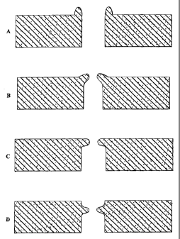
Figures 8a, 8b, 8c & 8d show four different aperture designs (die
transactions) including a protruding rim: vertical rim (Figure 8a); oblique
rim (Figure 8b); horizontal rim (Figure 8c); and embedded rim (Figure 8d).
Figure 9 shows a design without protrusion but with a rim sufficiently
sharp (r=25-100 nm) to reduce the membrane/substrate contact zone to 50-
200 nm. The aperture angle (0) is 45 to 90 degrees;
Figure 10a and Figure 10b are scanning electron micrographs of
substrate with long pores with a protruding rim in the plane of the surface
using ICP and LPCVD for surface modification; and
Figure 11 is a scanning electron micrograph of a substrate with long
pores with a protruding rim out of the plane of the surface using ICP and
LPCVD for surface modification.
2o EXAMPLES
The present invention identifies three factors that are important for
gigaseal formation and whole cell establishment in patch clamp
measurements performed on living cells containing glycocalyx in the cell
membrane:
1. The length of the aperture should be sufficiently long in order to
prevent the relatively elastic cells to be moved through the orifice upon
application of suction.
CA 02480338 2004-09-23
WO 03/089564 PCT/GB03/01705
22
2. There also appears to exist an optimal aperture size for gigaseal
formation and whole cell establishment which relates to the elastic
properties of the cell membrane and the cell type being studied.
3. The aperture of the planar substrate should be defined by a rim
capable of displacing the glycocalyx when approaching the cell surface.
Each factor is discussed below:
Length of the aperture
The length (i.e. depth) of the aperture, defined by the membrane
thickness of the chip, is also important. Low aspect ratio designs (short
apertures) suffer from the disadvantage that cells, upon positioning and
subsequent suction, have a tendency to move through the hole due to their
inherent elasticity. Studies have demonstrated that this problem may be
effectively obviated by using longer apertures, typically in excess of 2 gm
(data not shown).
Deterfnination of optimal aperture size
To determine the optimal aperture size for obtaining gigaseal and
whole cell configurations we have compared the success rates for achieving
them in a standard patch-clamp set-up, using patch pipettes of varying size.
The experiments were performed on HEK293 cells adhered to coverslips,
immersed in sodium Ringer solution. Borosilicate capillaries (Hilgenberg,
Cat No. 1403573, L= 75mm, OD = 1.5mm, ID = 0.87mm, 0.2mm filament)
were used to make pipettes. Pipette resistance was used as an indicator of
relative aperture size; pipettes with intended resistances of 0.5, 1, 2, 5, 10
and 15 MSZ were fabricated. At the time of measurement, the actual pipette
CA 02480338 2004-09-23
WO 03/089564 PCT/GB03/01705
23
resistance was noted and the average actual pipette resistance for each set,
along with the standard deviation from the mean, is shown in Figure 3.
Figure 4 shows the dependence of gigaseal and whole-cell success
rates on the pipette aperture resistance aperture size). The number of
experiments performed for each data set is shown above the data points.
The results show that pipettes with a resistance of 5 MSZ were optimal for
both gigaseal formation and whole cell establishment, while resistances
above 5, and up to 15 MS22, resulted in an approximately 20% drop in the
success rate. Reduction of pipette resistance below 5 MS2, was more
lo deleterious; A resistance of 2 MS2 gave a success rate or 50%, 37% lower
than for 5 M92, while resistances of 1 M12 or below resulted in virtually no
gigaseal formation at all.
Figure 5 shows the percentage of whole-cells formed from
experiments in which gigaseals were successfully formed (i.e. discounting
those that did not reach gigaseal). Data indicate that although 5 MS2
pipettes had the highest whole-cell success rate, the other aperture sizes had
only slightly lower successes.
The effect of pipette resistance on the time taken to reach a G92
resistance was also examined (see Figure 6). The results show that the 2
MO pipettes took significantly longer to reach gigaseal than did pipettes of
5, 10 or 15 M. The similarity of the results for the 5, 10 and 15 MSZ
pipettes indicates that increasing the aperture size within this range does
not
affect the time take to reach gigaseal.
The results clearly show that the success of gigaseal formation is
dependent on the size of the pipette aperture. The 5 M92 pipettes had the
optimal aperture size, and sizes greater than this (i.e. with lower
resistances)
resulted in a marked reduction is successful gigaseal formation.
Although the above experiments were performed using conventional
glass micropipettes, the results can be extrapolated to planar substrates for
use in patch clamp experiments. Thus, the results indicate that apertures in
CA 02480338 2004-09-23
WO 03/089564 PCT/GB03/01705
24
the chip system should, in general not measure larger than the apertures
of the 5 MQ pipettes. However, pipettes smaller than the 5 MS2 ones still
performed fairly well, although they were significantly worse. Therefore,
making the chip aperture slightly smaller than the 5 Mo pipettes would be
less deleterious than making it larger.
Varying the pipette aperture size appeared to have less effect on
whole-cell formation. Although the success of whole-cell formation was
highest in 5 MSZ pipettes, for pipettes from 2 MQ to 15 MSZ, there was only
a slight reduction in success rate.
It was also observed that the pipette aperture size had an effect on the
time taken to reach a GS2 resistance. Pipettes of 5 and 15 MS2 took similar
times to reach gigaseal, but those of 2 MQ took 2.5 to 3 times longer.
Microscopy of the glass pipettes used in the experiments revealed
that pipettes exhibiting 5 MS2 resistance had an aperture size of the order of
0.5-1 m. It is, however, expected that the optimal aperture size is related
to
the cell type and cell size.
The success-rate for obtaining gigaseals in conventional patch clamp
experiments is typically high, often around 90%, when patching cultured
cells like HEK or CHO. Based on the above considerations, it is expected
that comparable success-rate on planar chips may be achieved using an
aperture geometry mimicking that of a conventional pipette tip orifice. Such
a geometry would comprise a protruding rim flanking a 0.5 to 1 m
aperture hole. Moreover, the length (i.e. depth) of the aperture should
preferably be in excess of 2 gm.
Production of planarpatch-clamp substrates
A preferred method of producing the planer patch-clamp substrates
of the invention is by using silicon (Si) wafer micro-fabrication and
processing methods, which allow Si surfaces to be coated with silicon oxide
CA 02480338 2004-09-23
WO 03/089564 PCT/GB03/01705
effectively forming a high quality glass surface. Preferably, long pores
and the surface modification can be made by using ICP (Inductively
Coupled Plasma) and LPCVD (Low Pressure Chemical Vapour
Deposition). Long apertures with a protruding rim can be made by using
5 ICP to make the poreand RIE (Reactive Ion Etch) to form the protruding
rim, combined withLPCVD to make the surface modification.
(a) Example process recipe for long apertures with a protruding rim in
the plane of the surface using ICP and LPCVD for surface
10 modification (Fig.lOa and Fig.10b).
1. Starting substrate: single crystal silicon wafer, crystal orientation
<100>.
2. One surface of the silicon is coated with photoresist and the
15 pattern containing the aperture locations and diameters is
transferred to the photoresist through exposure to W light.
3. The aperture pattern is transferred to the silicon with Deep
Reactive Ion Etch (DRIE) or Advanced Silicon Etching (ASE)
using an Inductively Coupled Plasma (ICP), resulting in deep
20 vertical pores with a depth of 1-50 m.
4. The silicon surface is coated with a etch mask that will with stand
KOH or TMAH solution. As an example this could be silicon
oxide or silicon nitride.
5. The opposite side_of the wafer (the bottom side) is coated with
25 photoresist and a pattern containing the membrane defining
openings in the silicon nitride is transferred to the photoresist
through exposure to UV light.
6. The wafer is etched away on the bottom side of the wafer in the
regions defined by the openings in the photoresist, using a
CA 02480338 2004-09-23
WO 03/089564 PCT/GB03/01705
26
suitable pattern transfer process. As an example this could be
Reactive Ion Etch (RIE).
7. The wafer is etched anisotropically in a KOH or TMAH solution,
resulting in a pyramidal opening on the bottom side of the wafer.
The timing of the etching defines the thickness of the remaining
membrane of silicon at the topside of the wafer. Alternatively
boron doping can be used to define an etch stop, giving a better
control of the thickness.
8. The etch mask is remove selectively to the silicon substrate.
9. The silicon is coated with silicon oxide, either through thermal
oxidation, with plasma enllanced chemical vapor deposition
(PECVD) or with LPCVD.
Alternatively the substrate can be fabricated through the following process:
1. Starting substrate: single crystal silicon wafer.
2. One surface of the silicon is coated with photoresist and the
pattern containing the aperture locations and diameters is
transferred to the photoresist through exposure to UV light.
3. The aperture pattern is transferred to the silicon with Deep
Reactive Ion Etch (DRIE) or Advanced Silicon Etching (ASE)
using an Inductively Coupled Plasma (ICP), resulting in deep
vertical pores with a depth of 1-50 m.
_ 4. The opposite side of the wafer (the bottom side) is coated with
photoresist and a pattern containing the membrane definitions is
transferred to the photoresist through exposure to UV light.
5. The wafer is etched anisotropically using Deep Reactive Ion Etch
(DRIE) or Advanced Silicon Etching (ASE) using an Inductively
Coupled Plasma (ICP), resulting in a cylindrical opening on the
bottom side of the wafer. The timing of the etching defines the
CA 02480338 2004-09-23
WO 03/089564 PCT/GB03/01705
27
thickness of the remaining membrane of silicon at the topside
of the wafer.
6. The silicon is coated with silicon oxide, either through thermal
oxidation, with plasma enhanced chemical vapor deposition
(PECVD) or with LPCVD.
Alternatively the substrate can be fabricated through the following process:
1. Starting substrate: silicon on insulator (SOI) with a buried oxide
layer located 1-50 m below the top surface, carrier crystal
orientation <100>.
2. One surface of the silicon is coated with photoresist and the
pattern containing the aperture locations and diameters is
transferred to the photoresist through exposure to UV light.
3. The aperture pattern is transferred to the silicon with Deep
Reactive Ion Etch (DRIE) or Advanced Silicon Etching (ASE)
using an Inductively Coupled Plasma (ICP), resulting in deep
vertical pores down to the depth of the buried oxide layer.
4. The silicon surface is coated with a etch mask that will with stand
KOH or TMAH solution. As an example this could be silicon
oxide or silicon nitride.
5. The opposite side of the wafer (the bottom side) is coated with
photoresist and a pattern containing the membrane defining
openings in the silicon nitride is transferred to the photoresist
through exposure to UV light.
6. The wafer is etched away on the bottom side of the wafer in the
regions defined by the openings in the photoresist, using a
suitable pattern transfer process. As an example this could be
Reactive Ion Etch (RIE).
CA 02480338 2004-09-23
WO 03/089564 PCT/GB03/01705
28
7. The wafer is etched anisotropically in a KOH or TMAH
solution, resulting in a pyramidal opening on the bottom side of
the wafer. The buried oxide will act as an etch stop for the
process, hence thickness of the topside silicon layer defines the
thickness of the remaining membrane.
S. The exposed regions of the buried oxide layer are removed
through RIE, wet hydrofluoric acid (HF) etch, or HF vapor etch.
This will ensure contact between the top and bottom openings in
the wafer.
9. The etch mask is remove selectively to the silicon substrate.
10. The silicon is coated with silicon oxide, either through thermal
oxidation, with plasma enhanced chemical vapor deposition
(PECVD) or with LPCVD.
Alternatively the substrate can be fabricated through the following process:
1. Starting substrate: silicon on insulator (SOI) with a buried oxide
layer located 1-50 m below the top surface.
2. One surface of the silicon is coated with photoresist and the
pattern containing the aperture locations and diameters is
transferred to the photoresist through exposure to W light.
3. The aperture pattern is transferred to the silicon with Deep
Reactive Ion Etch (DRIE) or Advanced Silicon Etching (ASE)
using an Inductively Coupled Plasma (ICP), resulting in deep
vertical pores down to the depth of the buried oxide layer.
4. The opposite side of the wafer (the bottom side) is coated with
photoresist and a pattern containing the membrane definitions is
transferred to the photoresist through exposure to UV light.
5. The wafer is etched anisotropically using Deep Reactive Ion Etch
(DRIE) or Advanced Silicon Etching (ASE) using an Inductively
CA 02480338 2004-09-23
WO 03/089564 PCT/GB03/01705
29
Coupled Plasma (ICP), resulting in vertical cavities on the
bottom side of the wafer. The buried oxide will act as an etch stop
for the process, hence thickness of the topside silicon layer
defines the thickness of the remaining membrane.
s 6. The exposed regions of the buried oxide layer are removed
through RIE, wet hydrofluoric acid (HF) etch, or HF vapor etch.
This will ensure contact between the top and bottom openings in
the wafer.
7. The silicon is coated with silicon oxide, either through thermal
oxidation, with plasma enhanced chemical vapor deposition
(PECVD) or with LPCVD.
Alternatively the substrate can be fabricated through the following process:
1. Starting substrate: glass or pyrex wafer.
2. One surface of the silicon is coated with photoresist and the
pattern containing the aperture locations and diameters is
transferred to the photoresist through exposure to UV light.
3. The aperture pattern is transferred to the wafer with Deep
Reactive Ion Etch (DRIE) or Advanced Oxide Etching (AOE)
using an Inductively Coupled Plasma (ICP), resulting in deep
vertical pores with a depth of 1-50 m.
4. The opposite side of the wafer (the bottom side) is coated with
photoresist and a pattern containing the membrane definitions is.
transferred to the photoresist through exposure to UV light.
5. The wafer is etched anisotropically using Deep Reactive Ion Etch
(DRIE) or Advanced Oxide Etching (AOE) using an Inductively
Coupled Plasma (ICP), resulting in vertical cavities on the bottom
side of the wafer. The timing of the etching defines the thickness
CA 02480338 2004-09-23
WO 03/089564 PCT/GB03/01705
of the remaining membrane of glass or pyrex at the
topside of the wafer.
6. The silicon is coated with silicon oxide, either through thermal
oxidation, with plasma enhanced chemical vapor deposition
5 (PECVD) or with LPCVD.
We have not demonstrated the process with glass wafers.
(b) Example process recipe for long pores with a protruding rim out of
the plane of the surface using ICP and LPCVD for surface
10 modification (Figure 11)
1. Starting substrate: single crystal silicon wafer, crystal orientation
<100>.
2. One surface of the silicon is coated with photoresist and the
15 pattern containing the aperture locations and diameters is
transferred to the photoresist through exposure to UV light.
3. The aperture pattern is transferred to the silicon with Deep
Reactive Ion Etch (DRIE) or Advanced Silicon Etching (ASE)
using an Inductively Coupled Plasma (ICP), resulting in deep
20 vertical pores with a depth of 1-50 m.
4. The silicon surface is coated with silicon nitride using Low
Pressure Chemical Vapour Deposition (LPCVD) or Plasma
Enhanced Chemical Vapour Deposition (PECVD).
5. The opposite side of the wafer (the bottom side) is coated with
25 photoresist and a pattern containing the membrane defining
openings in the silicon nitride is transferred to the photoresist
through exposure to UV light.
6. The silicon nitride is etched away on the bottom side of the wafer
in the regions defined by the openings in the photoresist, using
30 Reactive Ion Etch (RIE).
CA 02480338 2004-09-23
WO 03/089564 PCT/GB03/01705
31
7. The wafer is etched anisotropically in a KOH or TMAH
solution, resulting in a pyramidal opening on the bottom side of
the wafer. The timing of the etching defines the thickness of the
remaining membrane of silicon at the topside of the wafer.
Alternatively boron doping can be used to define an etch stop,
giving a better control of the thickness.
8. RIE on rear side, removing the Si-nitride mask on the rear side of
the wafer and opening the rear end of the aperture.
9. RIE on front side, removing the Si-nitride on the front side
leaving a protruding Si-nitride rim on the orifice.
10. The silicon is coated with silicon oxide, either through thermal
oxidation, with plasma enhanced chemical vapor deposition
(PECVD) or with LPCVD.
Alternatively the substrate can be fabricated through the following process:
1. Starting substrate: single crystal silicon wafer.
2. One surface of the silicon is coated with photoresist and the
pattern containing the aperture locations and diameters is
transferred to the photoresist through exposure to UV light.
3. The aperture pattern is transferred to the silicon with Deep
Reactive Ion Etch (DRIE) or Advanced Silicon Etching (ASE)
using an Inductively Coupled Plasma (ICP), resulting in deep
vertical pores with a depth of 1-50 m.
4. The silicon surface is coated with silicon nitride using Low
Pressure Chemical Vapour Deposition (LPCVD) or Plasma
Enhanced Chemical Vapour Deposition (PECVD).
5. The opposite side of the wafer (the bottom side) is coated with
photoresist and a pattern containing the membrane defining
CA 02480338 2004-09-23
WO 03/089564 PCT/GB03/01705
32
openings in the silicon nitride is transferred to the
photoresist through exposure to W light.
6. The silicon nitride is etched away on the bottom side of the wafer
in the regions defined by the openings in the photoresist, using
Reactive Ion Etch (RIE).
7. The wafer is etched anisotropically using Deep Reactive Ion Etch
(DRIE) or Advanced Silicon Etching (ASE) using an Inductively
Coupled Plasma (ICP), resulting in a cylindrical opening on the
bottom side of the wafer. The timing of the etching defines the
thickness of the remaining membrane of silicon at the topside of
the wafer.
8. RIE on rear side, removing the Si-nitride mask on the rear side of
the wafer and opening the rear end of the aperture.
9. RIE on front side, removing the Si-nitride on the front side
leaving a protruding Si-nitride rim on the orifice.
10. The silicon is coated with silicon oxide, either through thermal
oxidation, with plasma enhanced chemical vapor deposition
(PECVD) or with LPCVD.
2o Alternatively the substrate can be fabricated through the following
process:
1. Starting substrate: silicon on insulator (SOI) with a buried oxide
layer, located 1-50 m below the top surface, carrier crystal
orientation <100>. _
2. One surface of the silicon is coated with photoresist and the
pattern containing the aperture locations and diameters is
transferred to the photoresist through exposure to UV light.
3. The aperture pattern is transferred to the silicon with Deep
Reactive Ion Etch (DRIE) or Advanced Silicon Etching (ASE)
CA 02480338 2004-09-23
WO 03/089564 PCT/GB03/01705
33
using an Inductively Coupled Plasma (ICP), resulting in
deep vertical pores down to the depth of the buried oxide layer.
4. The silicon surface is coated with silicon nitride using Low
Pressure Chemical Vapour Deposition (LPCVD) or Plasma
Enhanced Chemical Vapour Deposition (PECVD).
5. The opposite side of the wafer (the bottom side) is coated with
photoresist and a pattern containing the membrane defining
openings in the silicon nitride is transferred to the photoresist
through exposure to UV light.
6. The silicon nitride is etched away on the bottom side of the wafer
in the regions defined by the openings in the photoresist, using
Reactive Ion Etch (RIE).
7. The wafer is etched anisotropically in a KOH or TMAH solution,
resulting in a pyramidal opening on the bottom side of the wafer.
The buried oxide will act as an etch stop for the process, hence
thickness of the topside silicon layer defines the thickness of the
remaining membrane.
S. The exposed regions of the buried oxide layer are removed
through RIE, wet hydrofluoric acid (HF) etch, or HF vapor etch.
This will ensure contact between the top and bottom openings in
the wafer.
9. RIE on rear side, removing the Si-nitride mask on the rear side of
the wafer and opening the rear end of the aperture.
10. R1E on front side, removing the Si-nitride on the front side
leaving a protruding Si-nitride rim on the orifice.
11. The silicon is coated with silicon oxide, either through thermal
oxidation, with plasma enhanced chemical vapor deposition
(PECVD) or with LPCVD.
Alternatively the substrate can be fabricated through the following process:
CA 02480338 2004-09-23
WO 03/089564 PCT/GB03/01705
34
1. Starting substrate: silicon on insulator (SOI) with a buried oxide
layer located 1-50 m below the top surface.
2. One surface of the silicon is coated with photoresist and the
pattern containing the aperture locations and diameters is
transferred to the photoresist through exposure to UV light.
3. The aperture pattern is transferred to the silicon with Deep
Reactive Ion Etch (DRIE) or Advanced Silicon Etching (ASE)
using an Inductively Coupled Plasma (ICP), resulting in deep
vertical pores down to the depth of the buried oxide layer.
4. The silicon surface is coated with silicon nitride using Low
Pressure Chemical Vapour Deposition (LPCVD) or Plasma
Enhanced Chemical Vapour Deposition (PECVD).
5. The opposite side of the wafer (the bottom side) is coated with
photoresist and a pattern containing the membrane defining
openings in the silicon nitride is transferred to the photoresist
through exposure to UV light.
6. The silicon nitride is etched away on the bottom side of the wafer
in the regions defined by the openings in the photoresist, using
Reactive Ion Etch (RIE).
7. The wafer is etched anisotropically using Deep Reactive Ion Etch
(DRIE) or Advanced Silicon Etching (ASE) using an Inductively
Coupled Plasma (ICP), resulting in vertical cavities on the bottom
side of the wafer. The buried oxide will act as an etch stop for the
process, hence thickness of the topside silicon layer defines the
thickness of the remaining membrane.
8. The exposed regions of the buried oxide layer are removed
through RIE, wet hydrofluoric acid (HF) etch, or HF vapor etch.
This will ensure contact between the top and bottom openings in
the wafer.
CA 02480338 2004-09-23
WO 03/089564 PCT/GB03/01705
9. RIE on rear side, removing the Si-nitride mask on the
rear side of the wafer and opening the rear end of the aperture.
10. RIE on front side, removing the Si-nitride on the front side
leaving a protruding Si-nitride rim on the orifice.
5 11. The silicon is coated with silicon oxide, either through thermal
oxidation, with plasma enhanced chemical vapor deposition
(PECVD) or with LPCVD.
CA 02480338 2004-09-23
WO 03/089564 PCT/GB03/01705
36
References
Mayer, M (2000). Screening for bioactive compounds: Chip-based
functional analysis of single ion channels & capillary
electrochromatography for immunoaffinity selection. Ph.D thesis,
Lausanne.
Neher, E (2001). Molecular biology meets microelectronics. Nature
io Biotechnology 19:114.
Penner, R (1995). A practical guide to patch clamping. In: Single-Channel
Recording. (Ed. E Neher) Plenum Press, New York, London.
Rae, JL and Levis, RA (1992). Glass technology for patch clamp electrodes.
Methods Enzymol. 207:66-92.
Simons, K and Toomre, D (2000). Lipid rafts and signal transduction.
Nature Reviews 1:31-41.
Madou, M., "Fundamentals of Microfabrication", 2nd Ed (December 2001)
CRC Press; ISBN: 0849308267
Laerm.er F.; Schilp, A., "Method of anisotropically etching silicon", Patent
DE4241045 (also US5501893, W094/14187)