Note: Descriptions are shown in the official language in which they were submitted.
CA 02480366 2004-09-02
°'Photovoltaic Building Elements"
This invention relates to elements for forming parts of the external envelope
of a
building, and is concerned, more particularly, with such elements, for us;, as
roofing
slates, tiles or panels or building Cladding or facade panels for example,
incorporating
photovoItaic solar cells for generating electrical power from received tight
energy.
As is well-known in the field of photovoltaics (fV) light energy may be
converted to DC electricity 'by photovoltaic conversion devices typically
known as
"solar cells". Such solar cells are typically crystalline cells made
predominantly of
silicon in mono-crystalline or poly-crystalline form and having a typical
thickness in
excess of 100 microns. However it has now become possible to produce solar
cells in
the form of thin film devices formed on a support substrate and ty~picaily
having a
thickness of less than 5 microns. The voltage produced by a solar cell under
daylight
conditions is a function primarily of the materials used, whereas the current
produced is
a function primarily of the area of the cell and the level of instant tight
radiation. 'The
level of radiation at which solar cell performances are normally rated is
1 kWm-2 at a light spectrum AM 1.5 defined by international standards. Typical
solar
cells have electrical characteristics under standard conditions as shov:n in
Figure 1
where the open circuit voltage Vex is in the range 0.5 to 0.8V and the peak
power
voltage VPr is in the range of 0.3 to 0.6 volts. At different illumination
Iwels ( typically
5% to 10% standard) the voltage remains substantially the same whereas the
current
varies broadly proportionally with illumination. To optimise performance
systems are
normally designed such that each cell operates close to the peak power point.
Furthermore solar cells arc commonly connected together in series and/or in
parallel to produce a solar cell array. Series connection increases the
voltage and
parallel connection increases the current. For most applications, voltages in
excess of
I V are required, so that a multiplicity of series-connected cells are used.
For most types
of solar cell array, each cell is a discrete mechanically independent unit,
and series
connection is therefore, achieved bjr contacting each, cell with its
neighbour, typically by
soldering, welding or bonding, either directly or through an interconnect tab.
For thin
CA 02480366 2004-09-02
2
film solar cell arrays produced on an insulating substrate, however, such
interconnection
may be made within the thin film structure as part of the production process;
without the
individual cells ever being handled as separate entities.
Such monolithic interconnection is achieved by a series of sequential
isolation
and deposition steps producing a structure as shown in Figure 2 in which a
series of
solar cells 1 is supported on top of contact regions 4 on a non-conductive
(e.g. glass)
substrate 2, with the contact regions 4 being separated from one another by
isolation
areas 15. Each solar cell 1 comprises p-type, intrinsic and n-type layers 11,
I2 and 13
producing a p-i-n junction between a respective one of the contact regions 4
and a
second contact region 3 on the opposite surface of each cell, adjacent contact
regions 3
being separated by isolation areas 14 slightly offset from the isolation areas
15.
Adjacent solar cells 1 are interconnected by way of a connection part 5
passing through
an inter-cell isolation region. Such monolithic interconnection facilitates a
relatively
large number of series interconnections between cells within a defined area
with
relatively low associated cost. The division of each Layer into regions may be
effected
either as a part of each fabrication step (for example by masking) or during a
subsequent
etching, laser oblation or mechanical scribing step, for example.
Thin film cells may be designed to trap and convert certain frequencies of
light
allowing others to penetrate through the cell. This permits the production of
cell stacks,
known as mufti junction or tandem cells, incorporating a multiplicity of
superimposed
solar cells, each cell being designed to convert a different part of the
visible light
spectrum. Figure 3 shows such a cell stack incorporating two cells 1 A and 1 B
superimposed an one another and connected in series. Such an arrangement
enables
even higher voltages per unit area to be produced than can be produced with
single
junction thin film solar cell arrays.
The solar cells in solar cell arrays are typically connected in series, either
discretely or monolithically, within a solar cell module 10, as
diagrammatically shown
in Figure 4, so as to provide an output voltage in excess of 1 ~. 2~ to 40
solar cells may
be connected in series to provide peak power voltages of the order of 16V. If
the
CA 02480366 2004-09-02
3
required system voltage exceeds that provided by cacti module, then a number
of
modules may be connected in series to achieve the required voltage. Parallel
connections between modules (or strings of series connected modules). may then
be
needed to achieve the overall power output of the system, as shown
diagrammatically in
Figure 5.
Solar cells are used in a wide range of different electrical energy producing
applications, one major application being for the provision of electricity for
use in
buildings in which case the solar cell array may be mounted on the building
structure.
In many building applications the DC electricity produced by the solar cells
is converted
to AC for use within the building, typically to 110V or higher, for
consistency with
mains voltage. The conversion from DC to AC is readily achieved, for example
by
using an inverter. In order to optimise the performance of such an inverter,
and to
manage the current flow, it is convenient to design the system such that the
DC voltage
is a significant proportion of the AC output to be delivered; DC voltages in
the range of
20V to 120V being particularly suitable. Lower voltages tend to reduce
inverter
efficiency and increase the current flow, leading to the need for large
cables, whereas
higher voltages represent more of a safety hazard. Generally voltages below
75V are
recognised as being safer and require less stringent certification for certain
products.
Known solar cell devices designed for building integration use discrete solar
cells mechanically interconnected with one another to achieve voltages in the
optimum
range. Typically in excess of SO series connected solar cells are required,
and this
renders such devices costly to produce. Also the voltage per unit area in all
such
devices is below lSoV per m~. Furthermore, as most standard roofing products
(tiles,
shingles, slates etc.} are relatively small, known solar roofing products are
either
dimensionally similar to such standard roofing products but generate low
voltages
(under l OV} so that they need to be series connected to achieve voltages in
the preferred
range, or generate voltages in the preferred range but are larger than
standard roofing
products. In many cases the solar roofing products are non-uni form in colour,
either
because of the area between the cells or because the cells are interconnected
by
reflective metal tabs, and thus do not look like traditional building
materials. Also such
CA 02480366 2004-09-02
Q
products often use solar cells arranged in more than one row as shown in
Figure 6, and
this may be disadvantageous when the products overlap one another and are
therefore
partially shaded.
It is an object of the invention to provide an element for forming part of the
external envelope of a building which incorporates a solar cell array and
overcomes a,
number of the disadvantages associated with known solar cell devices designed
for
building integration.
According to the present invention there is provided an element for forming
part
of the externa3 envelope of a building, the clement comprising a solar cell
array
incorporating a plurality of monolithically interconnected thin film solar
cells on ~an
electrically insulating substrate, and electrical terminal means for
electrically connecting
the solar cell array of the element to power output means and/or an adjacent
element of
similar form to the first mentioned element,
Such an external building element which may be a roof slate, tile or panel,
for
example, can be formed so as to be almost identical in appearance to a normal
roofing
slate, tile or panel, and can generate DC voltages in the range of 20V to 120V
avoiding
the necessity for a Large number of modules to be connected in parallel to
achieve the
overall power output required. Also the individual elements may be
electrically
connected together and/or to the required output terminals in a simple manner
making
installation of the elements particularly straightforward.
In order that the invention may be more fully understood, reference will now
be
made, by way of example, to the acearnpanying drawings in which:
Figure 1 is a graph of current against voltage for a typical solar cell;
Figures 2 . and 3 are diagrammatic cross-sections through monolithically
interconnected single junction and mufti junction solar cells;
CA 02480366 2004-09-02
Figure 4 is a diagram of solar cells series connected in a solar module;
Figure $ is a diagram of solar cell modules connected in series and in
parallel;
Figures 6 and 7 are diagrams illustrating rivo alternative solar cell
arrangements
within an external building element and the effect of a shadow falling on
each; ,
Figure 8 is a perspective view of two overlapping external building elements
in
accordance with the invention;
Figure 9 is a perspective view of hvo interlocking external building elements
in
accordance with the invention;
Figures 10 and 11 illustrate rivo possible electrical connection arrangements
for
use with such external building elements; and
Figures 12 and 13 are perspective views showing two possible mounting
arrangements for such external building elements,
A preferred embodiment of the invention is an external building element having
the size and dimensions of a roofing slate but comprising a monolithically
interconnected solar cell array within which a plurality of interconnected
thin film solar
cells are integrated on an electrically insulating substrate. The solar cells
may either be
single junction devices, as shown diagrammatically in Figure 2, or may
incorporate
multi junction devices of two or more superimposed solar cells (each designed,
for
example, to convert different parts of the incoming light spectrum), as shown
diagrammatically in Figure 3.
The cells may be positioned in one or more rows with the cells being
electrically
connected together in series and being connected by electrically conducting
tracks to
two output tracks. The output tracks of each element may be automatically
interconnected to the output tracks of the adjacent elements when the elements
are
CA 02480366 2004-09-02
6
placed adjacent-one another along a horizontal support rail so as to place the
solar cell
assemblies of the elements in parallel. Where the elements are positioned in
overlapping rows, the s of the adjacent rows may be connected together by
electrical
interconnecting links so that all the elements of alt the rows are connected
in parallel.
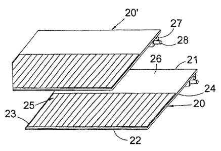
Referring to Figure g it is preferred that each element 20 is generally
rectangular
in form having parallel edges 21 and 22 intended to extend substantially
horizontally .
when the element 20 is placed in position on a roof, and having further edges
23 and 24,
also parallel to one another, intended to extend in the direction of
inclination of the roof.
The element 20 comprises an array of solar cells 25 integrally formed and
monolithically interconnected on an insulating substrate, each cell 25 being
aligned
perpendicular to the horizontal edge 22 and generally parallel to the inclined
edges 23
and 24. it will be seen that each of the cells 25 is elongate and extends over
the same
distance from close to the edge 22 over a proportion of the length of the
edges 23 and
24 leaving an area 26 of the element 20 which does not need to contain solar
cells. This
area 26 may be left blank ~s it will, when installed, be covered by the
adjacent row of
roofing elements 20.
Although other arrangements of the solar cells on the underlyring substrate
are
possible within the scope of the invention, the advantages of such an
arrangement will
be apparent by a comparison of Figures 6 and 7. Ln Figure 6, the solar cell
array
comprises a series of substantially square solar cells 30 arranged in adjacent
rows and
connected in series in the manner shown by the lines 31, with the cells 30
being
provided over substantially the whole of the area of the underlying substrate.
In this
case, as shown by the. rectangle 32, the overlapping element or elements of
the next row
of elements overlaps at least some of the cells 30, and thus prevents those
cells from
outputting an electrical signal {or reduces the magnitude of the signal where
the light
reaches the cells only at a lower light intensity). because the same current
flows
through all the cells in series and the current produced by each cell is
proportional to the
level of the incident light, the output current is restricted to the lowest
output of the
cells. If a cell is wholly in shadow so that it produces no current output, it
follows that
the whole series of cells will provide no current output. If a cell is
partially obscured its
CA 02480366 2004-09-02
7
output current will be reduced in proportion to the shadowed area, arid the
output
current of the series of cells will be affected accordingly.
By contrast, if all the cells 34 are elongate and arranged parallel to one
another,
as shown in Figure 7, whilst being connected in series as shown by the line
35, the
effect of any shadowing by overlapping elements as shown by the rectangle 35
will be
minimised. This is because such shadowing will tend to only partly reduce the
current
output of each cell, far example by a third, and, if all the cells are in
shadow to the same
extent, it follows that the output current of the whole array will be reduced
only by the
same amount. It is important to appreciate that any shadowing in elements in
building-
mounted systems is usually linear, since it is caused, for example, by
overlapping rows
of slates, overhanging eaves or other linear building features.
Referring again to Figure 8 each of the elements 20 and 20' shown therein
incorporates a rib 27, which incorporates an interconnection projection 28 for
engaging
within a corresponding recess in the end of the rib of an adjacent element in
order to
lock the elements together. This connection also automatically provides an
electrical
connection between the output cracks of the elements. Such an, element
incorporating a
thin film solar cell array may be substantially uni form in colour to provide
a close visual
match to natural and synthetic slates. The array is configured to provide a
peak power
voltage in excess of 20V and an open circuit voltage below 75V. The peak power
voltage exceeds 1 SOV per m2 of active solar cell area.
Figure 9 shows an alternative embodiment in which each of the elements 40 and
40' incorporates a monolithically interconnected solar cell array 43, and
oppositely
facing profiles 4I and 42 along opposite edges, such that adjacent elements
40, 40' can
be mechanical interlocked by engagement of the profile 42 on the element 40'
with the
profile 41 on the element 40. In this case the elements 40, 40' are broadly
flat in
construction, and provide interlocking mechanical connection of adjacent
elements and
preferably also protection against water ingress. The alignment of the solar
cell array
and provision for overlapping rows may be as in the previously described
embodiment.
CA 02480366 2004-09-02
_-
These embodiments allows particularly relatively high voltages per unit area.
No other products of the size of traditional tiles or slates achieve peak
power voltages
over 9V DG. For the reasons indicated above, peak power voltages in the range
2U to
120 ~' are most suitable. This embodiment allows peak power voltages over 2UV
and
particularly in the range 20 to 120V, It is expected that elements with peak
power
voltages in the range 20 to 75 volts will be of primary interest initially.
Additionally the
open circuit voltage is likely to be below 75 volts, that is at a safer DC
operating level.
Figures 10 and 11 show possible conf gurations for the electrical connections
within each element. Figure 10 shows electrical connection arrangements
suitable for
providing direct electrical connection between adjacent elements when such
elements
are mechanically interconnected. The electrical circuit shown at (a)
comprises'two
horizontal bus-bar rails 50 and 51, which effect the parallel connections
between
neighbouring elements. The conductive tracks 52 and 53 provide the contacts
between
these bus-bar rails and the positive and negative terminations of the solar
cell array 54.
The rails 50, S1 may be integral within the element as shown at (a) or in a
separate assembly attached to or ~ciose to the element as indicated by the
dotted
rectangle SS as shown at (b) in an alternative configuration. Similarly the
connections
to the solar cell array contacts may be within the element or made through a
hole in the
surface (or at the edges) of the element, as the indicated by the dotted hole
56 shown at
(b). The electrical connections between neighbouring elements may be formed by
any
suitable electrical, contact arrangement, such as malelfemale plug and socket
connections for example.
Figure I i shows electrical connection arrangements suitable for connection to
a
separate wining harness or bus-bar providing parallel connections bet~veen
elements. In
these arrangements the connections from the bus-bar rails 60 and fit to each
element by
means of the conductive tracks 52 and 53 are required purely to provide the
positive and
negative contacts to the solar cell array. These connections may be made
separately, as
shown at (a), or together, as shown at (b), and either at the edge of the
element, as
shown at (a), or by way of a hole 62 through a surface, as shown at (b). The
CA 02480366 2004-09-02
9
connections to the separate bus-bar or harness assembly may be formed by any
suitable
electrical contact arrangement, such as malelfemale plug and socket
coru~ections for
example.
The elements may be mounted on the building structure by a wide variety of.
means. Ideally similar methods would be used as are used to apply to standard
building
products, such as the methods described below with reference to Figures 12 and
13. 1n
Figure 12 the element 70 is shown mounted on a roofing batten 71 using nails
72 or
screws extending through holes 73 in the element. In Figure 13 a hook 7~ is
attached to
the roofing batten 71 and the element 70 is supported by the hook 7~ and
neighbouring
elements. Each element may be mounted by one or more than one of the mounting
means described.
The primary steps in the production of such solar building elements may be
carried out as follows. The insulating substrate 2 is prepared, either by
using a sheet of
insulating material, or by applying an insulating coating to a sheet of a
conductive- .
material, and is configured to an appropriate size and prepared for
processing. A
conductive contact layer is applied to the substrate 2 and configured in a
series of
separate strips. This may be achieved either by a process in which the
conductive layer
t~~~.4..~;
is deposited in sfrips' (such as by printing, or by deposition through a mask)
or by a
process in which the conductive layer is deposited as a continuous layer and
is formed
into strips by a subsequent processing sleep (such as by mechanical or laser
scribing, or
by etching) which removes thin sections of the layer. The solar cell
semiconductor is
then applied in contact with the contact layer, usually by sequential
deposition of three
sub-layers. In the case of multiple junction cells this sequence may be
repeated. As in
the case of the contact layer these sub-layers may be applied in separate
strips, or the
strips may be formed subsequently either to the deposition or to the
application .of the
second contact layer, for example by any of the steps described above with
reference to
the fabrication of the first layer. The second contact layer is then applied
in: contact
with the surface of the semiconductor layer. Again this second contact layer
is divided
into separate regions as described above leaving a series of narrow inter-cell
isolation
regions between adjacent cells. The relative alignment of these inter-cell
isolation
CA 02480366 2004-09-02
1~
regions provides the monolithic series connection beriveen the cells as
previously
described.
The element produced as described above is typically tested for electrical
performance before further assembly. It may be cut into several smaller pieces
Lo
provide a solar cell array suitable for the particular element, conveniently
for example to
match the size of a standard building product. The further production steps
may be
carried out in several alternative sequences, but typically include the steps
of attachment
of at least two output conductors to the solar cell array, attachment of
external
connection means to these conductors, laying up of the solar cell array with
other
components to achieve the desired final shape and size of the product; and
lamination or
other assembly process to secure the element as an integral unit and provide
appropriate
environmental and electrical protection for the solar cell array, the
conductors and other
components.
Various modifications of the above described embodiments can be contemplated
within the scope of tfe invention. For example the elements may employ mufti
junction
thin film solar cells arranged in the manner described and electrically
connected in
series. Furthermore the element may be configured to mimic a roofing tile or
panel, or
some other type of external building element, such as a building cladding
panel or a
building facade panel.