Note: Descriptions are shown in the official language in which they were submitted.
CA 02480407 2004-09-24
WO 03/081961 PCT/AU03/00365
X
XMPROYED DIMMER CIRCUIT ARRANGEMENT
TECkINICAL FIIr~LD
'FJ,vs invention relates to c7iz~cuit arrangements for controlling the power
provided to a
load and in parfiicular, to dimmer circuits far mntrohiz~g, for example, the
luminosity
of a light or the speed of a fan.
BACKGROUND TO TF~E TIVVENTi0~1'
Dimmer circuits are used to control the power provided to a load such as a
light or
eleckric motor from a power source such as maixis. Such circuits often use a
technique
referred to as phase controlled dy.nuning. This allows power provided to the
load to
be controlled by varying the amount of time that a switch connecting the load
to the
power source is conducting during a given cycle.
For example, if voltage provided by the powez source can be represented by a
sine
wave, then maximum power is provided to the load if the switch cannectixlg the
load
to the power source is on at all txrnes. In this way the, the total energy of
the power
source xs transferred to the lead. Tf the switch is turned off fox a portion
of each cycle
(both positive and negative), then a proportional amount of the sine wave is
effectively isolated froxxt the load, thus reducing the average energy
provided to the
load. For example, if the switch is turned on and off half way through each
cycle,
then only half of the power will be transferred to the load. Becau..Re these
types of
~circu3.ts are often used with .resistive loads cmd »ot inductive loads, the
effe~-t of
repeatedly switching on and off power will not be noticeable as the resistive
land has
an inherent inertia to it. The overall effect will be, for example in the case
of a light, a
smooth dimirung action resulting in the control of fine luxrunosity of the
light, '~'his
technique will be well understood by the person skilled in the art.
PCT/AU03/00365
~ ,a CA 02480407 2004-09-24
Received 18 June 2004
2
Such circuits usually consist of two parts, the first being a part to control
the rate of
rise of load voltage at each main half cycle. The second part is used to
control the
load current provided to the load via the use of a control switch.
Various means are used to synchronise the action between these two parts, some
more complex than others. Traditionally, the synchronisation is achieved by a
central control block which senses various parameters of the first part,
determines
when the second part should come into action and then upon such determination,
provides control signals to the second part to control the switch. This
circuit
configuration is somewhat complex, both in design and implementation.
In devices that are mass produced, simplicity of design can lead to
significant
savings in cost during manufacture and an increased reliability in the
function of
the final product.
Similar considerations to each part of the circuit also apply and any
simplification
to any of the circuit blocks can lead to similar benefits.
Accordingly, it is an object of the present invention to provide a dimmer
circuit
arrangement which results in a simplified design.
SUM1VIARY OF THE INVENTION
According to the present invention, there is provided a dimmer circuit for
controlling the delivery of power to a load, the dimmer circuit including: a
first
control circuit for controlling a first switch for controlling a rate of rise
of voltage
across the load; and a second control circuit for controlling a second switch;
wherein said second control circuit is controlled by said first control
circuit.
Preferably, the first switch and the second switch are separated by a
rectifying
circuit.
:o
~~'-~,~~a'~=l~~~t ~~~
1~ ~~~/~~~
PCT/AU03/00365
CA 02480407 2004-09-24
Received 18 June 2004
3
Preferably, the second control circuit is controlled by said first control
circuit via the
rectifying circuit.
Preferably, the second control circuit obtains control signals from the first
control
circuit by sensing a voltage across said rectifying circuit.
Preferably, the second control circuit is actuated upon sensing that said
voltage falls
below a pre-set voltage threshold.
Preferably, said pre-set voltage threshold is determined by a zener diode.
Preferably, the pre-set voltage threshold is set to exceed a conduction
voltage level
of said first switch.
Alternatively, the second control circuit obtains control signals from the
first
control circuit by sensing a current through the rectifying circuit.
Preferably, the second control circuit is actuated upon sensing that the
current rises
above a pre-set current threshold.
Preferably, the first switch is an IGBT power semiconductor.
Preferably, the second switch is a triac.
Preferably, the second control circuit controls the second switch to control
the load
current provided to the load.
Preferably, the dimmer circuit is a leading edge phase control dimmer circuit.
-~~w~~.~~~~!~~~.~' ~;a~E~
D~,~'~1~a~9
CA 02480407 2004-09-24
WO 03/081961 PCT/AU03/00365
BRIEF DESC1~TON OF THE DRAWINGS . .
Figure 1 shows a first embodiment of the dinuner circuit of the present
invention;
Figure 2 shows an alternative arrangement of the triac control circuit portion
of
Figure 1; . .
Figure 3 shows a current switch control circuit which may be used as an
alternative
to the voltage switch control rireuiit of Figures 1 and ~; .
Figure 4 shows a simplified block diagram of the circuit of Figure x; az~d
Figure 5 shows an alternative aTxangexnez~t fox the impedance load imbalance
detector portion of Figure 1.
DETAILED DESCRIPTfON OF'~iE PREFERRED ~D'
A, preferred circuit design of a 2-wire, leading edge phase contxol light
dimmex~/fan
speed controller is shown in figure 1. The design shown in figure 1 is
particularly
effective in that it is electroxnagzietic compatible (EMI coizxpliant). 'This
zefers to the
amount of elertromagxxetic anterferez~ce (EMI) that is generated by the
circuit. The
amount of ~radiafiion generated by dimming circuits due to the high frequency
switching of the circuit is heavily zeguJ,ated and such circuits must xtot
exceed the
regulated level of EMI.
'Ihe cixcuit design of figure 1 cozttrals the level of EMI generated by the
circuit via
active control of the rate of rise of load voltage at each main half cycle. A
power
semi.condtictor in the .~orn, of an IGBT is used for this ftmction. 'ihe
IC:iST arci
associated dive control circ=uitry is eormec~ted to the DC side of a diode
bxidge to
allow contzol of polarities of mains voltage.
.A power txiac is used tv haxtdle the load cuxrez~t once the IGBT has
performed the
reqt~ared slow switchizvg function. This reduces power dissipation to a
minimum
since it has an ox~-state voltage lowez than that of the IGBT/bridge
conduction
voltage.
CA 02480407 2004-09-24
WO 03/081961 PCT/AU03/00365
Tkte IGBT circuit of figure I can be separated into the following blocks:
- low voltage DC powez rail
- nnain voltage zero cross detector
- power up drive inhibit
- control timiztg
IG13T gate drive
Power for the IGBT control circuit is derived from mains via the load, in each
half
cycle during the time peziod before IGBT operation commences, ie. while
znaiz~s
voltage appears across the dimmer. overall current consumption i.s long enough
to
allow the use of a relatively low dissipation resistive chavn provided by RI,
R2, R~ .
and 1t5. A smoothing capaator, C9 stores enough charge provided at the start
of each
half cycle to provide circuit current ,for the remaining period, with
relatively low
ripple voltage. Fxcess supply current is shunted by voltage regulating xener
diode
D,Z1 with the .resultant of nominal L1C power rail of 15 volts. 'This
arrangement
provides the low voltage DC power rail block referred to above.
The mains voltage zero acoss detector resets th.e control timing cixcizit
(described in
more detail below) in each half cycle after load curz~enfi coxxrnez~ces.
Timing is
allowed to start again when mains voltage reappears across the circuit in the
fc~llowin~ half cycle. For resistive loads this will correspond to mains
voltage zero
crossing. por .indu.ctive loads however, this corresponcLs to load cw.-remt
zero
crossing, which occurs later than maims voltage zero crossing.
Transistor (~2 with its emitter coruiected t4 th:e DC rail, has its base
driven by the
power supply voltage dropping resistor chain described above. The collector
pulls
"sync" high. whenever the voltage across the dimmer circuit is below the DC
rail
voltage. Conversely, when mains voltage exists across the dimmer ci.~cuit,
transistor
Q2 base emitter junction is reverse biased, preventing the collector from
pulling up.
CA 02480407 2004-09-24
WO 03/081961 PCT/AU03/00365
6
During this time supply current is delivered to the DC rail via base~emittez~
shunting.
diode T54 .
Reset of the controlled tizivng capac~tvr C7 is performed by discharge
transistor Q12,
which is driven by limiting resistor R2J; from "sync' output of Q2. Transistor
Q12
has base-emitter bypassed resistor R22 and capacitor C6 to reduce off-state
leakage
and to enhance EFT immunity.
The function of the power up drive inhibit black is to inhibit the operatioxi
of the
dimmer arcuit fox the first few main half cycles at power'-up by temporarily
by-
passing the control timing capacitor C7 charging current. This is requixec~ to
enable
correct operation of the soft-start mechanism, which relies on an established
DC
voltage reference to function. A. small capacitor C1, effeckively connected to
the DC
rail, provides a current via diode D3 to drive discharge transistor Q12 during
the .
period while the rail is rising at power-up. Blocking diode D3 isolates Cl,
from Q12
drive circuit once C1 has become completely charged after the power-up event.
Resistor R8 thereafter serves to hold C1 in the fully charged state, in
addition to
providing a discharge path at power off.
Tkte control tirx~ing block is used to provide the dirxune~r circuit with
immunity to
mains voltage ripple injection.
At the start of each maix~R half cycle, tizxwlg capacitor C7 charges via
mains/loacl.
through current limiting resistors R6 and R7. A reference voltage
deterznined.by
zener diode DZ4, sourced by resistor R39, is used as a charge threshold level
for
ternr~inating the txmix~g process. The voltage on the positive side of C7 must
always
reach a level of approximately two diode drops above. this reference level, as
determined by series connected diode D5 and transistor Q~, in order to
ixvtiate IGBT
operation. At the pre-defined threshold voltage, the timing capacitor
chaxgizlg
current is diverted to transistor Q4 in order to operate the IGBT drive
control stage.
CA 02480407 2004-09-24
WO 03/081961 PCT/AU03/00365
7
,Adjustment of control firing angle is facilitated by a variable control
voltage source
connecting to the negative side of the timing capacitor. This control voltage
is
dexived front zener diode DZ4 referenced voltage using z~naizv dinnrner
controX
potentiometer VR~. An RG filter made up of IBS and C~~ pxovides a soft-staxt
feature at power up due to the zero initial capacitor voltage condition.
Buffering of
the filtexed control voltage is perfox~ned by cascaded transistors Q3 and (~15
to
laz~ovide a low impedance source voltage. Resistor R36 bypasses the
base~eznitter of
transistor Q1,5 to xeduce leakage effects.
.At the maximum control voltage (for ma3dmuxn dimmer conduction angle), she
required timing capacitor chaxging voltage is at its lowest. The nvnixnun~
required
tinning capacitor chaxging voltage is equal to one foz ward voltage diode
drop, as
detenx~ined by diode D5, in addition to a small voltage across resistor R11.
This level
is independent of the absolute value of the zenex diode DZ~ reference voltage.
Conseduently; the maximum conduction angle is inherently limited, being
largely
independent of component paran;~etez~s, thus ensuxing sufficient current is
always
available to supply the DC rail. Resistor 1211 is included to further restrict
the
maximum dimmer conduction angle.
I'TC1 is placed in series (on the reference ~~oltage aide) with VRl to provide
ai~ontatic :ea~:ction of conduction anr~le in the event of dimmer oven-
temperature
due to over loa.dW g of klle product. Trimpot VR2 is placed in series
(cixcui.t comrzzon
side) with VRl to allow adjustment of the minimum conduction angle, by raising
the
rx~ininnum control voltage.
The IGBT ,gate dzive control circuit is provided by transistors C~1.6, Q17 and
Q5. The
cixcuit behaves as a non-retxiggerable monastable and provides controlled gate
drive
current to the IGBT to achieve the desired slaw switching outcome. Transistor
Q5,
connerked to the DC rail, acts as a switch to source TGBT gate MlTxent via
tizxvng
CA 02480407 2004-09-24
WO 03/081961 PCT/AU03/00365
8
resistor R38 at turn on. Transistor Q17, connected to circuit common, acts as
a switch
far rapid discharge of 1GBT gate charge at turn off. .
Base drive current for input transistor Q16 is sourced by Q4 from the control
tinning
circuit. The base-enuttex is bypassed by resistor It27 and capacitor C4 to
reduce off .
state leakage and to enhance ElI' immtuiifiy. When transistor Q16 is not
dxive~n,
transistor Q17 is suffiiciently biased vi,a resistors 1t,3, R13, R35 and R48,
so that the
collector holds the IGBT gate an the discharged (off) state. In this
rnndition, transistor
Q5 is not suf~riently biased to operate. When traz~istor Q16 is driven,
resistor R35
provides sufficient bias to operate transistor t~5, which provides temporary
regenerative base drive fox transistor (,old via RC network R37 and C8..7.'his
result in .
monostabie action (approximately 300 micro seconds output dlixafiion). IJuring
this.
active condition, bias is removed froze transistor Q17.
The combination of 1GBT series gate current linnitizig resistor 1238 and
parallel gate
capacitor gate C14 provides the required slow turn-an characteristic fox EMC
control
at IGBT turn on. The values selected are specifically suited to the ZGBT used,
in this
case 1RG~ 13C20S.
The triac control circuit xs shown in figure ~ in the circuit block on the A,C
side of the
:Node bridge. The primary function o.f this circuit is to trigger the triac
Q23 once the
1GBT has completE.d the slow-switching EMC emission reduction operation, can a
pe.r
half-cycle basis. .An essentially syzimetrical circ~ut is used to provide a
friar gate
drive pulse nn quadrants 1 and 3 (gate drive polarity follows mains polarity).
Additional functions performed by the friar control circuit include over-
~ciurent
protection and dinnznez over voltage protection. Either of fihese conditions
result in
mediate friar tsiggexing. During over-current conditions (for example
incandescent inrush current), the friar shunts current away froze the 1GBT.
Durrxig
CA 02480407 2004-09-24
WO 03/081961 PCT/AU03/00365
9
ever voltage conditions (for example maixis transients), the trice shunting
action
tzansfexs the transient potential to the load. _.
The friar control circuit derives its power from the mains via the load, ix1
each half
cycle during the time period before IGBT operation com~x~ences, that is white
mains.. ,
voltage appears across the dimmer. Average current cox~sut'x~ption is long
enough to
allow the use of a relatively low dissipation resistive chaixl made up of R16,
R17, R1,8
and R19. During each mains half-tyde, current provided by the resistor chain
is used
to charge the capacitor C10 to a voltage with polarity determined by the
mains. The
voltage developed across capacitor C10 is limited to approximately 20 volts
~or each
polarity, as defined by shunting zenex diodes DZ2 and D7J3. The sequence of
operation of the drive circuit ~or each half cycle polarity is as follows:
reservoir capacitor C10 is charged while mains voltage is present.
A 100 micro second time delay circuit (RZ~ and C3) is initiated after the
dimmer voltage falls below approximately 20 volts due to TGBT operation: .
At the end of the time delay, the trice (,~23 gate is supplied with current
from capacitor C10 via limiting resistor R41.
Tn the positive mains half cycle, reservoir capacitor C~ O is charged to
appxa~dmately
20 volts from zoains through limiting resistors R16, R17, R~8 and R7,9 vi,a
the base-
emitter jtu~ction of transistor Q18. When dimmer terminal voltage drops below
the 20
~~nlts at threshold, transistor Q6 provides charging current via currezlt
limiting
resistor P~24 fox tinne-delay capacitor C3. When the voltage across capacitor
C3
reaches approximately 0.6 volts, transistor (~13 operates, which in turn
provides
basic current drive for output transistor Q1 via current limiting resistor
R10. Some
xegexzerative feedback ~(xorn the collector of transistor Q2 to the base o~
transistor Q1,3
via resastox R12 speeds up the switching acdori. The collector of transistor
C?1 drives
the trice gate via steering diode D'7A and gate current limzting resistor R41.
The
function of diode D7A is to isolate the trice gate caxcuxt dozing charging of
reservoir
CA 02480407 2004-09-24
WO 03/081961 PCT/AU03/00365
capacitor C10 during the negative half mains half rycle. Thus is necessary
because the
base-collector junction of output transistor Q1 is forward biased in this
period.
Capacitor C3 has the additiv~nal role of enhaztcxng Ek'T immunity fax
transistor Q13,
while resistor R2~ reduces transistor leakage. Siznilaxly, resistor R9 reduces
leakage
of output transistor Ql. which would consequently affect the C3 timing period.
The operation of the circuit for the negative mains had cycle is the same as
described .
above but uses. the mirrored set of components.
Applications utilising isolated PWM control ~or dimixting level require that
bath the
ZGBT (Q22) and triac (Q23) together with associated drive arcuitry is
pemnanently
connected to zx~ai~n.s. This differs from the manually controlled two-wize
modular
dirnxner application where a sezies mains interrupting switch is always used
for load
on/off control.
Generally in the dimmer circuit design, triac fixing operation commences as
the
dimmer texmi~ial voltage falls below a threshold level as a consequence of
IGBT
operation.
A modification to this method of operation is zequired fox the isolated
control
interface ci..imoef which has pexrnax~ent mains connection. In this case it is
necessary
to disable triac triggering which would otherwise be initiated near the elld
of ezrery
mains half cycle. Although the load is effectively in the off state, due to
the very low
prevailing triac conduction ax<gle and hence load voltage, the resulting line
conducted EMC emission levels would be quite large due to such triac
operation.
To address this situation, additional circuitry has beezt incorporated which
differexitiates between the rate of change of maim voltage due to IGBT
operation
CA 02480407 2004-09-24
WO 03/081961 PCT/AU03/00365
l.1
during diunnmiz~g, and that due to normal z~nains voltage waveform when the
~IGBT ~is
not ackivated via the isolated control interface.
It: diznming operation, the triac drive circuit is normally disabled and is
ooiy enabled
fox a shoz~t period after detection of the relatively fast rate of change of
load ternvx~ai
voltage due to IGBT operation. Durax~g load off state conditions, the triac
drive circuit
is not enabled by the relatively slow rate of fall of mains voltage near the
end of each
half cycle.
Some important design considerations for this additional caxcuitry are that a
high
irru~nunity to mains transients and mains ripple control signals is
maintained.
1?xgure .2 shov~rs a nnadified circuit of the triac control circuit of Figure
1 as described
above, in which coxnrnon elements axe identified accordingly.
,Ps descxiptioz~ of carrcuit operation with reference to Figure 2 for one
mains half cycle
polarity follows.
A damping transistor, 'x,.7300 is used to disable the friar drive circuit from
operating
by shunting the charging Current for the txiac fixixtg time delay capacitor,
C3. A filter
capacitor, 0300 is noxm~~lly charged from the tZOV rail via resistive divider
elements,
8300 & 8301 with such polarity as to maintain the bias to tile clamping
transiys'to~.
During IGBT, X22 operation, the resulting bridge voltage dv/dt praduce,.~~
suffiaent
Current through a small mains coupling Capacitor, C301. to rapidly discharge
the filter
capacitor ixt vrdez to reverse bias the clamping transistor base-e~azit~ter
junction. The
cJampixtg traxisistor remains biased off lung enough to allow normal chargzng
of the
triac firing time delay capacitor, due to the filter capacitvr/bi.as resistors
time
constant.
CA 02480407 2004-09-24
WO 03/081961 PCT/AU03/00365
Tmmunity to maps ripple iinjection is achieved through the love pass-filter
action of
the capacitor and bias resistors.
Without IGB~' operation the relatively low dv/dt associated with the rnaix~s
voltage
waveform xs insufficient to remove the bias voltage on the filter capacitor.
'xhus the
clamping 'transistor continues to bypass ch,axging of the triac bring delay
capacitor,
preventing possibility of triac aperatidn.
A. series resistor element, X302 for the mains coupling capaator provides
current
Jaxniting protection under mains suxge/transxent conditions.
A reverse connected diode, D300A is required across the colX.ectvz-emitter
junction of
the clamping transistor, ~3Q0 un order to prevent the transistor frorxt
interfering with .
correct operation of the associated transistor, Q301 in the opposite half
cycle. In
opposite half cycle, the collector-base junckion of (,~3p0 becomes forward
biased and
can source sufficient bias current to operate the associated transistor,
(,301. The
parallel diode, D300A works by limiting the collector voltage to only one
forward
diode drop, therefore limiting base drive voltage fox associated transistor,
Q301 to
approx. zero volts.
The above voltage driven triac control circuit may equally be replaced by a
current
driven triac control circiut as shown ixt figmre 3. Once agavz, the prinZ~ry
fun~~ticm o.~
this circuit is to trigger the triac once the IGBT has completed the slaw-
switching
FMC emission reduction operation, on a per half-cycle basis. The eircuit is
essentially
symmetrical and is used to provide a triac gate drive pulse in quadrants 1 and
3 (gate
drive polarity ~vllows mains polarity).
In operation, a current sense resistor,1~32, is used to derive dzive potential
far the
entire triac drive circuit. After a defined load current threshold is
achieved, sufficient
for triac gate requirements, excess current is by-passed by sexier connectlztg
diodes
CA 02480407 2004-09-24
WO 03/081961 PCT/AU03/00365
13
D3 and D4. The developed sense voltage begins charging a tune delay network
n'~ade
up of resistor R33 and capaator C9. A comparxtvr transistor, Q14, is driven
via
resistor R35 once the txnung arcuit output voltage reaches a threshold level.
This
level is determined by the voltage at the junction of voltage divider
resistors R34 axed
R37 (souxced by the initial sense voltage), in addition to the base-emitter
junction
voltage of transistor Q14,
The operaBon of traz~sistox Q14 results in simultaneous application of base
drive for
transistors Q10 and Q11, via respective base current li~ti~ting resistors R26
and R28.
Traxlsistox Q17,, referenced to the sense voltage, proceeds to drive
transistor Q15 via
resistor R36. Qperation of transistor Q~.5 reduces the comparative threshold
voltage
by lowering transistor Q14 ennittex potential. This positive feedback process
is
regenerative to speed up the switching action. The application of the triac
gate drive
current is via output transistor Q7.0 and current limitixtg resistor R41.
Resistors :R27
and R38 axe required to prevent possible adverse effects from leakage axtd
trarisi,stors
QJ.O, QL3. anal Q15.
The operation of the circuit for the negative mains half cycle is the same as
described
above, using the nr~irroxed set of con~ponextts.
During IGBT over-current conditions, sufficient voltage is developed across
current
sense resistor R40 to bias on traniqistor Q18. This in turn provides b~~.se
curresit drive
for upward transistor Q10, irnxnediately operating the triac, to divErt
current away
from the IGBT circuit. Resistor R39 limits transistor C,~18 ba.se current
drive to a safe
level under these conditions. This provides an inbuilt circuit protection
meclZanism,
At dimaner aver-voltage currents, the triac gate is directly drzven by series
connector
txanzorbs BZ1 and BZ2. Capacitor CIO is placed across the triac gate-MTl
ternvnals
iz~ order to enhance the txiac immunity to dv/dt triggez-ing froxx~ mains
transients.
CA 02480407 2004-09-24
WO 03/081961 PCT/AU03/00365
Tnductvz~ L1 limits the zate of transfer of lead curreant from the I~BT
circuit to the triac
on order to . control line conducted »I emzssivx< levels. The amount of
inductance
required fox this function is related to the difference between the triac on-
state
voltage and the voltage across the IGBT circuit current above just prior to
txiac
operation, The presence o~ cuixent sense resistor R32 in the IGBT circuit
current path
introduces additioxtal voltage differential, there by iaifluencir~g the amount
of
inductance redrxired. An additional means o~ controlling line conducted EMI .
emission levels us via shunt capaator C11 which works in rnnjunction with L1
to
form. a second order low-pass-filter.
A particular advantage of the present circuit is the ability of the triac
control circuit
(whether it would be voltage driven or current driven;) to be cor<trvlled
directly by
the ZGBT circuit rather than vita a third centralised control block as in
prior systems.
In the case oaf the voltage driven drive circuit, this essentially mozvito~rs
the diode
bridge voltage, ~undex control of the Qperational IGBT in order tv determine
when
triac firing should occur. The necessary charge required for triac gate drive
is
accumulated .from, the available mains voltage ion the period of the halfrcyde
before
comrxlenceznent of IGBT conduction. The triae is essentially fixed wheat the
diode
bridge voltage is reduced below a minimum set threshold. 'This minimum set
threshold is determined by zener diodes DZ2 and I7Z~3 which in the present
example,
said a n~ininzum threshold. of 20 volts (for the positivE rzn.ci negative
cycles j. The
voltage at the diode bridge is sensed by traxisistor Q6 and resistor network
R17, R~6,
R18 and R19 as would be understood by the person skilled in the art. The
minimum
voltage threshold is determined by the componez~ts used (in this case the
xener
diodes DZZ axed D,Z3) az~d is generally set to exceed by a suitable margin the
conduction voltage for the IGBT a.rcuit. -
In the case of the current driven drive caxcui.t, this essentially monitors
the diode
bridge current under control of the operationaX IG13T, zn order to deterl~lrte
when
CA 02480407 2004-09-24
WO 03/081961 PCT/AU03/00365
triac firing should occur. The necessary current required for triac gate drive
is
derived from the load current resulting at IGBT conduction in the half cycle.
,Agaix~
the tniac is fired when the diode bridge current vises above a minimum
threshold
which in this case, is set by resistor R32.
In this way, the circuit configuration is far simplex than prior art designs
which
require a separate centralised control block monitoring electrical parameters
of the
ZCBT circuit, detexmi~ng when the triac should be fired in relation to those
semsed
parameters and providing control signals to the ~triac control tixcuit.
Alternatively,
the centralised control black sornetames provides control signals to both the
IGBT
az~d triac control airc~its independently of each other, based oz~ pre-set
timing
parameters.
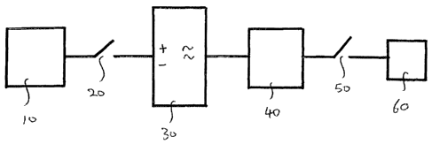
,A, simplified block diagram of this circuit arrangement is shown in Figure 4,
ix~ which
element 1.0 represents the first control ciurcuit (rGBT control), element 20
represents a
first switch {ZGBT), element 30 represents the rectifying circuit (eg. Diode
bridge),
and element 40 represents the second control circuit (txiac ~Qntrol), which
obtains its
control signals from first control circuit x0, via rectifyixig circuit 30.
Element 50
repzesents the second switch (triac), which is controlled by second control
circuit,
and element 60 represents the load.
W practice, th.e voltage driven triac clrivem control c:ixcttit is preferred
over. the cura~ent
driven tziac drive circuit. However, each has advantages and disadvantages.
'Ille
voltage driven txiac drive circuit allows minimal size of EMC filtez~
components
which results in highest overall product efficiency. The voltage driven
circuit
however requires voltage dropping elements to derive a power source from the
mains, therefore introducing local powez dissipation problems (only at low
conduction angle seriings, where total overall dissipation is low). Further
more,
additional components are required to disable the txiac drive when no IGBT
drive is
CA 02480407 2004-09-24
WO 03/081961 PCT/AU03/00365
16
present to achieve off-state conditions (only reduixed fox applications
without series
manually-operated switch).
In contrast; the current driven accost does not require a power source
connectiion to
fhe mains, axed therefore no local power dissipation issues are encountered.
Further
mere, the triac drive is one hundred percent disabled when there is no XGBT
drive to
achieve the of state (this is an advantage only for application jn~ithout a
series
manually-operated switch). The current drive circuit hawevex suffers from the
disadvantage that the presents of current sense companents necessitates
large~z EMC .
filter components, and lower overall efficiency is achievable.
,Another circuit block provides circuit protection froth over rurrezit
conditions which
may arise from 1GBT operation. Ihuing such conditions, sufficient voltage is
developed across current sense resistor R42 to bias on transistor (,~14. This
in turn
provides base current drive for output transistor ~1, immediately operating
the triac,
to divert cmxent away from fhe zGBT circuit on the DC side of the diode
bridge.
Resistor 1,140 lizz~its transistor (,~24 base current drive to a safe level
under these'
conditions.
At dinuner over-voltage occurrences the txxac gate is diarectly drivers via
series
connected tranzorbs Dl and z72 and current limiting resistor RZO. Capacitor
C~1 is .
placed across the triac gate MT1. terminals in order to enhaxlce the triac
immunity to
dv/dt tziggering from rc,ains transients.
In this dimmer design topology, it is not necessary to incorporate an inductor
to
achieve the required RF emission level lixruts. A relatively small inductor.
may
however by required to provide some degree of di/dt protection for the triac
during.
TGB~' over current conditions. In normal. operation, the voltage appearing
across the
triac just prior to firing is of the order of a few volts, depending on the
achial lead
current rnagni,tude. This voltage is a huiction of the IGBT saturation voltage
and
diode bridge forward voltage characteristics. At such low operating voltage
levels,
CA 02480407 2004-09-24
WO 03/081961 PCT/AU03/00365
7
the triac switching action is more gradual than zn standard high voltage triac
applications. This results in an inherent smooth transfer of current from ZCBT
to the
triac, with low associated RF enZission levels. 'The addition of the inductor
L1
however, slightly increases the RF emission cornponez~t associated wrath
transfer of
current fronn the IGBT to the triac. This corresponds to the small ixttroduced
current
wave form discontinuity at the ~ou~t when the IGBT torrent drops to zero.
Additionally, at the end of each mains half cycle wvhere the triac naturally .
.
comnnutates off, a burst of I~ exnxssion occurs, due to the discontinuity in
the load
current wave form. Attenuation of this emission is achieved by a capacito~r~
C1.5 place
across the dimmer terminals. Azi important additional role of this Capacitor
is in
ionproving tlxe entire dimmer circuit imzxiunity to EFT.
Another circuit block is an inductive load unbalance detector. The function of
the
circuit block is to shut down dxmme_r control in the case of excessively
asymmetrical
operation, which znay be the result of connection to an uriloaded iron-core LV
lighting transformer. l7~nvng operation is suspended if the average voltage
acx4ss
the dimnner terminals fox the positive az~d negative half cycles are not
similar.
lzeferz~ing back to Figure 1, two resistor divider chains made up of resistors
R4.3, R44,
R29 and R45. ~L46 aztd R30 are used to sense the mains voltages appearixtg at
the
active and load termixvals respectively. When referenced to the bridge common
(ne,gative) terminal, these voltages represent opposite polarities of the
mains voltage
across the dilxuner. The divider junction of each chain is connected to
opposite sides
of capacitor C~2, to produce a differential voltage proportional to the
difference in
half cycle voltages. 'T'wo t7ransistors, Q9 and Q10 are used to produce a
common-
referenced signal tf the differential voltage exceeds a threshold of
approximately 0.&
volts. A latch curcuit made up of transistors Q11 and Q20 and resistors R3~
and R34
has input driven by the imbalance detector output. A transistor Q21, wired as
a low
CA 02480407 2004-09-24
WO 03/081961 PCT/AU03/00365
Z8
leakage diode, directs latch output fronn tra;naistor (~J,1 cohector to
"syxtc", ie, to drive
the timing control bypass transistor (~12.
Transistor Q21 arts as a blocking diode to prevent any latch operation by the
zero
crossing detector. Base-ez~ittex bypass resistors R31 and R33 are required to
nr~iniuvse
leakage in the respective transistors. Similarly, capacitors C5 and C1.6 are
present to .
enhance EFT nmmwnity of the latch circuit. >'n addition, capacitor C5 provides
rejection fox any high frequency signal. component from the unbalanced
detector
output.
When operating inductive Loads, the dirxlmer circuit incorporates a modezately
sensitive triac assist in achieving an acceptable level of performance,
particularly in
terms of operating syznmetzy with worst case load types, ie. low value VA,,
highly
inductive loads such as exhaust fan motors.
In normal dimmixig operation, the IGBT i_nifiial~y operates followed by firing
of the
txiac after a fixed time delay. lhuring this pre-txiac conduction delay tune
period, the
inductive load curreztt has an opportunity to develop in magnitude. This delay
time
therefore also increases the ability of the triac to operate successfully with
such
difficult loads.
At very low conduction angle settW gs however, there znay 6e insufficient load
c,_rrrent available for reliable txiac latching. In this case, a low level
load, DC
component will be Sustaiz~.ed by the dimmer in combination with the non.-
linear load .
inductance. Under these conditions; there is no danger of damage to the load
due fo
the relatively low rrns current magnitude. If Load DC component levels become
excessive operation of the imbalance detectoz will automatically shut down the
dimmer control.
CA 02480407 2004-09-24
WO 03/081961 PCT/AU03/00365
19
In general, capacitive input electronic LY transformers are not generally
suitable for
leading edge pln~se cantzol diu~mexs owing to the additional resulting dimmer
power dissipation. Tk~e high capacitor charging torrent pulses increase line
conducted EMC emission levels and nnay produce repetitive high frequency
rx~ging
bursts on the mains voltage wavefoxm., .
The dimmer circuit of figure 1 incozporates loadwer current sensing applicable
,
during the IGBT canductioz~ period. Ain~ner connection to such capacitive
loads
result in sustained operation of the over-cwrrent mechanism, producing even
higher
EMC emission levels. In addition, the high frequency and amplitude ringing
current
wavefoxxn which typically present for the flurst few hundred micro seconds
xnay
result in conunutation of the triac. If this condition prevaitls, the
iuu~alanced protector
znay cause the dzxnmer control to shut down. For electronic transformers with
maximum rated load connected, this condition is far less likely to occur.
Axe alternative circuit configuration far the inductive load ixxibalance
detector of
Figure 1 as described above is now described with reference to Figure 5, which
shows an alternative circuit arrangement for the ZGBT control of Figure 1.
The general operation of tk~e imbalance deterkion process is described as
follows.
A capacitor, used to represent conduction time, is repetitively charged fzom
zero to a
level detexniined by the prevailiry izalE cycle cc>nduction period. The
voltage
de~Teloped on this "conduction. time detection" capautar is used to set th.e
peak
voltage on a second capacitor, to represent peak conduction tune.' This "peak
conduction tune" cap~citox is simultaneously discharged with a constant do
current
sink. The resulting "peak conduction time" capacitor voltage wavefo~rm
comprises
hnro components. (~.) A do component exists with magnitude proportional to
half
cycle conduction period. (2) An AC component exists in the form of a sawtooth,
with
magnitude determined by fixed paratx~eters ie. capacitor value, magnitude v.f
do
current sink and repetition frequency (2 x majxts freq.).
CA 02480407 2004-09-24
WO 03/081961 PCT/AU03/00365
2p
If su~ieient difference in alternate polarity half cycle conduction periods
exist, the
xesultixig AC voltage wave~orm associated with the "peak conduction time"
capacitor has double the normal amplitude, at only half the repetition
heciuex~cy
(rnairLS ~xeq.). A simple amplitude threshold detector, with do blocking
properties, is
used to activate a latching circuit in order to disable dimmer operation when
the
condition is detected as a steady state.
A more detailed description with reference to actual components involved
follows:
During load conduction period o~ diznnvztg cycle, transistor Q2 collecto~r~can
source
current via limiting resistor 8203 to "conduction time detection" capacitor
0201.
When dixr~mer reverts to the non-conducting state, at the ex~d of each half
cycle,
diode D200 isolates az~y current associated with charging of mazn timing
capacitor
C7.
Transistor X7200 is used to reset C20i. to zero volts at the start of each
half cycle
conduction period. Associated pulsed base drive for t~200 is provided by
capacitor
C200 in series with resistor 8201. Diode D201 in conjunction with resistor
iZ200
provides the necessary discharge path for C200 in preparation for next mains
half
cycle event. Resistor 8202 bypasses base-emitter of (,200 tv reduce device.
off-state
leakage, during charging period of 0201.
Transistor Q201 is coWi.gured as un emitter follower, so that the voltage
across
capacitor 0202 must Follow the peak voltage of C201, dua~ing brief period
where
(~201base-eznittex input is Forward biased. Traxtsistar Q202 nzi eonjunctioz~
with bias
resistors R20~k, 8205 & R20b is configured as a current sink fox C202.
The sawtQOth voltage waveform across 0202 is AC coupled to flue base of
"threshold
detection" transistor X203 via diodes D202/D203 and capacitor ~C203. Series,
connected dzode D203 functions to provide enough sigxal voltage drop so that
0203
is not driven under symzneizical dimmer operating conditions, where input
SigTtal..
CA 02480407 2004-09-24
WO 03/081961 PCT/AU03/00365
2I
amplitude is normally low. Resistor 8207 reduces Q203 device off-state
leakage, iri
addition to providing a reverse charge path for C203. Diode D202 also forms
part of
the reverse charge path fox 0203.
Under asymmetric dimmer operating conditions, Q203 is operated in pulse mode,
'at
a low duty cycle. An RC network comprising 8208 and 0204 is 'used to provide
ari
averaging function for the resulting pulse train. Transistor Q204 forms part
of a latch
circuit, which is triggered When the voltage across 0204 reaches a critical
level - as
defined by voltage divider resistors 12209 & 8210 in conjunction with Q204
base-
emitter threshold potential. Transistar Q205 in conjunction with resistors
R2~1& 8212
forms the xemairung part of the latching circuit.
At maims power-up or at initial activation of 1?'VVM dimmer control drive, it
is
necessary to ensuz~e that the latching circuit is cleared to the unlatched
state for a
number of complete mains cycles. This function is performed by RC network
comprising 8213 and 0205, which initially holds the base drive voltage for
Q205 at a
level less thax~ the emitter reference level.
It will be appreciated that the above has been described with reference to a
preferred
erx~bodiment and that many variations azid modifications axe possible as world
be
understood by the person skilled in the art.