Note: Descriptions are shown in the official language in which they were submitted.
CA 02480920 2004-09-09
IC CHIP FOR IDENTIFICATION, DATA-READING METHOD,
AND DATA-WRITING METIiOD
BACKGROUND OF THE INVENTION
1. Field of the Invention
This invention relates to an IC chip for wireless identification that is used
for identifying various types of objects, persons, and the hike, and to
methods for
reading and writing data from/to the IC chip.
This application is based on Japanese Patent Application No. 2003-319280,
the contents of which are incorporated herein by reference.
2. Description of the Related Art
Many kinds of IC cards and IC tags have been developed, and they are
widely used for identifying various types of objects, persons, and the like.
IC
cards and IC tags may be contacting or non-contacting, but the non-contacting
type that incorporates an IC chip for wireless identification is superior,
since it is
more convenient to use. In addition to incorporating the wireless IC chip in
an IC
card or an IC tag, it may be incorporated directly in various types of
objects,
including paper money and the like, and used in identifying them.
A conventional wireless IC chip for identification supplies electrical
power by using carrier waves from the outside (e.g. see Japanese Unexamined
Patent Publication No. 10-145443). That is, when carrier waves from an
external
reader/writer are received via an on-chip antenna, they are rectif ed to
create an
internal power source, so that data that has been superimposed an the carrier
waves can be read, and the required data can be transmiti:ed by radio.
CA 02480920 2004-09-09
According to the conventional art, carrier waves from the outside are used
not only in creating an internal power source for the IC chip but also as
carrier
waves for carrying data; one problem is that, in order to accurately
demodulate
the superimposed data, the carrier wave frequency must be kept constant, which
tends to limit the range of application. That is, since the characteristics of
the on-
chip antenna mounted on the IC chip are affected by the properties of the item
that incorporates the IC chip, fixing the carrier wave frequency makes it
necessary
to adapt the characteristics of the on-chip antenna to each individual item.
SUMMARY OF THE INVENTION
Accordingly, it is an object of this invention to solve these problems of the
conventional art by using carrier waves that carry only a clock pulse, and
thereby
provide an IC chip for identification that essentially has no restrictions on
the
frequency of the carrier waves, and has an extremely widf; range of
application,
and methods for reading and writing data from/to the IC chip.
In order to achieve the above objects, a first aspect of this invention
comprises a power section that creates an internal voltage by using a carrier
wave
from the outside; a clock-generating section that creates an internal clock
based
on a clock pulse, which is carried on the carrier wave; a memory section; and
an
output section that serially reads data in the memory section in compliance
with
the internal clock, and load-modulates the carrier wave.
It is possible to provide a writing section that serially reads data carried
by
an optical signal from the outside in compliance with an internal clock, and
stores
it in the memory section; the writing section detects data overflow, and
blocks
writing to the memory section accordingly.
7
CA 02480920 2004-09-09
The clock-generating section can distinguish the clock pulse that is carried
by the carrier wave, and a bump for connecting an outside antenna can be
fitted to
an on-chip antenna that connects to the output section.
A second aspect of thi:> invention comprises the steps of creating an
internal clock based on a clock pulse, which is carried on a carrier wave from
the
outside; and serially reading data stored in a memory section in compliance
with
the internal clock, and load-modulating the carrier wave.
A third aspect of this invention comprises the steps of creating an internal
clock based on a clock pulse, which is carried on a carrier wave from the
outside,
serially storing data, which is carried on an optical signal from the outside,
and
writing the stored data in a memory section, and in addition, blocking writing
to
the memory section.
According to the constitution of the first aspect, ,the power section creates
the internal voltage by using the carrier wave from the outside, and the clock-
generating section creates an internal clock based on a clock pulse, which is
carried on the carrier wave. T'he output section serially reads data stored in
the
memory section in compliance with the internal clock from the clock-generating
section, and load-modulates the carrier wave. Accordingly, an outside reader
that
transmits the carrier wave is able to read the data from the memory section
via the
earner wave; at this time, neither the IC chip for identification nor the
reader have
any dependency on the frequency of the carrier wave. In other words, the
carrier
wave is merely a wave for carrying the clock pulse, supplying power for the
internal voltage, and there are essentially no restrictions on its frequency.
The writing section serially reads the data carrier on the optical signal
from the outside, and stores it in the memory section, thereby enabling the
desired
3
CA 02480920 2004-09-09
data to be written and stored in the memory section. At this time, the optical
signal data is in synchronism with the clock pulse earned by the carrier wave.
This is because the clock pulse is a base for the internal clock, and defines
the
reference time when reading the data of the optical signal.
The writing section detects overflow of data carried on the optical signal
and blocks writing to the memory section accordingly, thereby prohibiting any
subsequent additional writing so as to prevent any change. in the data of the
memory section. The memory section may be rendered non-veritable by using
hardware to block and close a gate circuit, which is provided before the shift
register that reads the data from the optical signal; alternatively, a
nonvolatile fuse
memory rnay be used in the memory section, this fuse memory being blocked and
rendered non-veritable by using the hardware; a combination of both of the
above
may be used. When using hardware to block the gate circuit, it is acceptable
to
use, for example, a rewritable flash memory as the nonvolatile memory of the
memory section.
The clock-generating aection can increase noise tolerance by
distinguishing the clock pulse carried on the carrier wave. This is because
noise
waves are not mistakenly identified as carrier waves. For example, the clock
pulse can be distinguished by using a bandpass filter having a narrow band
that
only extracts clock pulse frequency elements.
When an on-chip antenna is fitted with a bump for connecting an outside
antenna, the characteristics ofthe on-chip antenna can be easily improved via
the
outside antenna, increasing the communication distance of the IC chip for
identification and thereby greatly enlarging the range of its application.
4
CA 02480920 2004-09-09
The second aspect realizes the operations of the clock-generating section,
the memory section, and the output section of the first aspect, and the third
aspect
realizes the operations of the clock-generating section, thE; memory section,
and
the writing section of the first aspect.
BRIEF DESCRIPTION OF THE DRAWINGS
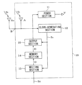
Fig. 1 is a block diagram showing an overall constitution;
Fig. 2 is a detailed block diagram;
Figs. 3A and 3B are schematic diagrams showing an overall constitution;
and
Fig. 4 is an operational diagram.
DESCRIPTION OF THE PREFERRED EMBODIMENTS
Preferred embodiments of the invention will be er;plained with reference
to the diagrams.
An IC chip for identification l0 uses a wireless system, and comprises a
power section 11, a clock-generating section 12, a writing section 13, a
memory
section 14, and an output section 15 (Fig. 1 ).
The input sides of the power section 11 and the clock-generating section
12, and the output side of the output section 15 are connected in common to an
on-chip antenna A. The on-chip antenna A is fitted with a bump B for
connecting
an outside antenna Ao. Carrier waves S 1 reach the on-chip antenna A and the
outside antenna Ao from unillustrated outside readers.
The output of the power section 11 is supplied as an internal voltage V to
the internal parts of the IC chip 10. The output of the clock-generating
section 12
CA 02480920 2004-09-09
is split to the writing section 13 and the output section 15 as an internal
clock Sc,
and the writing section 13 outputs via the memory section 14 to the output
section
15. An optical signal S2 reaches the writing section 13 from an unillustrated
outside writer.
A capacitor for resonance C is connected in parallel to the on-chip antenna
A (Fig. 2), and one end of the on-chip antenna A connects to ground.
Incidentally,
the outside antenna Ao can be appended to the on-chip antenna A via connecting
bumps B, with a capacitor for resonance C being connected in parallel to the
outside antenna Ao. However, ends of the non-grounded sides of the on-chip
antenna A and the outside antenna Ao lead separately to the power section.l 1,
the
clock generator 12, and the output section 15.
In the power section 11, ends of the non-grounded sides of the on-chip
antenna A and the outside antenna Ao are connected in common via rectifying
diodes D 1. A smoothing capacitor C 1 connects to the output side of the
diodes
D1 and Dl, and outputs the internal voltage V.
In the clock generator 12, ends of the non-grounded sides of the on-chip
antenna A and the outside antenna Ao are connected in common via detecting
diodes D2 and D2, and lead to a clock generator 12a. The input side of the
clock
generator 12a is grounded via a resistance R2, and the output of the clock
generator 12a is led as an internal clock Sc to a shift register in the
writing section
13, an overflow detector 13e, and a register lSa in the output section 15.
The writing section 13 is comprised by concatenating an amplifier 13b, a
gate circuit 13c, a shift register 13d, and the overflow detector 13e in
sequence to
a light-receiving element Ira that receives the optical signal S2 from the
outside
writer. The output of the overflow detector 13e is separately connected to a
6
CA 02480920 2004-09-09
memory 14a of the memory section 14, in addition to the gate circuit 13c. The
light-receiving element I3a comprises, for example, a photodiode.
Another output of the shift register 13d is connected to the memory 14a of
the memory section 14, and tl' a output of the memory 14a connects to the
register
1 Sa of the output section 15. The output of the register 15a is connected to
the
gate of a switching element T, such as, for example, an FET; the cathode side
of
the switching element T is grounded, and the anode side is connected via
separate
resistances RS and RS to the ends of the on-chip antenna A and the outside
antenna Ao.
The IC chip 10 may, for example, be formed as a 0.5 mm square silicon
chip (Fig. 3). Fig. 3B is a cross-sectional view taken along the arrowed line
X -
X of Fig. 3A.
The IC chip 10 is made by forming a required integrated circuit 22 on a
silicon base 21, providing an insulating layer 23 of, for example, polymide,
over
the top face of the silicon base 2I, and thereafter forming the on-chip
antenna A
and the bumps B on the insulating layer 23. The on-chip antenna A illustrated
here is a triple-wind loop antenna that is suitable for use at a frequency of
2.45
GHz, which is a representative frequency of the carrier wave Sl, and has a
metal-
plated layer formed on the insulating layer 23. Furthermore, a convex lens-
shaped light-permeable section is provided in one part of the insulating layer
23 in
order to efficiently deliver the optical signal S2 to the light-receiving
element 13a
in the integrated circuit 22.
The operation of the IC chip 10 is as follows.
When no data is written in the memory 14a of the memory section 14, the
carrier signal S 1 that carries the clock pulse is transmitted from the
outside reader
7
CA 02480920 2004-09-09
to the on-chip antenna A and/or the outside antenna Ao (topmost level of Fig.
4),
enabling the power section 11 to rectify the carrier signal S1 by using the
diodes
D1 and Dl, and create the internal voltage V (Fig. 4). The earner signal SI
has a
frequency of approximately L 0 MHz to 70 GHz, and, for example, a clock pulse
at a clock frequency fc = 1/Tc = I00 KHz (where Tc is the clock pulse cycle)
is
superimposed by 100% ASK modulation. Instead of AS)E~ modulation, the clock
pulse may be superimposed by FSK modulation, PSK modulation, or the like.
The clock generator 12a of the clock-generating section 12 can detect the
carrier
signal S 1 via the diodes D2 and D2, and create an internal clock Sc based an
the
clock pulse that is carried by the carrier signal S 1.
Next, the optical signal S2 that carries the data D is led into the light-
receiving element 13a from tile outside writer. The optical signal S2 should
preferably be an infrared beam at an auxiliary carrying frequency of S00 KHz
or
more, and the data D to be superimposed on the optical signal S2 is
synchronized
with the clock pulse carried by the carrier signal S I . The. data D is stored
in the
shift register 13d, being read serially via the gate circuit 13c into the
shift register
13d in compliance with the internal clock Sc. This is because the shift
register
13d operates in compliance with the internal clack Sc.
When a predetermined amount of data D has been stored, the shift register
13d, generates an overflow signal S~ Accordingly, the overflow detector I 3e
transmits a write signal Sw to the memory 14a of the memory section 14, writes
and stores the data D in the shift register 13d into the memory 14a, and, in
addition, transmits a gate signal Sg to the gate circuit 13c, and closes the
gate
circuit 13c, making if possible to block the passage of data D after closing
the gate
circuit I3c. That is, the memory I4a of the memory section 14 is blocked to
8
CA 02480920 2004-09-09
prevent writing thereto via the gate circuit 13c. Incidentally, the memory 14a
is a
nonvolatile memory, which holds its internal data D and stands by, even when
the
carrier signal Sl from the outside has vanished and the internal voltage V has
been lost.
When the carrier signal S I from the outside once .again reaches the on-
chip antenna A and the outside antenna Ao, the register 15a of the output
section
15 serially reads the data D in the memory I4a in compliance with the internal
clock Se, and opens or closes the switching element T in compliance with the
dat;~
D. The switching element T fluctuates the load impedance of the on-chip
antenna
A and the outside antenna Ao via the resistances R5 and R5, load-modulating
the
carrier signal S 1 in compliance with the data D (lowermost level of Fig. 4).
The
reader that transmits the earner signal S 1 is then able to read the data D in
the
memory i 4a.
In the preceding explanation, the outside antenna Ao need only he used
when necessary. When using only the on-chip antenna A, the frequency of the
carrier signal S 1 is limited to one near the resonance freduency of the on-
chip
antenna A; at this time, the reader is configured so as to sweep the frequency
of
the carrier signal S 1 and write or read data D at the optinnum frequency.
A clock pulse distinguishing function can be incorporated into the clock
generator I2a of the clock-generating section I2. An internal clock Sc is
created
only for a clock pulse at a specif c clock frequency fc, which is superimposed
on
the carrier signal Sl, thereby enabling noise tolerance to be increased. When
superimposing the clock pulse on the carrier signal S1 by ASK modulation, the
degree of modulation of the carrier signal S 1 can be set freely within a
range of
I 0% to 100%, but should preferably between set to the smallest degree of
9
CA 02480920 2004-09-09
modulation that will obtain the desired noise tolerance. This is so as to
reduce the
capacity of the smoothing capacitor C 1 of the power section 11.
The gate circuit 13c should, for example, incorporate a fuse that is blown
by the gate signal Sg, the gate circuit I3c being closed by hardware after the
fuse
has blown so as not to reopen. Since the memory 14a is securely blocked via
the
gate circuit 13c at this time, it may acceptably comprise a rewriteable flash
memory. However, the memory I4a should preferably be a non-rewriteable flash
memory, fuse memory, or the like, to ensure that the data D being stored are
not
altered.
I0
CA 02480920 2004-09-09
WHAT IS CLAIMED IS:
1. An IC chip for identification comprising:
a power section that creates an internal voltage by 'using a carrier wave
from the outside;
a clock-generating section that creates an internal clock based on a clock
pulse, which is carried on the carrier wave;
a memory section; and
an output section that serially reads data in the memory section in
compliance with the internal clock, and load-modulates the carrier wave
2. The IC chip for identiFcation as described in Claim l, further comprising
a writing section that serially reads data carried by an optical signal from
the
outside in compliance with an internal clock, and stores it in the memory
section.
3. The IC chip for identification as described in Claim 2, wherein the writing
section detects data overflow and blocks writing to the memory section
accordingly.
4. The IC chip for identification as described in Claim 3, wherein the clock-
generating section distinguishes the clock pulse that is carried by the
carrier wave.
5. The IC chip for identification as described in any one of Claims 1 to 4,
further comprising a bump for connecting an outside antenna, the bump being
fitted to an on-chip antenna that connects to the output se;etion.
11
F
' CA 02480920 2004-09-09
6. A method for reading data in an IC chip for identi~Ecation, comprising the
steps of
creating an internal clock based on a clock pulse, which is carried on a
carrier wave from the outside; and
serially reading data stored in a memory section in compliance with the
internal clock, and load-modulating the carrier wave.
7. A method for writing data in an IC chip for identification, comprising the
steps of
creating an internal clock based on a clock pulse, which is carried on a
carrier wave from the outside;
serially storing data, which is carried on an optical signal from the outside;
and
writing the stored data in a memory section, and i.n addition, blocking
writing to the memory section.
12