Note: Descriptions are shown in the official language in which they were submitted.
CA 02481380 2007-03-26
]
APPPiRATUS AND METHOD FOR MEASURING INTRAOCULAR PRESSURE
Field of the Invention
The present invention relates to an apparatus and
method for measuring intraocular pressure in an eye,=
and is particularly directed to an apparatus and method
that utilize microelectromechanical systems (MEMS)
technology to measure intraocular pressure.
CA 02481380 2004-10-08
WO 03/086168 PCT/US03/10215
-2-
Background of the Invention
The measurement of intraocular pressure (IOP) is a
routine part of an eye exam. IOP is also monitored
closely following certain surgical procedures on the
eye. IOP of an eye is typically measured using an
applanation tonometer mounted on a slit lamp bio-
microscope. Before using the applanation tonometer, an
anesthetic and a dye, such as fluorescein, are placed
in the eye.
When a cobalt blue filter is put on a light source
shined into the eye, the fluorescein dye glows a bright
green. The doctor (or technician) then looks through
the tonometer and turns a dial until the tonometer tip
flattens a given amount of the corneal surface of the
eye. The amount of IOP is calculated using the
relationship between (i) the force required to flatten
the cornea (in mmHg) and (2) the area of cornea
flattened. During this process, the tonometer tip,
,which is usually a plastic part or a glass prism.that
has been disinfected with an alcohol wipe, touches the
front of the cornea. It is desirable to provide an
apparatus for measuring IOP in which the tip of the
tonometer includes a disposable, and thus extremely
sanitary, pressure sensor.
CA 02481380 2008-03-10
- 3 --
Summary of the Invention
The present invention is an apparatus for
measuring intraocular pressure of an eye. The
apparatus comprises an applanation tonometer having a
distal end that is movable toward the eye and a
disposable module positioned at the distal end of the
applanation tonometer. The module includes a sensor
carrier and a sensor connected to the sensor carrier.
The sensor comprises a contact surface for making
contact with a surface portion of the eye. The contact
surface includes an outer non-compliant region and an
inner compliant region fabricated as an impedance
element that varies in impedance as the inner compliant
region changes shape. The sensor further comprises a
region of conductive material that is electrically
coupled to the impedance element of the compliant
region and responsive to an external signal for
energizing the impedance element so that the
intraocular pressure may be determined. An antenna is
positioned at the distal end of the applanation
tonometer for transmitting the external signal for
energizing the impedance element.
The present invention also provides a method for
measuring intraocular pressure (lOP) of an eye.
According to the inventive method, an applanation
tonometer is provided with a distal end that is movable
toward the eye. A disposable module is positioned at
CA 02481380 2008-03-10
-4-
the distal end of the applanation tonometer. The module
includes a sensor carrier and a sensor connected to the
carrier. The sensor has a compliant region that
functions as an impedance element. The distal end of
the applanation tonometer is moved until the sensor
comes into contact with a surface portion of the eye
which causes the compliant region to change shape and
vary in impedance. An activation signal is transmitted
over the antenna to energize an inductive region of the
sensor that is connected to the impedance element which
is a capacitive region to cause a circuit formed by the
regions to resonate. A representative pressure
measurement is determined each time the impedance
element is energized. The representative pressure
measurements are processed to render a resultant IOP
measurement.
Brief Description of the Drawings
The foregoing and other features of the present
invention will become apparent to those skilled in the
art to which the present invention relates upon reading
the following description with reference to the
accompanying drawings, in which:
Fig. 1 is a cross-sectional view of a first
embodiment of a tonometer sensor for use in the present
invention;
Fig. 2 is a plan view of the tonometer sensor of
Fig. 1;
CA 02481380 2004-10-08
WO 03/086168 PCT/US03/10215
-5-
Figs. 3A and 3B are cross-sectional and plan
views, respectively, of the tonometer sensor
illustrating additional regions in accordance with the
present invention;
Figs. 4A and 4B are cross-sectional and plan
views, respectively, of a tonometer sensor constructed
in accordance with an alternate embodiment of the
present invention;
Fig. 5A is a graph illustrating the relationship
between deflection of the tonometer sensor and
intraocular pressure (IOP);
Fig. 5B is a graph illustrating the relationship
between resonant frequency of the tonometer sensor
and I P;
Figs. 6(al)-6(i2) are cross-sectional and plan
views, respectively, of the tonometer sensor through
various stages of a fabrication process;
Figs. 7(al)-7(j2) are cross-sectional and plan
views, respectively, of an alternate tonometer sensor
through various stages of a fabrication process;
Figs. 8(al)-8(d) are cross-sectional and plan
views of another alternate tonometer sensor through
various stages of a fabrication process;
CA 02481380 2004-10-08
WO 03/086168 PCT/US03/10215
-6-
Fig. 9 is an illustration of an apparatus for
measuring IOP of an eye using the tonometer sensor of
Fig. 3;
Fig. 10A is an illustration of the tonometer
sensor mounted in a disposable carrier and attached to
an end of the apparatus of Fig. 9;
Fig. 10B is a sectional view taken along
line 10B-10B in Fig. 1OA;
Figs. 11A1-11E2 are illustrations of the response
of the apparatus of Fig. 9 to contact with an eye;
Fig. 12 is a functional block diagram schematic of
a control unit for use with the apparatus of Fig. 9;
Fig. 13 is an illustration of the tonometer sensor
mounted in a carrier constructed in accordance with an
alternate construction of the first embodiment;
Fig. 14 is a sectional view taken along line 14-14
in Fig. 13;
Fig. 15 is a sectional view of a tonometer sensor
constructed in accordance with a second embodiment of
the present invention, the sensor being shown
responding to a magnetic field;
Fig. 16A is a time graph illustrating a magnetic
field strength vs. time envelope for the tonometer
sensor of Fig. 15;
CA 02481380 2004-10-08
WO 03/086168 PCT/US03/10215
-7-
Fig. 16B is a graph illustrating the frequency
sweep of an activation signal over a time interval for
the tonometer sensor of Fig. 15;
Fig. 17 is a schematic illustration of the
tonometer sensor mounted in a carrier constructed in
accordance with the sensor embodiment;
Fig. 18 is a sectional view taken along line 18-18
in Fig. 17;
Fig. 19 is a sectional view illustrating a
configuration for a portion of Fig. 17; and
Fig. 20 is a functional block diagram schematic of
a control unit for use with the apparatus of Fig. 17.
Detailed Description of Embodiments
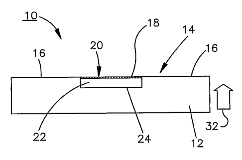
A tonometer sensor 10 produced using
microelectromechanical system (MEMS) techniques is
shown in Figs. 1 and 2. The tonometer sensor 10
includes a substrate 12 that is comprised of a silicon
material, but it should be understood that other
materials may be used. The substrate 12 includes a
contact surface 14 for making contact with a surface
portion 34 (Fig. 3A) of an eye 36. The surface 14
includes an outer non-compliant region 16 (Fig. 1) and
an inner compliant region 18 that is fabricated using
MEMS techniques (which will be described in greater
CA 02481380 2004-10-08
WO 03/086168 PCT/US03/10215
-8-
detail herein below) as an impedance element, the
impedance of which varies as the inner compliant
region 18 changes shape. The compliant region 18
comprises a diaphragm 20 as one plate of a capacitive
element that is separated by a dielectric 22 from
another plate 24 of the capacitive element which is
part of the non-compliant region 16. As will become
more evident from the description below, as the contact
surface 14 is pressed against the surface portion of
the eye, the diaphragm plate 20 flexes closer to the
other non-compliant plate 24 to change the capacitance
of the capacitive element in proportion to the
intraocular pressure (IOP) of the eye. In the
illustrated embodiment, the dielectric comprises air,
but other suitably compliant dielectrics such as
hydrogel and silicone, for example, may also be used,
without deviating from the principles of the present
invention.
As shown by the substrate cross-sectional and plan
views of Figs. 3A and 3B, respectively, a region of
conductive material 38 is included as part of the
substrate 12 and is electrically coupled to the
impedance element of the compliant region 18
(diaphragm 20) which is a capacitive element. While
CA 02481380 2004-10-08
WO 03/086168 PCT/US03/10215
-9-
not shown in Figs. 3A and 3B, this electrical coupling
is described in greater detail in connection with the
fabrication drawings found herein below. The
conductive material 38 is responsive to an external
signal for energizing the impedance element so that
the IOP may be determined. In Figs. 3A and 3B, the
conductive region 38 comprises an inductor coil
fabricated in the non-compliant region 16 of the
contact surface 14 such that it is electrically coupled
to the capacitive element to form a resonance or tank
circuit. It should be understood that other types of
sensors (piezoelectric, piezoresistive, strain-gage
based, etc.) could be substituted for the sensor 10.
Such other types of sensors would likely require use of
other known telemetry techniques rather than a tank
circuit.
In the present embodiment, the inductor coil 38 is
formed by disposing conductive material in a
predetermined pattern, like a concentric spiraled
pattern, for example, in the non-compliant region 16.
A process for fabricating the inductor coil 38 at the
non-compliant region 16 is described in greater detail
herein below. However, it should be understood that
the inductor region need not be embodied solely at the
CA 02481380 2004-10-08
WO 03/086168 PCT/US03/10215
-10-
non-compliant region 16 and may be embodied as part of
the compliant region 18 as well without deviating from
the principles of the present invention. Further, it
should be understood by those of ordinary skill in the
art that there could be a spiral inductor 42 on the
contact surface 14 of the diaphragm 20 coupled to a
flat spiral inductor 44 underneath the diaphragm as
illustrated in the alternate embodiment of Figs. 4A
and 4B. Yet another alternative would include a
combination of the aforementioned spiral inductor 42
and the capacitive element, formed by the diaphragm
(plate) 20 and the fixed plate 24, acting in
conjunction with each other, meaning the inductance and
the capacitance will increase (as the plates get closer
to each other) or decrease together.
In the present embodiment, the resonant circuit
comprising the inductor coil 38 and the capacitive
element formed by the plates 20 and 24 may be excited
into resonance by an external electromagnetic signal in
the radio frequency (RF) range. Tank circuits of this
type have a natural resonant frequency fo that, to the
first order, depends of the values of the inductor and
the capacitor as follows:
fo = 1/2n (LC) 1/2
CA 02481380 2004-10-08
WO 03/086168 PCT/US03/10215
-11-
where L is the inductance and C is the capacitance.
Accordingly, as the capacitance of the tonometer
sensor 10 changes, the resonant frequency .fo of the
tank circuit will change in proportion thereto.
For example, if the contact area 14 of the
tonometer sensor 10 is approximately one square
millimeter (1 mm2) or one millimeter (1 mm) on each
side, the diaphragm 20 of the compliant region 18 may
have a diameter of five hundred micrometers (500 pm)
with a one and a half micrometer (1.5 pm) dielectric
or air gap, and the inductor coil may have
twenty-five (25) turns with an inside diameter (ID)
of five hundred micrometers (500 pm) and an outside
diameter (OD) of one thousand micrometers (1,000 }zm).
With the diaphragm 20 undisturbed, the resonant
frequency may be on the order of one hundred and
ninety-three megahertz (193 MHz). Accordingly, a ten
percent (10%) increase in capacitance, for example,
resulting from a diaphragm 20 deflection will produce a
downward shift in resonant frequency to one hundred and
eighty-four point one megahertz (184.1 MHz) and this
shift in resonant frequency is readily discernible
electronically as will be further described herein
below. It is understood that the contact area of the
CA 02481380 2004-10-08
WO 03/086168 PCT/US03/10215
-12-
sensor 10 may be less than 1 mm, in which case the
various dimensions may be rescaled proportionately.
As has been described in connection with the
illustration of Fig. 3A, the deflection of the
diaphragm 20 of the compliant region 18 as the contact
surface 14 of the substrate 12 is pressed against the
surface portion 34 of the eye 36 is representative of
the IOP of the eye. The graph of Fig. 5A illustrates
an exemplary center deflection in micrometers (pm)
expected for a diaphragm 20 with the geometry described
above as a function of the IOP of the eye expressed in
parametric units of millimeters of Mercury (mm Hg). It
is this deflection of the diaphragm 20 which causes the
change in capacitance and may be measured by the
resultant change in resonant frequency of the tank
circuit. The graph of Fig. 5B illustrates an estimated
change in resonant frequency based upon a conservative
approximation of a corresponding change in capacitance
resulting from the deflection of the diaphragm 20 due
to IOP. The expression of resonant frequency (MHz)
to IOP (mm Hg) illustrated by the graph is nonlinear as
expected in a capacitive sensing structure for
measuring IOP.
CA 02481380 2004-10-08
WO 03/086168 PCT/US03/10215
-13-
An exemplary process suitable for fabricating an
embodiment of the tonometer sensor 10 is shown in the
process diagrams of Figs. 6(al) through 6(i2) wherein
each Figure provides cross-sectional and plan views,
respectively, of the sensor structure at various stages
of the fabrication process. The process starts with a
substrate 100 which may be part of a silicon wafer, for
example, as shown in Fig. 6(a). It is understood that
materials other than silicon may be used for the
substrate in which case the process may be slightly
modified to accommodate such other material. The
substrate has a top surface 102 and a bottom
surface 104. In the step of Fig. 6(b), an etch
resistant layer is provided over the substrate, like
silicon dioxide (Si02), for example, and the top
surface 102 is patterned using conventional
lithograph/etching processes to form the capacitor well
region 106 having a diameter of approximately 500 pm,
for example, and spiraled groove regions 108 of a width
on the order of 5 pm, for example, for the inductor
coil. Thereafter, the unpatterned etch resist areas of
the Si substrate are etched using a deep etch process,
like reactive ion etching, for example, to a depth of
CA 02481380 2004-10-08
WO 03/086168 PCT/US03/10215
-14-
one to twenty microns and the etch resist is removed
rendering a structure as shown in Fig. 6(b).
In the step of Fig. 6(c), a layer of silicon
nitride (Si3N4) or other similar material 110 is
deposited on the surfaces of the substrate 100. A
conformal coating of Si3N4 is deposited over the surface
of the substrate through a conventional chemical vapor
deposition (CVD) process to a thickness of
approximately 1200 A - 2400 A, for example. Next, in
the step of Fig. 6(d), a layer of low temperature
oxide (LTO) 112 is deposited over the Si3N4 layer 110
by conventional CVD to a thickness of approximately
2-3 pm, for example. The LTO layer 112 of the top
surface 102 is polished smooth using a chemical
mechanical polishing process, for example, and
patterned using a conventional photolithography process
to form an anchor region 114 which, for the present
embodiment, is in the form of an annulus of a width of
approximately 50-100 microns surrounding the capacitive
well region 106. The anchor region 114 is etched
through the LTO layer 112 down to the Si3N4 layer 110
using a reactive ion etching process, or a wet etching
process using buffered hydrofluoric acid (BHF), or
other similar process.
CA 02481380 2004-10-08
WO 03/086168 PCT/US03/10215
-15-
In the step of Fig. 6(e), a layer of
polysilicon 118 is deposited, preferably by CVD,
over the surface of the LTO layer 112 of Fig. 6(d) and
the layer of polysilicon at the top surface 102 is
patterned and etched in a conventional manner to form
an unetched layer of polysilicon 120 covering
substantially the capacitive well region 106 and
anchored by region 114 to the nitride layer. A
hole 122 may be provided through an edge of the
polysilicon layer 120 to the LTO and Si3N4 layers 112
and 110 thereunder by the aforementioned patterning and
etching process of Fig. 6(e). A post annealing process
is performed to render the membrane section of
polysilicon 120 in tension. In the present embodiment,
the structure of Fig. 6(f) is put in an oven and heated
for approximately 30 minutes at approximately 900 C
which changes the crystalline makeup of the polysilicon
to provide for stress modification thereof.
In the step of Fig. 6(f), the LTO and nitride
layers 112 and 110, including the layers under the
polysilicon layer 120, are removed, preferably by a
conventional BHF etching process wherein the BHF is
allowed to flow through the hole 122 and etch the LTO
and nitride layers under the polysilicon layer 120
CA 02481380 2004-10-08
WO 03/086168 PCT/US03/10215
-16-
which are released in solution through the same
hole 122. Accordingly, a polysilicon diaphragm 120 in
tension is produced as shown in Fig. 6(f). Next, the
hole 122 in the polysilicon diaphragm is sealed by
growing a low temperature oxide layer (not shown) over
the hole 122 in a conventional furnace environment.
In the step of Fig. 6(g), the grooved areas 108
may be pretreated to accept a conductive material which
may be deposited in the grooves by conventional
plating, sputtering or evaporation techniques, for
example, to form the inductor coil 124. Metals which
may be used for this process include Ni, Au, Fe, Ag,
and Pt to name a few. Preferably, the metallic plating
is performed electroless, but electroplating may also
be used without deviating from the principles of the
present invention.
As shown in Fig. 6(h), interconnects 126 and 128
are provided from the ends of the inductor coil 124 to
corresponding sides of the capacitive element. For the
interconnect region 126, a window is formed in the
nitride layer 110 between the conductive material of
the inside coil 130 and the polysilicon layer 120 which
is one side of the capacitive element of the sensor 10.
When the window region is plated, the metal end 130 of
CA 02481380 2004-10-08
WO 03/086168 PCT/US03/10215
-17-
the inductor coil 124 will make electrical contact with
one side 120 of the capacitive element. For the
interconnection region 128, a window is formed in the
nitride layer 110 between the substrate and the groove
of the other end 132 of the coil 124 such that when
plated, metal electrically connects the other end 132
of the coil 124 with the silicon substrate 100, which
is the other side of the capacitive element, thus,
completing the tank or oscillatory circuit. In the
step of Fig. 6(i), a thin layer of non-conducting
material 136 may be grown over the metallic plated
surfaces of the non-compliant region 16 to ensure
against the sections of the inductor coil 124 making
contact with each other over the surface of the nitride
layer 110.
An embodiment for illustrating a fabrication
process of an alternate embodiment of the tonometer
sensor 10 is shown in the Figs. 7(al) through 7(j2)
wherein each Figure provides cross-sectional and plan
views, respectively, of the alternate sensor structure
at various stages of the fabrication process. The
process starts with a substrate 140 which may be part
of a silicon wafer, for example, as shown in Fig. 7(a).
It is understood that materials other than silicon may
CA 02481380 2004-10-08
WO 03/086168 PCT/US03/10215
-18-
be used for the substrate in which case the process may
be slightly modified to accommodate such other
material. The substrate 140 has a top surface 142 and
a bottom surface 144. In the step of Fig. 7(b), a
layer of silicon nitride (Si3N4) or other similar
material 146 is deposited on the top and bottom
surfaces 142 and 144 of the substrate 140. In the
present embodiment, the Si3N4 146 is deposited through a
conventional chemical vapor deposition (CVD) process to
a thickness of approximately 1200 A, for example.
Next, in the step of Fig. 7(c), a layer of low
temperature oxide (LTO) 148 is deposited over the Si3N4
layer 146 by conventional CVD to a thickness of
approximately 1.5 pm, for example. The LTO layer 148
of the top surface 142 is patterned using a
conventional photolithography process to form a circled
region 150 having a diameter of approximately 500 pm,
for example, on top of the Si3N4 layer 146, and the
unpatterned regions 152 around the circled region 150
and on the bottom surface 144 are etched using a
reactive ion etching process or a wet etching process
using buffered hydrofluoric acid (BHF), or other
similar process.
CA 02481380 2004-10-08
WO 03/086168 PCT/US03/10215
-19-
The top surface 142 of the resulting structure as
shown in Fig. 7(d) is deposited with another low
temperature oxide layer, preferably by CVD, to a
thickness of approximately 0.5 pm, for example. This
second LTO layer 154 is patterned and etched in a
conventional manner such that the remaining unetched
second LTO layer overlaps the circled layer 150
concentrically to form an annular region of
approximately 50 pm on top of the Si3N4 layer 146
surrounding the circled region 150 as shown in
Fig. 7 (e) .
In the step of Fig. 7(f), a layer of polysilicon
is deposited, preferably by CVD, over the top
surface 142 of the structure of Fig. 7(e), and the
layer of polysilicon is patterned and etched in a
conventional manner to form an unetched layer of
polysilicon 156 covering substantially the second LTO
layer 154. A hole 158 may be provided through the
polysilicon layer 156 to the LTO layers 150, 154
thereunder by the aforementioned patterning and etching
process of Fig. 7(f). A post annealing process is
performed to render the membrane section of
polysilicon 156 in tension. In the present embodiment,
the structure of Fig. 7(f) is put in an oven and heated
CA 02481380 2004-10-08
WO 03/086168 PCT/US03/10215
-20-
for approximately 30 minutes at approximately 900 C
which changes the crystalline makeup of the polysilicon
to provide for stress modification thereof.
In the step of Fig. 7(g), the LTO layers 150
and 154 under the polysilicon layer 156 are' removed by
a conventional BHF etching process wherein the BHF is
allowed to flow through the hole 158 and etch the LTO
layers under the polysilicon layer 156 which are
released in solution through the same hole 158.
Accordingly, a polysilicon diaphragm 156 in tension is
produced. Next, the hole 158 in the polysilicon
diaphragm is sealed by growing a low temperature oxide
layer over the hole in a conventional furnace
environment.
Next, in the step of Fig. 7(h), a polymer
layer 160 which may be a photosensitive polyimide, a
photoresist material, PMMA, or the like, is deposited
over the Si3N41ayer 146 of the top surface 142.
Patterning of the polymer layer depends on the type of
polymer used. For example, if a polyimide is used,
conventional photolithography may be used to form the
annular winding pattern of the inductor coil 124. The
patterned portions of the polyimide are etched
conventionally down to the Si3N4 layer 146 to provide
CA 02481380 2004-10-08
WO 03/086168 PCT/US03/10215
-21-
grooves 162 in which to plate the metallic material of
the inductor coil 124 within the polyimide layer 160 on
the Si3N4 layer 146 as shown in Fig. 7(i). Preferably,
the metallic plating is performed electroless, but
electroplating may also be used without deviating from
the principles of the present invention. One
groove 164 in the polyimide layer 160 goes down to the
annulus of the polysilicon layer 156 so that when
plated, the metal end of the inductor coil 124 will
make contact with the polysilicon 156 which is one side
of the capacitive element of the sensor 10. In
addition, a hole may be provided through the Si3N4
layer 146 at the groove 166 of the other end of the
inductor coil 124 to allow the plated metal in the
groove 166 to pass through the hole and make contact
with the silicon substrate 140, which is the other side
of the capacitive element, thus completing the tank or
oscillatory circuit. As shown in Fig. 7(j), a thin
layer of non-conducting material may be grown over the
metallic plated surfaces 172 of a non-compliant region
to ensure against the sections of coil making contact
with each other over the surface of the polyimide
layer 160.
CA 02481380 2004-10-08
WO 03/086168 PCT/US03/10215
-22-
While the present MEMS sensor 51 is described as
being fabricated on a silicon substrate, it is
understood that other substrates may be used such as a
polymeric material, including plastics and polymer
films, for example. Such an alternate MEMS sensor 51
could be fabricated using a well-known
micro-replication process such as is illustrated in
Figs. 8(a)-8(d), with the simultaneous fabrication of
two of the sensors 51 being shown side by side. In
Figs. 8(al) and 8(a2), a thin film of plastic or
polymer is mechanically patterned, preferably with
dimples that would represent wells 54, by a
conventional process. The film 52 would then be
metalized to form a ground electrode 56. A second
film 58 (Fig. 8(bl) could be metalized in a pattern to
form an inductor 60 and capacitor (tank circuit). The
two films 52 and 58 are then aligned and ultrasonically
bonded together. Following a final metallization step
(Fig. 8(d)) in which a metal is passed through a
hole 59 in the second film 58 to form interconnecting
conductors 61, the tonometer sensor 51 has a structure
similar to the structures described herein above for a
silicon substrate, but made from a plastic or polymer
film instead.
CA 02481380 2004-10-08
WO 03/086168 PCT/US03/10215
-23-
Referring now to Fig. 9, an apparatus 176 that
uses the sensor 10 to measure IOP is illustrated. The
apparatus 176 comprises a known slit lamp
biomicroscope 178 with an applanation tonometer
mechanism 180. On the slit lamp biomicroscope 178, the
applanation tonometer mechanism 180 includes one or
more movable arms 182 that are adjustable by dials (not
shown) and/or levers (not shown), as is known in the
art, to move the sensor 10 which is mounted, as
described below, at the distal end of the mechanism
into contact with an eye for IOP measurement. It
should be understood that one or more stepper motors
could also be used in the applanation tonometer
mechanism 180 to adjust and advance the position of the
applanation tonometer mechanism.
At its distal end, the applanation tonometer
mechanism 180 includes a holder 184 (Figs. 10A and lOB)
to which the sensor 10 is attached. The holder 184
includes a slot 186 for receiving a sensor module 188
and an antenna 190 (shown schematically in Fig. 10A)
for transmitting to and receiving electrical signals
from the tank circuit on the sensor 10. The sensor
module 188 comprises the sensor 10 which is attached to
a dielectric sensor carrier 192 by a dielectric
CA 02481380 2004-10-08
WO 03/086168 PCT/US03/10215
-24-
adhesive 194, such as an epoxy. The sensor carrier 192
includes a pair of oppositely disposed flanges 196 that
snap-fit into the slot 186 in the holder 184, although
it should understood that the attachment between the
sensor carrier 192 and the holder 184 could have many
different configurations.
As the contact surface of the tonometer sensor 10
is pressed against the surface portion of the eye, the
response of the tonometer sensor 10 over time is shown
in the illustrations of Figs. 11A1 through 11E2. Each
of the Figs. 11A through 11E provide an illustration of
the position of the sensor'10 in relation to the eye 36
and a corresponding time graph of a pressure
representative signal vs. time. The darkened region
along each time graph is the time interval represented
by the respective illustration. In Fig. 11A, advancing
the sensor 10 toward the cornea surface of the eye 36
causes the sensor to flex. In Fig. 11B, the compliant
region 18 of the sensor 10 initially meets the surface
of the eye 36. The initial dip in pressure at 60 from
the base line pressure 62 may be due to surface tension
attracting the diaphragm of the compliant region 18
just before actual contact with the eye surface.
CA 02481380 2004-10-08
WO 03/086168 PCT/US03/10215
-25-
Accordingly, as the sensor 10 is pressed further
against the eye surface and the diaphragm is depressed
as shown in Fig. 11C, the pressure representative
signal will continue to increase. As the flattening of
the eye surface increases, the sensed pressure peaks,
as shown at point 64 in Fig. 11D, starts to decrease as
a result of the bending forces of the cornea being
transferred from the compliant region 18 to across the
non-compliant region 16 of the sensor 10. Point 64
represents the initial crest of the pressure ,
representative signal. As the sensor 10 is pressed
further against the eye surface as shown in Fig. 11E,
the pressure reaches a minimum at point 66 and this
minimum represents the IOP of the eye 36. Thereafter,
as the sensor 10 is moved farther toward and against
the eye surface, the pressure increases beyond the IOP
stage due primarily to an artificial elevation of IOP
resulting from additional applanation and other forces
in the eye, such as, surface tension from tearing shown
at 68, bending force shown at 70, and tissue tension
shown at 72, for example. After the IOP has been
measured via the sensor 10, the sensor is returned back
to its original starting position and the pressure
CA 02481380 2004-10-08
WO 03/086168 PCT/US03/10215
-26-
reading is baselined at level 62. The sensor 10 is
then ready for the next IOP measurement.
In order to take the IOP measurements from the
sensor 10, a control unit 50 (Figs. 9 and 10B) is
provided and is operatively coupled, in a manner not
shown, to the antenna 190 in the holder 184. The
control unit 50 generates the activation signal for
energizing the impedance element of the sensor 10 to
measure a signal representative of the IOP. This
activation signal is preferably an electromagnetic
signal that varies over a predetermined radio frequency
range say from one hundred to two hundred
megahertz (100-200 MHz), for example, that energizes
the tank circuit of the sensor 10 and causes it to
resonate. The control unit 50 may also include a
circuit to detect the resonant frequency of the
sensor's tank circuit which is proportional to the IOP
as shown by the graph of Fig. 5B, for example. This
activation signal may be transmitted from the control
unit 50 multiple times over a predetermined time
interval during which the sensor 10 is in contact with
the eye 36. Each electromagnetic activation signal is
ramped from a starting frequency flto an ending
frequency f2 in order for a resonant frequency to be
CA 02481380 2004-10-08
WO 03/086168 PCT/US03/10215
-27-
determined which is representative of a pressure
measurement sampling point during the application of
the sensor 10 to the eye 36. The collection of this
pressure measurement data (or sampling points) provides
for a pressure vs. time graph, as exemplified by
Fig. 11E, in order to determine the minimum or
actual IOP.
A schematic block diagram of the control unit 50
for use in of the present invention is shown in
Fig. 12. Referring to Fig. 12, a circuit 200 may be
triggered by a signal 202 to generate a linear ramping
signal 204 which ranges from voltages V1 to V2 over a
predetermined time interval At, on the order
of 1 millisecond, for example. At the end of the
time interval At, the voltage returns to a
predetermined voltage setting to wait for the next
trigger signal over line 202. The linear ramping
signal 204 governs a voltage controlled oscillator
(VCO) circuit 206 to generate a sinusoidal signal 208
which overlaps the frequency range of the sensor 10 as
the signal 204 ramps from V1 to V2. The signal 208 may
be amplified by a radio frequency (RF) amplifier
circuit 210 which drives a resistor/inductor series
combination, R1 and L1, respectively. The output of
CA 02481380 2004-10-08
WO 03/086168 PCT/US03/10215
-28-
the RF amplifier 210 may be provided to a pulse shaper
circuit 212 over signal line 214 which in turn is
coupled to a cascaded pair of digital counters 216
and 218. The digital output of counter 218 is captured
in an output buffer 220.
The voltage across the inductor L1 is input to
another RF amplifier 222 via signal line 224. The
output 226 of the RF amplifier 222 is provided to a
root-mean-square (RMS) detector 228, the output 230 of
which being coupled to a comparator circuit 232. In
the present embodiment, the comparator circuit 232
functions as a signal peak or valley detector and
generates a signal over line 234 when the signal peak
or valley is detected. The signal line 234 is coupled
to the counter 218 and output buffer 220 for operation
thereof. The circuits of the control unit 50 may be
centrally controlled in operation by a digital
controller 240, which may be a programmed
microprocessor, digital signal processor or a
combination of hardwired digital logic circuits. A
memory unit 242 is coupled to the digital
controller 240 and may be comprised of a combination
of static, dynamic and read-only memory units, for
example, for the storage of data and program
CA 02481380 2004-10-08
WO 03/086168 PCT/US03/10215
-29-
information. A switch 244 which may be of the push
button variety, for example, is coupled to the digital
controller 240 through conventional input-output
circuitry (not shown). The digital controller 240 may
also be coupled to a conventional display unit 246 for
displaying IOP readings. The control unit 50 may also
include an upload/download circuit 250 for transmitting
data between the digital controller 240 and an external
computer, like a PC, for example, over a hardwired
connection.
Taking an IOP reading'using the control unit 50 in
combination with the sensor 10 will now be described in
connection with Figs. 9, 10A, 10B, 11E, and 12. A
coarse alignment of the sensor 10 with the eye 36, as
illustrated in Fig. 9, is done by the doctor or
technician looking through the slit lamp
biomicroscope 176. The dials/levers of the
applanation tonometer mechanism 180 are then adjusted
by the operator until the sensor 10 is moved to the
position of Fig. 11A1. Once the sensor 10 is brought
in close proximity to the eye 36 as shown in Fig. 11A1,
the switch 244 may be depressed for taking an IOP
reading. In response to the depression of the
switch 244, the digital controller 240 commences with a
CA 02481380 2004-10-08
WO 03/086168 PCT/US03/10215
-30-
sequence of control operations to perform the IOP
reading.
Following pushing of the switch 244, trigger
signals are generated at predetermined times over
signal line 202 to cause the linear ramp circuit 200 to
generate the ramping signals which controls the VCO
circuit 206 to drive the inductor L1 via RF amplifier
circuit 210 and resistor R1. In turn, the inductor L1
is coupled magnetically to the inductor of the
sensor 10 and electromagnetically activates and drives
the tank circuit of the sensor. As has been described
herein above, the capacitive element (compliant
region 18) of the sensor 10 will change in impedance as
it is forced against the surface portion 34 of the
eye 36. This change in impedance will cause a change
in circuit resonance. Sensor readings are thus taken
at the points of resonance of the magnetically coupled
circuits. More specifically, during the time interval
of each frequency ramp, the RMS voltage across the
inductor L1 is monitored by the circuits 222, 228,
and 232 to establish the point in time of resonance.
At resonance, a signal is generated by the comparator
circuit 232 to the digital controller 240, the
counter 218, and the output buffer 220. In response to
CA 02481380 2004-10-08
WO 03/086168 PCT/US03/10215
-31-
this signal, the digital count of the counter 218 which
is representative of the resonance frequency is
captured in the output buffer 220 and subsequently,
read by the controller 240 and stored in the
memory 242. When the digital count has been read and
stored, the control unit 50 generates an audible signal
to indicate to the operator that it is time to move the
sensor 10 to the subsequent position as shown in
Figs. 11A-11E. The stored digital counts of each of
the frequency sweep time intervals represent sampled
data points which together form the pressure profile of
Fig. 11E. The digital controller 240 processes these
sampled data points to determine the current IOP
reading which may be day and time stamped and stored in
the memory 242 and displayed in the digital
display 246.
Figs. 13 and 14 illustrate an alternate
construction for the first embodiment of the present
invention in which the antenna 190 is integrated into
the disposable sensor carrier 192. When the sensor
carrier 192 is inserted into the slot 186 in the
holder 184, electrical connection between the
antenna 190 and the control unit 50 is made by
contacts 198 at one end of the carrier engaging
CA 02481380 2004-10-08
WO 03/086168 PCT/US03/10215
-32-
contacts on the holder. In all other aspects, the
structure and function of the alternate construction
illustrated in Figs. 13 and 14 is the same as
previously described.
Figs. 15-20 illustrate a tonometer sensor 10'
constructed in accordance with a second embodiment of
the present invention. In Figs. 15-20, reference
numbers that are the same as those used in Figs. 1-14
designate components and features that are the same.
As may be seen in Fig. 15, the substrate 12 of the
tonometer sensor 10' includes a region of material 26
that is responsive to a non-invasive external force to
press the contact surface 14 against the surface
portion 34 of the eye 36 and thereby cause the
compliant region 18 (diaphragm 20) to change shape in
proportion to the IOP of the eye (refer again to
Fig. 3A). The region of material 26 comprises a magnet
responsive to a magnetic field 30 as shown in Fig. 15.
The surface 28 of the substrate 12 is layered with a
magnetic material that forms a permanent magnet 29 with
its North-South poles aligned along an axis transverse
to the contact surface 14. The magnetic material may
be plated or bonded to the surface 28 and may include
plated Permalloy, plated iron, plated CoNiMnP, a screen
CA 02481380 2004-10-08
WO 03/086168 PCT/US03/10215
-33-
printed polymer composite, and rolled magnetic films.
In use, as a magnetic field is brought in proximity to
the permanent magnet 29, the substrate 12 is repulsed
by the magnetic field with a force 32. The strength of
the magnetic field determines the force 32 at which the
contact surface 14 is pressed against the surface
portion 34 of the eye 36. It should be understood that
the magnet 29 could also be plated to the sensor 51 of
Figs. 8(al)-8(d) so that the micro-replicated sensor 51
could be substituted in the embodiment of Figs. 15-20.
Referring now to Fig. 17, a sensor module 188',
which includes the tonometer sensor 10', is used with
the slit lamp biomicroscope 178 (Fig. 9) and the
applanation tonometer mechanism 180 to measure IOP.
The tonometer sensor 10' of Fig. 17 is connected to the
sensor carrier 192 by spring means 280. In one
embodiment illustrated in Figs. 18 and 19, the spring
means 280 comprises a plurality of spring arms 282 that
are attached, by epoxy or other suitable means, to both
the tonometer sensor 10' and the carrier 192. The
spring arms 282 allow relative axial movement of the
tonometer sensor 10' in response to an electromagnetic
activation signal as discussed further below.
CA 02481380 2004-10-08
WO 03/086168 PCT/US03/10215
-34-
In order to activate the magnet 29, a control
unit 50' (Fig. 20) includes a magnetic field generation
unit 260 which is a conventional coil circuit for
generating a magnetic field 261 electromagnetically.
The magnetic field generation unit 260 may be
constructed integrally with the antenna 190 and located
at the distal end of the applanation tonometer
mechanism 180. A magnetic field control circuit 262 is
included to control the magnetic field strength
according to the time curve shown in Fig. 16A by
adjusting a current signal 264 applied to the field
generation unit 260. A feedback signal 266 may be
supplied from the field generation unit 260 to the
control unit 262 to provide for a more accurate
magnetic field strength vs. time profile generation.
An initiation signal is provided from the digital
controller 240 to the field control unit 262 over a
signal line 268. Alternatively, the activation signal
from the RF amplifier 210 may be capacitively coupled
to the field control circuit 262 for superimposing the
activation signal on the magnetic field signal as shown
in the profile of Fig. 16A. A further alternative
would be to control the magnetic field strength through
CA 02481380 2004-10-08
WO 03/086168 PCT/US03/10215
-35-
the RF amplifier by varying the DC bias thereto in
accordance with the profile of Fig. 16A.
In use, following rough alignment of the
applanation tonometer mechanism 180, with the sensor
module 188' attached thereto, to the eye 36, the
control unit 50' generates the magnetic field 30 over a
predetermined time interval to create the repulsive
force 32 that presses the contact surface 14 against
the eye 36. The strength of the magnetic field 30 may
be varied by the control unit 50' over the
predetermined time interval to cause the contact
surface of the sensor 10' to be pressed against, and
subsequently released from, the surface portion of the
eye with a respective varying force. The graph of Fig.
16A illustrates the magnetic field strength envelope
over a time interval of one to two seconds.
The electromagnetic activation signal may be
superimposed on the magnetic field signal illustrated
in Fig. 16A. For each interval At which is much
smaller than the predetermined time interval over which
the magnetic field is being applied, the
electromagnetic signal is ramped from a starting
frequency f1 to an ending frequency f2 as illustrated in
Fig. 16B. The range of all possible frequencies
CA 02481380 2004-10-08
WO 03/086168 PCT/US03/10215
-36-
representative of measured IOP's during the application
of the magnetic field will fall within the frequency
range of Fig. 16B. Accordingly, for each interval At,
a resonant frequency is determined which is
representative of a pressure measurement sampling point
during the application of the magnetic field and the
collection of these pressure measurement sampling
points provides for a pressure vs. time graph, as
exemplified in Fig. 11E, in order to determine the
minimum or actual IOP.
From the above description of the invention, those
skilled in the art will perceive improvements, changes
and modifications. Such improvements, changes and
modifications within the skill of the art are intended
to be covered by the appended claims.