Note: Descriptions are shown in the official language in which they were submitted.
CA 02481923 2007-11-16
METHOD OF BALANCING DISPLAY PANEL COLOUR USE
USING A SCREEN SAVER
FIELD OF THE INVENTION
The present invention relates generally to mobile electronic devices. More
particularly, the present invention relates to a method and system for
providing a screen
saver in a mobile electronic device.
BACKGROUND OF THE INVENTION
Cathode Ray Tube (CRT) displays suffer from an effect called bum-in. If the
same
image is left on the CRT for an extended period of time, the phosphor being
addressed
ages faster than the phosphor not being addressed. The effect of this bum-in
is apparent
when the CRT is no longer powered, yet an image is still visible. Screen
savers or
timeouts are generally used to prevent burn-in. Newer display technology such
as Organic
Light Emitting Diodes (OLEDs) have a similar problem. In the case of OLED
panels, or
displays, the luminance of the panel decreases over the life of the panel,
which is
significantly shorter than other display technologies. Another problem with
OLED panels
is that the life of each primary colour is significantly different. Over time,
compensation
for the different aging rates of the primary colours is required. Yet another
concern with
OLED panels is their large power consumption.
Traditional screen savers address these problems, but place a burden on the
processor executing the software for the screen saver. Another drawback of the
traditional
software implementation of a screen saver is the higher on time of the
processor, which
affects the life of the battery powering the mobile electronic device.
SUMMARY OF THE INVENTION
According to an aspect of the invention, a system for providing a screen saver
for a display
panel in a mobile electronic device comprises memory for storing a screen
saver image,
display controlling means configured to retrieve said screen saver image from
said
memory and to transmit said screen saver image to said display panel during a
screen
saver mode, and screen saver controlling means for sensing activity by a CPU
interface,
for switching operation of said display panel from an operating mode to the
screen saver
mode after a predetermined time period of inactivity by the CPU interface, and
for
-1-
CA 02481923 2007-11-16
controlling primary colours of said display panel to balance life of said
primary colours of
said display panel.
In accordance with another aspect of the invention, a method of providing a
screen
saver for a display panel in a mobile electronic device comprises the steps of
sensing a
time period of inactivity, transmitting a signal to a display controller
indicating said
sensing of said time period of inactivity, retrieving a screen saver image
from memory,
determining a display location of said screen saver image on said display
panel, displaying
said screen saver image on said display panel at said display location,
monitoring use of
display panel primary colours, and disabling said primary colours such that
colours are
preserved.
In another aspect, there is provided a system for providing a screen saver for
a
display panel in a mobile electronic device comprising: memory for storing a
screen saver
image; display controlling apparatus configured to retrieve said screen saver
image from
said memory and to transmit said screen saver image to said display panel
during a screen
saver mode; and screen saver controlling apparatus for sensing activity by a
CPU
interface, for switching operation of said display panel from an operating
mode to the
screen saver mode after a predetermined time period of inactivity by the CPU
interface,
and for controlling primary colours of said display panel; the screen saver
controlling
apparatus including: a set of RGB timers for controlling said primary colours
of said
display panel to balance life of said primary colours; and a set of digital to
analog
converters (DAC); wherein each of said set of RGB timers is connected, in
operable
communication, to a DAC corresponding to one of said primary colours to enable
and
disable said primary colour on said display panel.
In another aspect, there is provided a method of providing a screen saver for
a
display panel in a mobile electronic device comprising: sensing a time period
of inactivity;
transmitting a signal to a display controller indicating said sensing of said
time period of
inactivity; retrieving a screen saver image from memory; determining a display
location of
said screen saver image on said display panel; displaying said screen saver
image on said
display panel at said display location; monitoring use of display panel
primary colours;
and disabling said primary colours using at least one timer and a digital to
analog
converter (DAC), connected in operable communication, associated with at least
one
primary colour such that said primary colours are preserved.
-2-
CA 02481923 2007-11-16
Other aspects and features of the present invention will become apparent to
those
ordinarily skilled in the art upon review of the following description of
specific
embodiments of the invention in conjunction with the accompanying figures.
BRIEF DESCRIPTION OF THE DRAWINGS
Embodiments of the present invention will now be described, by way of example
only, with reference to the attached Figures, wherein:
Figure 1 is a block diagram of an Organic Light Emitting Diode (OLED)
driver;
Figure 2 is a block diagram of a screen saver controller; and
Figure 3 is a flow diagram of a method of providing a screen saver for a
mobile electronic device.
DETAILED DESCRIPTION
Generally, a method and system for providing a screen saver in a mobile
electronic
device are described. The screen saver is implemented via hardware within the
mobile
electronic device so that there is less burden on a device processor and the
life of a battery
or other limited power supply typically used in such devices may be extended.
Furthermore, in one embodiment, the screen saver provides a colour aging
control to
preserve the colours of the mobile electronic device panel, or display.
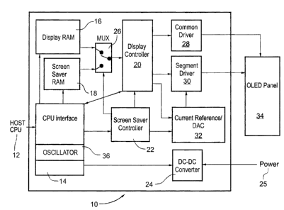
Turning to Figure 1, a diagram illustrating a single integrated circuit (IC)
implementation of an Organic Light Emitting Diode (OLED) driver is shown. The
driver
is connected to a host central processing unit (CPU) 12 via a CPU interface
14. The
-2a-
CA 02481923 2004-09-16
CPU interface 14 is connected to a display random access memory (RAM) 16, a
screen
saver RAM 18, a display controller 20, a screen saver controller 22 and a DC-
DC
converter 24 which, in turn, is connected to a power source 25, generally in
the form of a
battery. The interface 14 also includes an oscillator 36 to provide timing for
the driver 10.
The display RAM 16, the screen saver RAM 18 and the screen saver controller 22
are connected to a multiplexer (MUX) 26 which is connected to the display
controller 20.
The display controller 20 is connected to a common driver 28, a segment driver
30 and a
current reference/digital-to-analog converter (DAC) 32. The combination of the
display
controller 20, the common driver 28 and the segment driver 30 may be seen as
display
controlling means for controlling the screen saver. The screen saver
controller 22 is also
connected to the display controller 20 and the current reference/DAC 32 while
the current
reference/DAC 32 is connected to the segment driver 30. Both the common driver
28 and
the segment driver 30 are connected to an Organic Light Emitting Diode (OLED)
panel
34.
The CPU interface 14 provides an interface between the driver 10 and the host
CPU 12 and defines the timing of generic interface signals such as READ,
WRITE, CHIP
SELECT, ADDRESS LINE(S), DATA LINES, and RESET. The display RAM 16 is
preferably SRAM and is used to store an image which is displayed on the OLED
panel 34
during an operating mode. In operation, the CPU interface 14 loads the display
RAM 16
based on data received from the host CPU 12. The screen saver RAM 18 is
functionally
similar to the display RAM 16 but has limited memory to store a screen saver
image from
the host CPU 12. For example, the screen saver RAM 18 may only hold data for a
20 x 20
pixel area even though the pixel area of the panel may be a 220 x 176 pixel
area.
The MUX 26 is a switch that selects the source of the image data to be
displayed
on the OLED panel 34. Therefore, in the operating mode, the MUX 26 provides a
connection between the display RAM 16 and the display controller 20 for image
retrieval
while in a screen saver mode, the MUX 26 provides a connection between the
screen saver
RAM 18 and the display controller 20 for image retrieval.
The display controller 20 reads the display image data from the display RAM 16
or
the screen saver RAM 18 (depending on its connection via the MUX 26) one row
at a time
and displays the data and provides the timing for the row of image data to be
displayed on
the OLED panel 34. The display controller 20 then retrieves the next row of
image data
stored in the display RAM 16 or screen save RAM 18, depending on which mode
the
-3-
CA 02481923 2004-09-16
OLED panel 34 is in. This process is repeated several times per second until
the entire
image is displayed on the panel 34. The display controller 20 also defines
where the
display image data from the display RAM 16 or screen saver RAM 18 is mapped
onto the
OLED panel 34. For example, the host CPU 12 may transmit a command to the
display
controller 20 to only display the first fifty lines of image data and leave
the rest of the
panel 34 blank, or black.
The screen saver controller 22 is used to control the screen saver so that the
host
CPU 12 does not have as much of a burden. The screen saver controller 22 also
controls
the MUX 26 as will be described below with respect to Figure 2 which is a
schematic
diagram of the screen saver controller 22.
The common driver 28 sends pulses to indicate to the OLED panel 34 the address
to which the segment driver 30 is currently sending the image data.
Furthermore, the
segment driver 30 converts the digital data from the display RAM 16 or screen
saver RAM
18 to a current level required to drive the OLED panel 34 at a defined level
(pixel
luminance). The display RAM 16, via the display controller 20, defines this
pixel
luminance level and transmits this level to the current reference/DAC 32. The
current
reference/DAC 32 typically includes a DAC for each of red, green, and blue for
a colour
display. The DC-DC converter 24 converts the power supply voltage 25,
typically 3 V, to
a level required by the OLED panel 34.
Turning to Figure 2, a schematic block diagram of the screen saver controller
22 is
shown. The screen saver controller 22 comprises a set of RGB timers 35 seen as
a RED
timer comprising a RED preset 36 and a RED down counter 38, a GREEN timer
comprising a GREEN preset 40 and a GREEN down counter 42 and a BLUE timer
comprising a BLUE preset 44 and a BLUE down counter 45. The screen saver
controller
22 also includes a screen saver timer comprising a screen saver down counter
46 and a
move icon timer comprising a move icon down counter 48, along with various AND
and
OR gates. The move icon down counter 48 is also connected to a command
generator 53
which is connected to the display controller 20. The move icon down counter 48
provides
a timer for determining when the location of the screen saver image is to
change.
Inputs to the screen saver controller 22 include a clock source 50 originating
from
the oscillator 36 in the CPU interface 14 and inputs 70, 72 and 90 from the
CPU interface
14.
-4-
CA 02481923 2004-09-16
The command generator 53 generates and transmits two types of commands for the
display controller 20. These two commands are image size and start address
(image
location). The generated start address of the image display is randomly
changed each time
the move icon down counter 48 reaches zero so that the screen saver image is
constantly
moving on the OLED panel 34 in order to preserve the primary colours. The
image size
that is generated and transmitted by the command generator 53 is based on the
size of the
screen saver RAM 18 or may be determined to be a smaller size by the command
generator 53. In a preferred embodiment, the image size for the screen saver
is a 20 x 20
pixel area.
Each of the RGB timers is used to control one of the primary colours of the
OLED
panel 34, to compensate for differential aging of the colours, and is loaded
based on values
received from the host CPU 12 via the CPU interface 14. Each of the down
counters
includes a load input 54, an enable input 56, a zero output 58 and. a clock
input 60. The
clock input 60 of each down counter 38, 42, and 45 receives its input from the
clock
source 50.
The enable input 56a of the RED down counter 38 receives the input 70 from the
CPU interface 14 while the zero output 58a of the RED down counter 38 is
connected to
the enable input 56b and the load input 54b of the GREEN down counter 42. The
zero
output 58b of the GREEN down counter 42 is connected to the load input 54c and
the
enable input 56c of the BLUE down counter 45. The load input 54a of the RED
down
counter 38 is loaded with the result from the ORing of the zero output 58c of
the BLUE
down counter 45 and the zero output 58d of the screen saver down counter 46.
The result of ANDing the input 70 from the CPU interface 14, the zero output
58a
of the RED down counter 38 and the zero output 58d of the screen saver down
counter 46
controls a disable RED DAC signal 62 while the result of ANDing the input 70
from the
CPU interface 14, the zero output 58b of the GREEN down counter 42 and the
zero output
58d controls a disable GREEN DAC signal 64 and the result of ANDing the input
70 from
the CPU interface 14, the zero output 58c of the BLUE down counter 45 and the
zero
output 58d of the screen saver time out 46 controls a disable BLUE DAC signal
66. As
described The load input 54d and the enable input 56d for the screen saver
down counter
46, along with the enable input 56e of the move icon down counter 48 receive
their input
from input 72 transmitted by the CPU interface 14.
-5-
CA 02481923 2004-09-16
The zero output 58d of the screen saver down counter 46 is connected to the
MUX
26 and the command generator 53. The zero output 58e of the move icon down
counter 48
is also connected to the command generator 53.
In operation, the mobile electronic device OLED panel 34 generally is in one
of
two operating modes. Mode 1 may be defined the operating mode for the panel
whereby
the user is interacting with the mobile electronic device while mode 2 is the
screen saver
mode. As will be understood by one skilled in the art, in mode 1, the host CPU
12
accesses and changes the image data stored in RAM 16 as required by a software
application executing on the host CPU 12 of the mobile electronic device.
After receiving
a signal from the CPU interface 14, the display controller 20 retrieves a row
of image data
via the MUX 26 (which connects the display controller 20 to the display RAM 16
in mode
1) and transmits a row of the image data to the segment driver 30. After
determining the
location on the panel for the image data and receiving a pulse from the common
driver 28,
the segment driver 30 then transmits the row of image data to the OLED panel
34. This
process is repeated for each row of the image and continues to be repeated to
maintain the
image on the OLED pane134. Once the image has been displayed on the panel, the
CPU
interface 14 initiates the screen saver down counter 46 by transmitting a
signal to the load
input 54d of the screen saver down counter 46. This value is loaded into the
screen saver
down counter 46 any time there is activity on the CPU interface 14 or if a row
of image
data from the display RAM 16 is transmitted to the OLED panel 34. This value
is
decremented after each clock pulse and if the value is decremented to zero,
the mobile
electronic device and the display panel enter the screen saver mode.
Turning to Figure 3, a flow diagram of a method of providing a screen saver
for a
mobile electronic device is shown. Firstly, a check is performed to determine
if there is
any CPU interface activity. For example, when a WRITE line toggles, the screen
saver
down counter 46 is reloaded. The screen saver down counter 46 decrements with
every
pulse of the clock signal 50 from the CPU interface 14. As long as the screen
saver down
counter 46 has not reached zero and CPU activity is sensed, the mobile
electronic device
remains in mode 1. When the screen saver down counter 46 reaches zero, it is
detected at
step 102 that the screen saver time out has elapsed. In this event, there has
not been any
activity on the CPU interface during the allotted time period and the screen
saver down
counter 46 has not been reloaded, indicating a need to change from the
operating mode to
the screen saver mode. The screen saver down counter 46 then sends a signal
via its zero
-6-
CA 02481923 2004-09-16
output 58d to the MUX 26 to switch the connection for the display controller
20 from the
display RAM 16 to the screen saver RAM 18 so that the display controller 20
retrieves the
image data from the screen saver RAM 18 (step 104). The signal from the zero
output
58d is also transmitted to the command generator 53 to generate its two
commands.
In mode 2, the image on the display 34 is preferably black, or not powered
except
for the small image area. The image data is stored in the screen saver RAM 18.
The
image data is retrieved from the screen saver RAM 18 (step 106) by the display
controller
20 and the display location for the screen saver image is also determined by
the display
controller 20 (step 108) via the command generator 53 and displayed on the
panel 34 (step
110) as described above with respect to the display RAM 16. The displayed
location of
the screen saver image is not fixed and randomly (or in accordance with pre-
defined
movements) moves around the panel as defined by the command generator 53 and
the
move icon down counter 48. The movement of the screen saver image allows the
primary
colours of the OLED panel 34 to age uniformly. In addition to the screen saver
image
moving, in a preferred embodiment, the colour of the screen saver image
changes at a rate
defined by the RGB timers 35. These timers 35 are programmed to match the life
of the
three primary colours of the OLED panel.
Once the move icon down counter 48 is enabled, the start address of the screen
saver image changes every time the move icon down counter 48 reaches zero. The
counter is initially set by the input 90 from the host CPU 12 via the CPU
interface 14 and
decremented with each clock pulse when the mobile electronic device and
display panel
are in the screen saver mode. When the move icon down counter 48 reaches zero,
the
move icon timer has elapsed (step 112), and a signal is transmitted from the
zero output
58e of the move icon down counter 48 to the command generator 53 which
generates a
new address for the image to be displayed on the OLED panel 34. This new
address is
then transmitted to the display controller 20 and the screen saver image is
retrieved (step
106). If the move icon timer has not elapsed, a check is performed to verify
that the
colour aging is enabled (step 114). If not, a check is then performed to
verify CPU
interface activity (step 100). In the absence of interface activity, steps
112, 106-110 if
necessary, and 114 are repeated. Where interface activity is detected, screen
saver mode is
exited, as shown at 101.
If colour aging is enabled, all the DACS are turned off (step 115) until the
RED,
GREEN and BLUE down counters 38, 42, and 45 are loaded and enabled. The RED,
-7-
CA 02481923 2004-09-16
GREEN and BLUE down counters 38, 42, and 45 are then used to control the
relative
aging factor for these panel colours. In a preferred embodiment, the RED DAC
and the
RED counter 38 are enabled (step 116) by inputs 70 and 90 from the host CPU
and the
ORing of the zero signal 58d from the screen saver down counter 46 and the
zero signal
58c from the BLUE down counter 45. When the RED down counter 38 reaches zero,
a
signal from its zero output 58a is transmitted to an AND gate along with the
input 70 from
the CPU interface 14 and the signal from the zero output 58d of the screen
saver down
counter 46, and the RED DAC disable signal 62 disables the RED DAC (step 118).
The
signal from the zero output 58a is also transmitted to the enable input 56b of
the GREEN
down counter 42 to enable the GREEN DAC and the GREEN timer (step 120). When
the
GREEN down counter 42 decrements to zero, a signal from its zero output 58b is
transmitted to an AND gate along with the input 70 from the CPU interface 14
and the
signal from the zero output of the screen saver down counter 46, and the GREEN
DAC
disable signal 64 disables the GREEN DAC (step 122). The signal from the zero
output
58b is also transmitted to the enable input 56b of the BLUE down counter 45 to
enable the
BLUE DAC and the BLUE timer (step 124). Once the BLUE down counter decrements
to
zero, a signal from its zero output 58c is transmitted to an AND gate along
with the input
70 from the CPU interface 14 and the signal from the zero output of the screen
saver down
counter 46, and the BLUE DAC disable signal 66 disables the BLUE DAC (step
126).
The signal from the zero output 58c is also transmitted to the OR gate and
coupled with
the signal from the zero output 58d of the screen saver down counter 46. The
result of this
ORing is then transmitted to the load input 54a of the RED down counter 38.
This process
continues until the CPU interface re-loads the screen saver down counter 46
via the load
signal 54d, which results in the screen saver down counter 46 and the zero
output 58d
being asserted, which enables all three DACs.
As will be understood, there are many different implementations and methods
for
driving an OLED panel 34. Other OLED drivers may use external RAM or have a
common and segment IC as a separate component. Furthermore, in other
embodiments,
the screen saver controller may be included within the display controller 20.
It will also be understood that although step 100 is shown as a separate step
that
follows other steps in the method shown in Fig. 3, interface activity
preferably interrupts a
screen saver mode, such that screen save mode is exited upon detection of
activity.
-8-
CA 02481923 2004-09-16
In another embodiment of the invention, data, such as the time data, system
status
data or the number of unread email data, may be displayed in the screen saver
image
The above-described embodiments of the present invention are intended to be
examples only. Alterations, modifications and variations may be effected to
the particular
embodiments by those of skill in the art without departing from the scope of
the invention,
which is defined solely by the claims appended hereto.
-9-