Note: Descriptions are shown in the official language in which they were submitted.
CA 02482058 2004-09-17
30513-4
TITLE OF THE INVENTION
Method of Fabricating Semiconductor Components
Through Implantation and Diffusion in a Semiconductor
Substrate
FIELD OF THE INVENTION
The invention relates to a method for fabricating
semiconductor components in a semiconductor substrate by
forming wells with different conductivity types and forming
trench structures in the substrate.
BACKGROUND INFORMATI~N
A well is a three-dimensional region or portion of
a semiconductor substrate, having major~_ty charge carriers
of a different conductivity type (for example P-type) in
comparison to the majority charge carriers of the
surrounding portion of the substrate around the well (for
example N-type). As a result, blocking or non-conductive
PN-junctions will be formed along the peripheral edges or
boundaries of the well, in connection with a suitable
electrical reverse-biasing thereof, whereby these PN-
junctions effectively electrically isolate the interior of
the well from the surroundings thereof.
Various semiconductor devices include different
types of trench structures in a semiconductor substrate.
For example, such trenches are used for electrical isolation
of so-called component boxes, pockets or tubs in the depth
and/or on the surface of the semiconductor substrate. As a
further example, such trenches are used for the three-
dimensional formation or configuring of electrically active
regions such as a trench capacitor or a transistor drift
zone within the semiconductor substrate. Generally, deep
1
CA 02482058 2004-09-17
30513-4
trenches are used to achieve electrical isolation in the
depth direction, while shallow trenches are preferred for
achieving the three-dimensional formation or configuration
of electrically active regions and also for electrical
isolation purposes on the surface of the substrate. Deep
trenches and shallow trenches are differ_entiated,from one
another by the aspect ratio of the depth relative to the
width thereof. Deep trenches have an aspect ratio of
greater than one and shallow trenches have an aspect ratio
of less than or equal to one. In other words, deep trenches
are deeper than they are wide, while shallow trenches are as
wide as or wider than they are deep.
It is generally known in the art to form wells and
trenches as mentioned above, as well as various active
regions within a semiconductor substrate to form a
semiconductor device. Examples of such active regions
include individual transistors that are integrated into the
same common substrate. The individual active regions are
separated from one another by field areas or field regions,
so that the surface of the semiconductor substrate can be
divided into active regions and field regions that are
complementary to each other.
A'device fabrication method incorporating the
above features is known, for the specia7_ case of fabricating
a DMOS-transistor as a semiconductor element, from the
German Laying-Open Publication DE 101 31_ 705 A1, as well as
the counterpart US Patent 6,780,713 (Bromberger et al.), the
entire disclosure of which is incorporated herein by
reference.
The above mentioned field regions are provided
with insulating or isolating structures in order to avoid an
2
30513-4
CA 02482058 2004-09-17
undesired drift of charge carriers, i.e. electrons or holes,
between the respective ac ive regions. In integrated
circuits based on silicon technology, it is known to isolate
respective active regions on the surface of the device or
circuit from each other by means of an insulation structure
consisting of a silicon oxide, generally called a field
oxide.
On the other hand, active regions are isolated
from one another in the depth of the structure of the
integrated circuit by means of the deep trenches mentioned
above, or alternatively or additionally by well regions or
wells used for the lateral isolation. Such wells are
typically produced through implantation of a dopant followed
by thermally supported diffusion of the dopant into the
semiconductor substrate. Since the diffusion is generally
not directional, i.e. does not proceed along a preferred
direction, the diffusion typically occurs both in the depth
direction as well as in the width or lateral direction.
Thus, the lateral spreading of the wells will become ever
greater as the wells are to be diffused or driven deeper
into the semiconductor substrate such-as silicon, by a high
temperature well drive step. In other words, as the dopant
is diffused deeper into the substrate it necessarily also
spreads wider in the lateral direction. As a result, the
mutual influence or interference of adjacent wells or
adjacent regions due to out-diffusion will also increase.
In this regard, the term "out-diffusion'N refers to a
reduction of a net concentration of the dopants along the
peripheral edge or boundary of a well;due to a lateral
diffusion of dopants out of an oppositely doped adjacent or
neighboring well. Thus, the net dopant concentration of the
intended dopant type of a given well falls off or diminishes
3
CA 02482058 2004-09-17
30513-4
toward the lateral boundaries thereof adjacent to a
neighboring well of opposite dopant polarity.
In the fabrication method known from the above
mentioned German Patent Laying-Open Publication DE 101 31
705 A1, respective well regions are defined through an
implantation of dopants into areas near the surface of the
substrate, followed'by a complete in-diffusion, i.e.
diffusion of the dopant into the substrate volume by a
thermal drive-in step, before the further subsequent
formation of deep trenches that will def-_ine component boxes
isolated from each other within the substrate. Still
further in the known method according to the German
Publication mentioned above, another trench structure is
formed by a Shallow Trench Isolation (STI) etching process,
and then a separate doping of the boundaries (walls and
floor) of the trench is carried out to form a drift zone of
the DMOS-transistor.
The above mentioned conventional process of
defining the wells before forming trenches can unfortunately
suffer the effects of the above discussed out-diffusion,
especially if high dopant concentrations and/or deep
diffusion penetration depths are to be achieved. In order
to avoid or prevent such undesired influences of out-
diffusion along the respective boundaries of neighboring
well regions of opposite conductivity type, the spacing
distance between electrically active reeJions with different
well dopings must be selected sufficiently large so that the
respective dopant species do not out-diffuse and thus
counteract the intended doping in the neighboring well
region. However, such a large spacing distance between
differently doped well regions undesirably limits the
packing density of device structures per surface area. In
4
CA 02482058 2004-09-17
° 30513-4
other words, the lateral spacing of the well regions from
each other to avoid the undesirable influences of out-
diffusion mutually between neighboring wells requires a
corresponding minimum lateral width of the total device
structure, which necessarily limits the possible size-
reduction or miniaturization of the device.
StJI~IARY OF THE INVENTION
In view of the above, it is an object of the
invention to provide a method of fabricating a semiconductor
component in a semiconductor substrate while enabling a
further size reduction or miniaturization of the device
structure. More particularly, it is an objet of the
invention to provide such a semiconductor component
fabrication method that avoids or reduces the undesirable
out-diffusion or diffusion interference between neighboring
well regions of different conductivity type. The invention
further aims to avoid or overcome the disadvantages of the
prior art, and to achieve additional advantages as apparent
from the present specification. The attainment of these
objects is, however, not a required limitation of the
claimed invention.
The above objects have been achieved according to
the invention in a method of fabricating a semiconductor
component in a semiconductor substrate comprising.steps of
forming first and second wells with opposite conductivity
type in the semiconductor substrate, forming at least one
trench in the semiconductor substrate, as well as forming
and electrically contacting active regions in the
semiconductor substrate. Mora particularly, forming the
wells comprises implanting respective do>pants for the first
and second wells into the semiconductor substrate, and then
5
CA 0248205 8 2004-09-17
30513-4
carrying out at least one first diffusion through a first
high temperature drive step before form_i.ng the at least one
trench, followed by at least one second diffusion through a
second high temperature drive step after forming the at
least one trench.
The inventive method divides the high temperature
treatment for diffusing dopants into the wells into two
separate high temperature drive steps for carrying out two
separate diffusions, namely one before and one after forming
the trench(es). This serves to reduce or avoid the problems
of out-diffusion or interfering diffusion of opposite dopant
species from neighboring oppositely-doped well regions as
discussed above.
This advantage of the invention must be understood
further in connection with a balancing of another and
somewhat-contrary advantage; as follows. For purposes of
this comparative discussion, one could consider carrying out
the diffusion of the well doping entirely after the
formation of trenches, in order to thereby avoid or prevent
the above-mentioned problem of out-diffusion in the outer
edges or boundary areas of the respective well. On the
other hand, however, if the deep trenches are etched before
carrying out the high temperature drive step for diffusing
the dopants into the wells, this would fundamentally aive
rise to the problem that defects can be generated along the
edge or boundary of the isolation trench due to the high
thermal loading that arises during the subsequent thermal
drive step for achieving the entire dopant diffusion. In
the subsequent operation of the semiconductor device, such
defects can lead to undesirable leakage currents, which in
turn undesirably reduce the breakdown voltage of the device.
6
CA 02482058 2004-09-17
30513-4
Thus; in view of the above mentioned competing or
contrary considerations, the inventive method aims to
provide an acceptable or even optimized compromise between a
substantial reduction or avoidance of the out-diffusion of
oppo ite dopants in the outer edges or boundary areas of
neighboring wells on the one hand, and an avoidance of
defects to prevent exceeding critical leakage current rates
in the later operation of the fabricated device on the other
hand. In this regard; the first requirement arises from the
urge to achieve a further size reduction of the device
structure, while the second requirement arises from the
demand to achieve a high breakdown resistance. These two
opposite requirements are, achieved in an optimized balanced
manner through the inventive division of the high
temperature thermal drive steps for carrying out the
diffusion of the well doping into two separate high
temperature diffusion drive steps that are separated in time
from one another, namely at least one such step before and
at least one such step of er the formation of trench
structures. Thereby; the problem of out-diffusion is
reduced or avoided, while still reducing the temperature
loading of the structure after the formation of trenches.
In a preferred embodiment of the invention, at
least one (or some) of the trench structures is a deep
trench that mutually electrically isolates component boxes
(also called pockets or tubs) formed within the
semiconductor substrate. Irz this manner, the lateral
diffusion of well dopants through the trench structures is
limited. Thereby, small well regions with high dopant
concentrations and/or dopant concentrations that penetrate
deeply into a volume of the semiconductor substrate can be
produced, without giving rise to an undesired lateral out-
diffusion problem along the edges or lateral boundaries of
CA 02482058 2004-09-17
30513-4
the wells. More particularly, such an undesired lateral
diffusion is prevented by the interposed trenches:
It is further preferred that the deep trenches
extend all the way down to an insulating layer on which the
semiconductor substrate is disposed. Thereby, the
neighboring wells are not only separated and isolated from
one another in a defined manner at the surface of the
semiconductor substrate, but also deeply within the volume
of the semiconductor substrate.
According to another preferred embodiment of the
invention, at least one (or some) of the trench structures
is a shallow trench that at least partially bounds and
serves to define a drift zone of a DMOS-transistor. In
comparison to a typical Metal Oxide Semiconductor (MOS)
transistor, a DMOS-transistor is distinguished in that it
additionally has a drift zone, i:e. a zone in which the
motion of the charge carriers is caused or effected only by
an electrical field prevailing between t;he opposite ends of
this zone. This drift zone is provided between an edge of a
control gate and a drain region of the transistor. The
lateral size or extension of the drift zone can be reduced
by forming the drift zone along the boundaries (i.e.
especially the sidewalk) of a shallow trench.
A further preferred feature of the invention is
that the shallow trench is formed through a Shallow Trench
Isolation (STI) process. In the STI technology, a shallow
trench is formed by an anisotropic etching process between
active regions covered with a nitride protective layer, and
then the etched trench is filled with an insulating material
such as silicon dioxide or polysilicon. Using the STI
technology, for example, higher packing densities can be
8
CA 02482058 2004-09-17
30513-4
achieved in comparison to the use of a V-trench etching with
a LOCOS (LOCal Oxidation of Silicon) mask.
It is also preferred that the sidewalk and/or
floor region of the respective trench ar_e doped separately
and independently. Thereby, the dopant profile of the drift
zone can be optimized with respect to desired
characteristics such as a high breakdown voltage, a low
turn-on voltage, and a RESURF (REduced SURface Field)
effect. This separate or individualized doping of different
portions of the drift zone is preferably carried out through
at least one implantation of a drift zone dopant before the
second high temperature drive step and a diffusion of the
implanted drift zone dopant during the second high
temperature drive step. Thereby, a portion of the diffusion
of the well doping is carried out purposely in a targeted
and controlled manner in common with a diffusion of the
drift zone doping. As a result, the method can omit a
separate high temperature drive step for diffusing the drift
zone dopant, so that the total process duration, thermal
load, complexity, and cost can be reduced. In connection
with the inventive division and sequencing of the diffusion
steps of the well dopant, it is thereby also possible to
optimally adjust the doping in the region of the drift zone
of the DMOS-transistor under the shallow trench formed
through the STI process.
It is also preferred according to the invention
that a first well region into which a first dopant has been
implanted, and a second well region into which a second
dopant has been implanted; are laterally spaced from one
another. Furthermore; the diffusion steps are then carried
out in such a manner so that a region of intrinsic
conductivity or base doping of the semiconductor substrate
9
CA 02482058 2004-09-17
30513-4
material (i.e. a region without the additional well doping)
remains between the first and second well regions after
completion of the high temperature drive steps. These
features of the invention, individually or in combination
with one another, reduce a compensation of the various
different dopings of neighboring well regions in an inward
direction, and thus contribute to the desired increase of
the breakdown voltage to a level of more than 80 V.
In another preferred feature of the invention, the
trenches are filled with a dielectric material; which
preferably comprises an oxide of the semiconductor substrate
material, a nitride of the semiconductor substrate material,
a polycrystalline material of components or elements of the
semiconductor substrate material, or a mufti-layered system
of any one or more of the above mentioned materials. These
materials each have a good electrical insulating effect and
readily form good joints with the maternal of the
semiconductor substrate, being sufficiently temperature
resistant, and insensitive to oscillation or vibrations and
thus being durable and having a good fatigue strength.
Further advantages of the invention are evident
from the remainder of the specification and the accompanying
drawings. It should be understood that the features and
characteristics disclosed herein cannot only be used in the
respective disclosed combinations, but also can be used in
other combinations or even individually while still
remaining with the scope of the present invention.
BRIEF DESCRIPTION OF THE DRAWINGS
Tn order that the invention may be clearly
understood, it will now be described in connection with
CA 02482058 2004-09-17
30513-4
example embodiments thereof, with reference to the
accompanying drawings, wherein:
Fig. 1 is a schematic cross-section of a
semiconductor substrate during a step of implanting a first
dopant;
Fig. 2 'is a schematic cross-section of the
semiconductor substrate after the implantation of dopants as
the basis for defining two wells in the substrate;
Fig. 3 is a schematic cross-section of the
semiconductor substrate after a first high temperature
diffusion drive step for carrying out a partial diffusion of
the well dopants;
Fig. 4 is a schematic cross-section of the
semiconductor substrate after performing a deep trench etch,
and at the beginning of a second high temperature diffusion
drive step;
Fig. 5 is a schematic cross-section of'the
semiconductor substrate after completing the second high
temperature diffusion drive step and further steps for
forming and contacting active regions of a semiconductor
component;
Fig. 6 is a schematic cross-section of a
semiconductor substrate generally similar to'Figs. 1 and 2,
but showing a first optional intermediate step for
fabricating a DMOS-transistor with a drift zone to be
defined and bounded along a shallow trench;
Fig. 7 is a schematic cross-section of the
semiconductor substrate according to Fig. 6, showing a
11
CA 02482058 2004-09-17
30513-4
further associated second intermediate step of forming the
shallow trench;
Fig. 8 is a schematic cross-section of a
semiconductor substrate according to Fig. 2 showing a
further optional intermediate step for producing a doped
drift zone of a DMOS-transistor; and
Fig. 9 is a schematic cross-section showing the
semiconductor substrate of Fig. 8 after the completion of
further associated steps for forming the DMOS-transistor.
DETAILED DESCRIPTION OF A PREFERRED E~~AMPLE EMBODIMENT AND
OF THE BEST MODE OF THE I1WENTION
Fig. l schematically shows a cross-section of a
portion of a semiconductor body l0 comprising a
semiconductor substrate 12 onan insulating intermediate
layer or isolating layer 14. A typical example of such a
semiconductor body l0 is represented by a "Silicon On
Insulator" (SOI) wafer. In this regard, the insulating
intermediate layer 14 is typically realized as a silicon
dioxide layer.
As a first step in a device or component
fabrication process, respective well regions with different
conductivity type will be formed in the semiconductor body
10. Namely, for forming these well regions with respective
different conductive y of the respective majority charge
carriers, different partial regions of the semiconductor
substrate 12 will re pectively be doped with dopants of
different valence, so that the different conductivity types
result in the respective well regions. To achieve a P-type
conductivity in a four-valent semiconductor substrate
material such as silicon, for example, boron atoms, which
12
30513-4
CA 02482058 2004-09-17
are incorporated as three-valent substitution defect sites
in the silicon lattice; and which act a.s electron acceptors;
are doped into the silicon material. Analogously, an N-type
conductivity is achieved by doping, for example, a four-
s valent semiconductor substrate with arsenic or phosphoric
atoms, which are incorporated as five-valent substitution
defect sites in the basic crystal lattice formed of four-
valent silicon atoms, and which act as electron donors.
For spatially defining the areas of the well
regions to be formed, areas that are not be doped are
covered by a mask l6. The mask 16 is patterned and/or
provided with openings in any conventionally known manner.
Basically in principle the dopants can be introduced into
the regions'of the semiconductor substrate 12 not covered by
the mask l6 either by a diffusion technique or by an ion
beam implantation. In modern semiconductor device
fabrication processes, the ion beam implantation is
generally preferred,, whereby an exactly controlled quantity
of dopant atoms is initially ionized uniformly and
accelerated to a defined ion velocity to form an ion beam 18
of the ionized dopant atoms as indicated. schematically by
the arrows in Fig. 1.
The ion beam 18 of dopant ions impinges on areas
of the semiconductor substrate 12 not covered by the mask
16. The dopant ions then penetrate into the crystal lattice
of the semiconductor substrate material. There, the ions
are retarded or decelerated until coming to a stop and
respectively being received at a substitution defect site
within the lattice. The penetration depth of the respective
ions into the semiconductor substra a 12 depends on the
kinetic energy of the ions in the ion beaml8, as well as
other factors such as the composition, crystal structure,
13
CA 02482058 2004-09-17
30513-4
crystal orientation, and the like of th.e semiconductor
substrate 12. Due to the release of energy from the ions as
they penetrate into the semiconductor crystal lattice, the
ions damage the crystal lattice structure and typically come
to rest at'respective interstitial lattice locations. This
implantation step forms a surface layer 20 of the
semiconductor substrate 12 having the dopant ions implanted
and doped therein. Due to the above mentioned lattice
damage of this surface layer 20 caused by the ion
implantation, it is then necessary to carry out a thermal
annealing, curing and activating step at an elevated
temperature in order to remove or repair the defects or
crystal damage, and to relocate the dopant atoms as much as
possible to lattice sites in the volume of the semiconductor
substrate 12. It is a significant characterizing feature of
the present invention, that these thermal annealing and
activating steps are preferably not all performed directly
after the implantation, but rather at. least some of such
steps are performed only after further structuring steps
have been carried out.
In Fig. 1, the relatively thin. surface layer 20
represents the surface layer of the semiconductor substrate
12 that has been enriched with dopant atoms through the
preceding implantation. In that regard, the sectional
hatching of the layer 20, with diagonal lines extending from
the bottom left to the top right represents a particular
conductivity type of the dopant, for example a P-type
conductivity. Also, the relatively dense or close
arrangement of the sectional hatch lines represents a
relatively high dopant concentration:
Fig. 2 shows the semiconductor body l0 of Fig. 1
after the implantation of different dopants of different
14
CA 02482058 2004-09-17
30513-4
polarity as the basis for, defining two well regions in the
semiconductor substrate l2. Namely, the first surface layer
20 with a P-type conductivity has been formed by the first
ion implantation step as described above in connection with
Fig. l, and then a second oppositely (N-type) doped surface
layer 22 has been additionally formed. This involves
carrying out a further masking step to cover the first
surface layer 20 with a further mask, and then a second ion
implantation through the open or exposed area of the second
mask to form the second surface layer 22 doped with
implanted ions of the second conductivity type, e.g. N-type
conductivity, which is represented by the diagonal sectional
hatch lines extending from the upper left to the lower right
in the surface layer 22 in Fig. 2.
The surface layer 22 is prefez°ably located and
formed so that an undoped or un-implanted lateral spacing
distance 24 remains between the first surface layer 20 and
the second surface layer 22. In this lateral spacing
distance 24; the original, e.g. intrinsic, state of the
semiconducting material of the semiconductor'substrate 12
remains, without implanted well dopants. Alternatively; the
twa surface layers 20 and 22 could be directly adjoining one
another, or may even overlap one another in a partial
overlapping region. ,In this case, the donor and acceptor
dopant atoms of the two surface layers would neutralize or
cancel each other out in the overlapping region (to the
extent that the dopant concentrations are the same).
The mask or masks 16'used for spatially limiting
and defining the implantation steps as discussed above can
be made of, for example, any dielec ric material or
materials, such as silicon oxide and silicon nitride, that
are also known for use in connection with diffusion
CA 02482058 2004-09-17
30513-4
techniques. However, the ion deceleration or retardation in
solid bodies, in contrast to the diffusion process, is not a
thermodynamic, but rather essentially a mechanical process.
Thus, essentially any material that achieves such a
mechanical blocking, deceleration or retarda ion of the ions
can be used for the ion implantation mask. Since high
temperatures do not arise during the ion implantation, it is
especially possible to use a photographically exposed and
developed photoresist layer as the mask 16, i.e. as a
protective layer to spatially limit and define the areas of
ion implantation. Since no separate elevated temperature
steps are needed for producing protective layers in
connection with a mask l6 consisting of photoresist, as
would otherwise be necessary in connection with the
deposition of oxides and/or nitrides for example, the total
wafer processing time and the thermal loading of the wafers
are minimized.
For the above reasons; the masks 16 are preferably
defined lithographically as photoresist layers. Through an
etching step, the exposed or unexposed resist window areas
are etched free to the surface of the semiconductor
substrate 12. Then, the exposed surface of the
semiconductor substrate l2 is covered with a scattering
oxide, and then the doping,is carried out by means of the
ion implantation as described above.
As an alternative to the above described process,
the semiconductor body l0 is first covered with an oxide
that will later serve as an implantation mask' during the
implantation doping of the well regions. In that regard,
the well regions are lithographically defined with masks in
a photoresist layer . A wet chemical etching step opens the
oxide in the resist windows, down to the silicon surface.
16
CA 02482058 2004-09-17
30513-4
Then, after covering the free or exposed silicon surface
with a scattering oxide, the doping is carried out by means
of the ion implantation.
After the ion implantation, a first high
temperature step is carried out to perform the partial or
incomplete drive-in'diffusion 26 of the dopant ions from the
surface layers 20 ahd 22 deeper into the semiconductor
substrate 12, so as to begin (partially) to form the first
well 32 and the second well 34. The result of this first
high temperature thermal drive step is shown in Fig. 3,
wherein the first drive-in diffusion 26 has penetrated the
dopant ions to a penetration depth 28 corresponding to about
half (e.g. 40% to 600) of the total depth of the
semiconductor substrate 12. The arrows of the diffusion 26
in Fig. 3 represent the main diffusion direction, whereby it
should be understood that a diffusion also takes place in a
lateral direction. Generally, the temperature and the
duration of the first high temperature thermal drive step
are preferably defined or selected so that the penetration
depth 28 of the dopants in this first step amounts to about
one-quarter to three-quarters of the total penetration depth
of the doped wells to be achieved through all of the high
temperature diffusion drive steps. The particular
temperature and duration to be used can be determined
empirically and/or experimentally, depending on the type and
other characteristics of the dopant and of the substrate
material.
The lateral spacing distance 24 between the first
and second surface layers 20 and 22 is preferably
dimensioned so that even after the first drive-in diffusion
26, an intermediate region 30 free of the well dopants wil l
remain between the first and second wells 32 and 34 that are
17
CA 02482058 2004-09-17
30513-4
being formed. If the semiconductor substrate 12 has an
intrinsic P-conductivity, or has been doped with a P-type
base doping, this intermediate region 30 is designated as a
P-body: As mentioned above, the P-body 30 will contribute
to increasing the breakdown voltage of the finished
component or device. It should b~ understood that the
conductivity types can be reversed in another example
embodiment.
While the above discussion details a single first
drive-in diffusion 26 carried out in a single first high
temperature step, it should be understood that the invention
is not limited in this regard. Namely, plural drive-in
diffusions can be carried out in one or more'high
temperature steps before the formation o f one or more trench
structures. In such a case, all of the drive-in diffusions
and all of the high temperature steps carried out before the
formation of trenches are regarded as "first" drive-in
diffusions and "first" high temperature steps. Similarly,
the following discussion will detail the performance of a
single second drive-in diffusion during a second high
temperature step, but the inventive process may
alternatively include plural "second" drive-in diffusions
carried out in one or more "second" high temperature steps
following the formation of trenches. Thus, the term "first"
high temperature step will refer to any high. temperature
step before the trench formation, while the term "second"
high temperature step will: refer to any high temperature
step carried out after the trench formation.
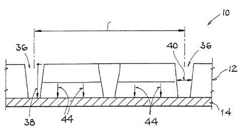
The process following the state of'Fig. 3 will now
be discussed in connection with Fig. 4. In a first example
embodiment of the inventive method, the next step involves
the formation of deep trenches 36 in the semiconductor
18
CA 02482058 2004-09-17
30513-4
substrate 12. In this cori ext, a trench 36,is regarded as
"deep" when it has a depth 38 greater than a width 40
thereof. Note that in Fig. 4, the trench width 40
represents the average width when the trench 36 has a
tapering cross-section. The deep trenches 36 are formed
either by a wet etching process or by a dry etching process
in connection with a masking step. When an SOI wafer is
used as the semiconductor body 10, the deep trenches 36
preferably reach all the way down the insulating layer 14,
and define respective mutually isolated component boxes,
also called pockets or tubs, that are bounded and isolated
from each other by the trenches 36, and in which various
active regions will later be formed in further method steps.
After the formation of the deep trenches 36 as
described above, at least one second high temperature
thermal drive step is carried out, in which the well dopants
for doping the wells 32 and 34 are fully or completely
thermally driven and diffused into the semiconductor
substrate 12. Thissubstantially complete second drive-in
diffusion 44 is represented by the corresponding arrows
showing the principle diffusion direction in Fig. 4. It can
also be seen that the diffusion additionallyprogresses
laterally, such that the P-body or intermediate region 30
free of the well dopants has a tapering or diminishing
width, as the wells 32 and 34 are diffused and spread
laterally along with the second diffusion 44 in the depth
direction. Preferably, the second high temperature step and
therewith the second drive-in diffusion 44 is carried out at
a temperature and for a duration sufficient so t-hat the
dopants defining the wells 32 and 34 are driven into the
semiconductor substrate 12 entirely to the insulating layer
14, so that he resulting wells 32 and 34 extend entirely
down to the insulating layer 14. In connection with a
CA 02482058 2004-09-17
30513-4
relatively small thickness of the semiconductor substrate 12
of an SOI wafer 10, this total penetration of the wells 32
and 34 provides the advantage of suppressing parasitic
capacitances.
The result of the second high temperature step for
performing the second drive-in diffusion 44 according to
Fig. 4 is shown in Fig. 5. The cross-sectional hatching
direction of the diagonal sectional lines in the wells 32
and 34 in Fig. 5, once again, represents the resulting
conductivit y type of the respective indicated region. In
the example illustrated iri Fig. 5, a first P-well 32 has
been formed on the left; and a second N--well 34 has been
formed on the right through the above first and second
diffusion processes 26 and 44. Ln that regard, the density
of the cross-sectional hatch lines is irn a reversed or
inverse relationship relative to the concentration of the
dopant atoms in the semiconductor substrate 12. While this
dopant atom concentration in the original implanted surface
layers 20 and 22 was still comparatively high, the
concentration of the dopants has been reduced by the
distribution and diffusion-spreading of the dopants through
almost the entire volume of the semiconductor substrate 12
within the respective component box 42.
The drive-in diffusion 44 in the second high
temperature phase is preferably carried out at such a
temperature and for such a duration, until a good uniform
distribution of the dopants up to the boundaries of the
trenches 36 has been established. The dopant atoms that
were initially positioned at interstitial lattice positions,
through the diffusion have been displaced to regular lattice
positions, whereby the dopant atoms are activated. This
process, as well as location or position exchange processes
CA 02482058 2004-09-17
30513-4
of the atoms of the host lattice, further achieve an
annealing and repairing of lattice defects or damage of the
host lattice of the semiconductor substrate 12 caused by the
original ion beam impingement.
At this stage of the process, adjacently located
component boxes 42 are in ulated or isolated from each other
at the bottom of the semiconductor substrate l2 by the
insulating layer 14, and through the depth of the
semiconductor substrate l2 by the deep 'trenches 36. In
order to achieve a good isolation also at the upper surface
of the semiconductor substrate 12, the trenches 36 are
subsequently filled with an insulating or dielectric
material 46, for example silicon dioxide, silicon nitride,
polysilicon, or a multi-layer system of anyone or more of
these materials. The filling of the trenches 36 through
oxidation can be carried out in parallel with the diffusion
44 during the second high temperature drive step for the
complete drive-in diffusion of the doparit atoms into the
depth of the semiconductor substrate 12,.
Fig. 5 schematically represents the result of the
above process steps in the semiconductor body 10 having
differently doped well regions 32 and 34 separated from one
another by an intermediate P-body 30 within a component box
or pocket 42. Through further doping steps according to any
conventionally known processes, preferably by implantation,
for example, a source connection 48, a gate connection 50 on
a gate oxide 52, and a drain connection 54 are produced in
order to fabricate a DMOS-transistor: It should be
understood that the fabrication of an actual complete DMOS
transistor can include further conventionally known steps,
such as a chemical mechanical polishing (CMP) planarization,
an extension implantation, a threshold voltage implantation,
21
CA 02482058 2004-09-17
30513-4
a gate oxidation, a gate poly-deposition and structuring
through a suitable mask step, further: mask steps for
carrying out lightly doped drain (LDD) implantations,
further mask steps for source/drain implantations, a boron
phosphorous silicate glass (BPSG) deposition; contact window
etching steps, and metallizations.
As a summary, the above described Figs. l to 5 set
forth a process sequence with the following steps.
Beginning with an SOI wafer as a starting material, a first
implantation is carried out to implant a P-well dopant and a
second implantation is carried out to implant an N-well
dopant, preferably with a lateral spacing distance 24
between the two dopant implantation areas. Then, a first
high temperature driving step for carrying out a first
partial drive-in diffusion 26 is followed by forming a deep
trench 36, which is further followed by a second complete
drive-in diffusion 44 in a second high temperature driving
step. This is followed by, or proceeds in parallel with,
filling the trench 36 with a dielectric material 46.
Finally, active regions are formed in the wells 32 and 34 to
produce a transistor.
Further alternative or optional embodiment
features of the invention will now be discussed in the
following with reference to Figs. 6 and ? as well as Figs. 8
and 9. These optional features relate to the fabrication of
a DMOS-transistor as a semiconductor component, having a
drift zone formed along the boundary of a trench without
individual doping (Figs. 6 and 7) or with individual doping
(Fig . 8 and 9) of the drift zone.
The embodiment according to Figs. 6 and 7
generally begins from the first and second steps described
22
30513-4
CA 02482058 2004-09-17
above with reference to Figs. l and 2. The details will not
be repeated here. After the implantation of the dopant into
the surface layers 20 and 22 according to Fig. 2, an
additional mask 56 is provided on the surface of the
semiconductor substrate 12 as shown in Fig. 6. This mask 56
can be either a resist mask or a hard mask, for example a
mask of silicon nitride: Next, the mask 56 is opened to
provide an opening 58 over the optionally present well-
dopant-free intermediate region 30 between the surface
layers 20 and 22, and a (preferably shallow) trench 60 is
formed through the opening 58, for example by an anisotropic
STI etching process, as shown in Fig. 7. According to the
STI (Shallow Trench Isolation) technique; after the shallow
trench 60 is formed by an anisotropic etching process
between the regions or areas covered by the mask 56, the
trench 60 is then later filled with an .insulating material
such as silicon dioxide or polysilicon.
In that context; a trench is regarded as a shallow
trench if it has an aspect ratio (i.e. a ratio of the trench
depth to the trench width) that is less than or equal to one
and preferably less than one. Among other things, the
trench 60 provides a defined spatial distance or spacing
between the first doped surface layer 20 and the second
doped surface layer 22. Furthermore, the etching removal of
the material to form the trench 60 will also remove any
imprecise dopant areas or fringes resulting from an
undesired overlapping of the surface layers 20 and 22. The
finished trench 60 is shown in Fig. 7.
Next, following the stage of Fig. 7, further steps
will be carried out as have been described above in
connection with Fig. 3 to 5. Without repeating the details,
generally that means that there will be provided, a first
23
CA 02482058 2004-09-17
30513-4
high temperature step for a first partial drive-in
diffusion, a step of forming deep trenches isolating
boundaries of individual component boxes or pockets, a
second high temperature step for performing a second drive-
in diffusion, and steps for forming and contacting active
device regions. In that regard, the first high temperature
step for the first partial drive-in diffusion can be carried
out either after or before the formation of the shallow
trench 60. Since at leas one high temperature step is
carried out after the STI etching, any defects arising
during the etching can be cured or annealed-out to a certain
extent. This would not be the case, however, if the drive-
in diffusion of the well doping would be carried out in only
a single high temperature step after the formation of the
deep trenches, because a single high temperature phase of
suitable duration to achieve all of the diffusion in one
step can give rise to new defects.
Through this embodiment of Figs. 6 and 7 further
in combination with the steps and features of Figs. 1 to 5,
the result is a DMOS-transistor having a shallow trench 60
defining a drift zone without a separate individual doping
thereof. Such a DMOS-transistor structure especially serves
to increase the breakdown voltage of the transistor in a
desired manner.
As a further alternative embodiment, a method for
fabricating a DMOS-transistor with a separately or
individually doped drift zone can be further improved
according to the invention. For the fabrication of such a
transistor, first the process steps described above in
connection with Figs. l, 2 and 6 will be carried out. Next,
through the opening 58 of the mask 56, one or more dopants
are implanted to produce a doped region or dopant profile as
24
CA 02482058 2004-09-17
30513-4
schematically illustrated by the region 62 in Fig. 8.
Thereby, the dopant implantation can.be carried out
vertically from above, or at a non-perpendicular tilt angle
in order to define a preferred dopant implantation direction
of the implantation. In Fig. 8, the arrows representing the
dopant implantation 64, i.e. the ion beam 64 of the dopant
ions, schematically indicate the implantation at a non-
perpendicular tilt angle. Thereby, for example, a higher
doping concentration can be achieved on the right side of
the trench, i.e. at the right side of the doping profile
region 62. With a later arrangement of a drain region on
this right side of the component, this will, for example,
result in a higher doping concentration of the drift zone
near the drain region.
Next, following the state shown in Fig. 8, an STi
process is carried out to form a shallow trench 60 in the
doped region or profile 62. In this regard, the etching of
the STI process is carried out so that a rim or boundary
region 66 of the doping profile 62 remains along the
sidewalls 68 and 70 and/or along the floor 72 of the trench
60. Thereafter, the above described second high temperature
driving step is carried out for achieving the complete
second drive-in diffusion 44 of the well doping. In
parallel or simultaneously during this second high
temperature driving step; a drive-in diffusion 74 of the
dopants of the remaining rim or boundary 66 of the trench 60
into the surrounding volume of the serivic:onductor substrate
12 is also taking place. As mentioned above, the first
thermal drive-in diffusion 26 of the implanted dopants of
the surface layers 2O and:22 had been performed before
carrying out the STI etching of the trench 60.
CA 02482058 2004-09-17
30513-4
In comparison to known methods for the fabrication
of a DMOS-transistor without a separately doped drift zone,
the present inventive method achieves advantages by dividing
the diffusion stees and the associated high temperature
steps into respective steps carried out before and steps
carried out after the trench formation. This allows the
doping profile in the drift zone to be optimally adjusted
and configured, for example, in order to optimize the RESURF
effect.
The inventive method can also be used for
producing wells in so-called bulk substrates. In such a
case, in which the wells do not extend all the way down to
an insulating layer, the trenches are preferably etched to a
depth greater than the depth of the wel7_s.
The risk of the later formation of defect sites
along the edges or boundaries of the trenches in subsequent
high temperature steps can be reduced through the formation
of a thin oxide layer as a liner oxide an the boundary
surfaces of the trenches before carrying out the final high
temperature step.
Although the invention has been described with
reference to specific example embodiments, it will be
appreciated that it is intended to cover all modifications
and equivalents within the scope of the appended claims. It
should also be understood that the present disclosure
includes all possible combinations of any individual
features recited in any of the appended claims.
26