Note: Descriptions are shown in the official language in which they were submitted.
CA 02482165 2013-01-03
_ Doc. No. 10-602 CA
Patent
SUNKEN ELECTRODE CONFIGURATION FOR MEMS MICROMIRROR
TECHNICAL FIELD
[01] The present invention relates to a micro-electro-mechanical (MEMs)
mirror device for use in an optical switch, and in particular to a sunken
electrode
arrangement for a MEMs mirror device.
BACKGROUND OF THE INVENTION
[02] Conventional MEMs mirrors used in optical switches, such as the one
disclosed in United States Patent No. 6,535,319 issued March 18, 2003 to
Buzzetta et al, for redirecting beams of light to one of a plurality of output
ports
include an electro-statically controlled mirror pivotable about a single axis.
Tilting
MEMs mirrors, such as the ones disclosed in United States Patent No 6,491,404
issued December 10, 2002 in the name of Edward Hill, and United States Patent
Publication No. 2003/0052569, published March 20, 2003 in the name of Dhuler
et al, comprise a mirror pivotable about a central longitudinal axis, and a
pair of
electrodes, one on each side of the central longitudinal axis for actuating
the
mirror. The Dhuler et al reference discloses the positioning of electrodes at
an
angle to the mirrored platform to improve the relationship between the force
applied to the mirror and the gap between the mirror and the electrodes. The
MEMs mirror device, disclosed in the aforementioned Hill patent, is
illustrated in
Figure 1, and includes a rectangular planar surface 2 pivotally mounted by
torsional hinges 4 and 5 to anchor posts 7 and 8, respectively, above a
substrate
9. The torsional hinges may take the form of serpentine hinges, which are
disclosed in United States Patent No 6,327,855 issued December 11, 2001 in the
name of Hill et al, and in United States Patent Publication No. 2002/0126455
published September 12, 2002 in the name of Robert Wood. In order to position
conventional MEMs mirror devices in close proximity, i.e. with a high fill
factor, fill
factor=width/pitch, they must be positioned with their axes of rotation
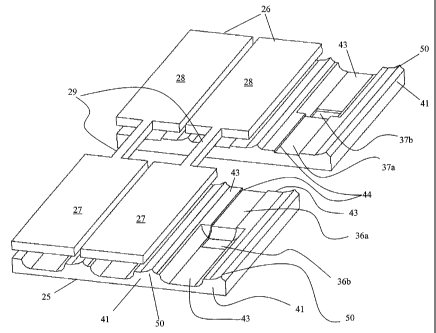
parallel to
each other. Unfortunately, this mirror construction restraint greatly
restricts other
design choices that have to be made in building the overall switch.
1
CA 02482165 2004-09-21
Doc. No. 10-602 CA Patent
[03] When using a conventional MEMs arrangement, the mirror 1
positioned on the planar surface 2 can be rotated through positive and
negative
angles, e.g. 2 , by attracting one side 10a or the other side 101) of the
planar
surface 2 to the substrate 6. Unfortunately, when the device is switched
between
ports at the extremes of the devices rotational path, the intermediate ports
receive light for fractions of a millisecond as the mirror 1 sweeps the
optical beam
past these ports, thereby causing undesirable optical transient or dynamic
cross-
talk.
[04] One solution to the problem of dynamic cross-talk is to initially or
simultaneously rotate the mirror about a second axis, thereby avoiding the
intermediate ports. An example of a MEMs mirror device pivotable about two
axes is illustrated in Figure 2, and includes a mirror platform 11 pivotally
mounted
by a first pair of torsion springs 12 and 13 to an external gimbal ring 14,
which is
in turn pivotally mounted to a substrate 16 by a second pair of torsion
springs 17
and 18. Examples of external gimbal devices are disclosed in United States
Patents Nos. 6,529,652 issued March 4, 2003 to Brenner, and 6,454,421 issued
September 24, 2002 to Yu et al. Unfortunately, an external gimbal ring greatly
limits the number of mirrors that can be arranged in a given area and the
relative
proximity thereof, i.e. the fill factor. Moreover, the external gimbal ring
may cause
unwanted reflections from light reflecting off the support frame. These
references
also require at least four electrodes to actuate each mirror.
[05] Another proposed solution to the problem uses high fill factor
mirrors,
such as the ones disclosed in United States Patent No. 6,533,947 issued March
18, 2003 to Nasiri et al, which include hinges hidden beneath the mirror
platform.
Unfortunately, these types of mirror devices require costly multi-step
fabrication
processes, which increase costs and result in low yields, and rely on four
different
pairs of electrodes for actuation.
[06] Another problem inherent with closely packed micro-mirrors is angular
drift caused by a build up of electrostatic charge on exposed dielectric or
insulating surfaces. The electric field generated by these electrostatic
charges
perturbs the electric field generated by the applied voltage from the
electrodes,
thereby causing the angular position of the platform to drift over time.
2
CA 02482165 2004-09-21
Doc. No. 10-602 CA Patent
[07] An object of the present invention is to overcome the shortcomings of
the prior art by providing a MEMs mirror device that has minimum angular drift
over time due to a raised or sunken ground electrode with a vertical gap
therebetween.
SUMMARY OF THE INVENTION
[08] Accordingly, the present invention relates to a micro-electro-
mechanical device mounted on a substrate comprising:
[09] a pivoting member pivotally mounted on said substrate about a first
axis;
[10] a first hot electrode beneath the pivoting member for pivoting the
pivoting member about the first axis;
[11] a first ground electrode beneath the second supporting region for
pivoting the pivoting member about the first axis;
[12] a first ground electrode adjacent to the first hot electrode separated
by
a substantially vertical step creating a gap between the first hot electrode
and the
first ground electrode; and
[13] a dielectric material in the gap for isolating the first hot electrode
from
the first ground electrode.
BRIEF DESCRIPTION OF THE DRAWINGS
[14] The invention will be described in greater detail with reference to
the
accompanying drawings which represent preferred embodiments thereof,
wherein:
[15] Figure 1 is an isometric view of a conventional tilting MEMs mirror
device;
[16] Figure 2 is a plan view of a pair of conventional external gimbal ring
MEMs mirror devices;
3
CA 02482165 2004-09-21
Doc. No. 10-602 CA Patent
[17] Figure 3 is an isometric view of a plurality of Piano-MEMs mirror
devices;
[18] Figure 4 is an isometric view of a hinge structure of the mirror
devices
of Fig. 3;
[19] Figure 5 is an isometric view of an electrode structure of the mirror
devices of Fig. 3;
[20] Figure 6 is an isometric view of a plurality of Piano-MEMs mirror
devices according to an alternative embodiment of the present invention with
electrode shields, light redirecting cusps, and a raised ground plane;
[21] Figure 7 is an isometric view of a plurality of Piano-MEMs mirror
devices according to an alternative embodiment of the present invention with
electrode shields;
[22] Figure 8 is a plan view of a pair of internal gimbal ring MEMs mirror
devices according to the present invention;
[23] Figure 9 is an isometric view of an internal gimbal ring MEMs mirror
device according to the present invention;
[24] Figure 10 is an isometric view of an alternative embodiment of the
internal gimbal ring MEMs mirror devices according to the present invention;
[25] Figure 11 is an isometric view of a hinge structure of the mirror
devices
of Fig. 9;
[26] Figure 12 is an isometric view of an electrode structure of the mirror
devices of Figs. 9 and 10;
[27] Figure 13 is a graph of Voltage vs Time provided by the electrode
structure of Fig. 11;
[28] Figure 14 is an isometric view of internal gimbal ring MEMs mirror
devices utilizing a three electrode arrangement according to the present
invention;
4
CA 02482165 2004-09-21
Doc. No. 10-602 CA Patent
[29] Figure 15 is an isometric view of the three electrode arrangement of
Figure 14;
[30] Figure 16 is a plan view of an ideal placement of the three electrodes
of Figures 14 and 15 relative to the pivoting platform;
[31] Figure 17 is a plan view of a possible misalignment of the three
electrodes of Figures 14 and 15;
[32] Figure 18 is a plan view of another possible misalignment of the three
electrodes of Figures 14 and 15;
[33] Figure 19 is a graph of Voltage vs Time for the three electrodes of
Figure 14 and 15;
[34] Figure 20 is an isometric view of another embodiment of the present
invention with an offset section on the pivoting member;
[35] Figure 21 is a plan view of the embodiment of Figure 20;
[36] Figure 22 is an end view of the embodiment of Figures 20 and 21;
[37] Figure 23 is a schematic diagram of a wavelength switch utilizing the
mirror devices of the present invention;
[38] Figure 24 is a schematic diagram of an input/output assembly for the
wavelength switch of Fig 23; and
[39] Figure 25 is a schematic diagram of an alternative embodiment of an
input assembly for the wavelength switch of Fig. 23.
DETAILED DESCRIPTION
[40] An array of "Piano" MEMs mirror devices 21, 22 and 23, which pivot
about a single axis of rotation Oy above a substrate 25, is illustrated in
Figures 3,
4 and 5. Each mirror device 21, 22 and 23 includes a pivoting member or
platform 26 defined by first and second substantially-rectangular planar
supporting regions 27 and 28 joined by a relatively-thin substantially-
rectangular
brace 29 extending therebetween. Typically, each planar surface is coated with
a
CA 02482165 2004-09-21
Doc. No. 10-602 CA Patent
reflective coating, e.g. gold, for simultaneously reflecting a pair of sub-
beams of
light traveling along parallel paths, as will be hereinafter discussed. Each
brace
29 acts like a lever and is pivotally mounted to anchor posts 30 and 31 via
first
and second torsional hinges 32 and 33, respectively. The anchor posts 30 and
31 extend upwardly from the substrate 25. The ends of the first torsional
hinge
32 are connected to the anchor post 30 and the brace 29 along the axis Oy.
Similarly, the ends of the second torsional hinge 32 are connected to the
anchor
post 31 and the brace 29 along the axis ey. Preferably, each of the first and
second torsional hinges 32 and 33 comprises a serpentine hinge, which are
considerably more robust than conventional torsional beam hinges. The
serpentine hinge is effectively longer than a normal torsional hinge, which
spans
the same distance, thereby providing greater deflection and strength, without
requiring the space that would be needed to extend a normal full-length
torsional
hinge.
[41] With particular reference to Figure 5, each platform 26 is rotated by
the
selective activation of a first electrode 36, which electro-statically
attracts the first
planar section 27 theretowards or by the selective activation of a second
electrode 37, which electro-statically attracts the second planar section 28
theretowards. A gap 38 is provided between the first and second electrodes 36
and 37 for receiving the anchor posts 31, which extend from the substrate 25
to
adjacent the platforms 26.
[42] In the disclosed open loop configuration, the angular position of the
platforms 26 depend non-linearly on the voltage applied by the electrodes 36
(or
37), i.e. as the applied voltage is i ncreased linearly, the incremental
change in
angular platform position is greater as the voltage increases. Accordingly,
there
is a maximum voltage, i.e. an angular platform position, at which the platform
angular position becomes unstable and will uncontrollably tilt until hitting
part of
the lower structure, e.g. the electrode 36. This maximum voltage sets the
range
of angular motion that the platform 26 can travel. The instability in the
platform's
angular position is a result of the distance between the platform 26 and the
electrode 36 (the hot electrode) decreasing more rapidly at the outer free
ends of
the platform 26 than at the inner sections, nearer the pivot axis Ely. As a
result,
6
CA 02482165 2004-09-21
Doc. No. 10-602 CA Patent
the force per unit length along the platform 26 increases more rapidly at the
outer
free ends of the platform 26 than the inner sections. To increase the
platform's
range of angular motion, the field strength, i.e. the force per unit area,
that is
sensed at the outer free ends of the platform 26 must be reduced. With
reference to Figures 5, this is accomplished by providing the electrodes 36
and
37 with a two-step configuration. Upper steps 36a and 37a are positioned
proximate the inner end of the platform 26, i.e. the Y axis, while lower steps
36b
and 37b are positioned under the outer free ends of the platform 26, thereby
making the gap between the platforms 26 and the electrodes 36 and 37 greater
at the outer free end than the inner end. The area of the lower steps 36b and
37b can also be made smaller, thereby reducing the force per unit area sensed
by the outer free end of the platform 26. Multi-step electrodes, e.g. three or
more
can also provide a more even distribution of force.
[43] A consequence of closely packed micro-mirrors is that the actuation of
a single mirror will impart a torque, i.e. an angular rotation, onto adjacent
mirrors
as a result of fringing electric fields. In an effort to minimize this cross-
talk,
electrode grounding shields 41 are positioned on the substrate 25 around or on
either side of the first and second electrodes 36 and 37 forming electrode
cavities, which are electrically isolated from each other. Figure 5
illustrates C-
shaped grounding shields 41, which include lateral portions 41a for partially
surrounding the first and second electrodes 36 and 37. The grounding shields
41
are kept at ground potential, i.e. the same as the mirrored platforms 26,
while one
of the first and second electrodes is held at an activation voltage, e.g. 100
Volts.
[44] Trace lines 36c and 37c electrically connect the electrodes 36 and 37,
respectively, to a voltage supply (not shown). Since the trace lines 36c and
37c
also act as a hot electrode, i.e. contributing to the total torque applied to
the
platform 26, covering the traces 36c and 37c with a ground plane 43 (Figure 6)
also reduces the force applied to the outer free end of the platform 26.
[45] Figure 6 also illustrates an alternative configuration for the electrode
36, in
which the two step hot electrode 36 is sunken slightly below a surrounding
grounded metallic surface, which is a continuation of the ground plane 43. A
small vertical step 44 between the hot electrode 36 and the surrounding ground
7
CA 02482165 2004-09-21
Doc. No. 10-602 CA Patent
plane 43 is a dielectric surface that isolates the hot electrode 36 from the
surrounding ground plane 43. This arrangement reduces the angular drift of the
platform 26, which is caused by a build up of electrostatic charges on exposed
dielectric or insulating surfaces. The electric field generated by these
electrostatic charges perturbs .the electric field generated by the applied
voltage
from the electrodes 36 and 37, thereby causing the angular position of the
platform 26 to drift over time. The present arrangement limits the exposed
dielectric to the small vertical surface 44, which generates electrostatic
field lines
that do not significantly affect the field lines between the hot electrodes 36
and 37
and the ground plane 43. To further reduce the angular drift of the platform
26,
the vertical surface 44 can be under cut beneath the ground plane 43 at a
slight
negative angle ensuring that the gap between the hot electrode 36 and the
ground plane 43 is substantially zero. The ground plane 43 could also be
positioned slightly below the hot electrodes 36 and 37 to create the vertical
step.
[46] Since the MEMs mirror devices 21, 22 and 23 are for use in optical
devices, i.e. wavelength blockers and multiple wavelength switches (see Figure
23), which include a grating for dispersing the light into spectral wavelength
component channels, it is an important performance requirement that the
spectral
response has a high rejection of light between the selected wavelength
channels.
Unfortunately, in conventional MEMs devices, light passes between the mirrors
and is reflected off the substrate back into the optical device, thereby
leading to a
deterioration in the isolation between the wavelength channels. Accordingly,
the
present invention provides back reflection cusps 50, defined by angled, curved
or
concave reflecting surfaces intersecting along a ridge, extending
longitudinally
below the gap between the platforms 26, for scattering any light passing
between
the mirrored platforms 26 in a direction substantially parallel to the surface
of the
platforms 26.
[47] To further eliminate cross-talk between adjacent electrodes,
additional
platform shields 42 (Figure 7) can be added to the underside of the planar
supporting regions 27 and 28, outside or inside of the electrode shields 41.
Typically, in the rest position, the two different sets of shields 41 and 42
do not
overlap; however, as the platform 26 tilts the platform shields 42 begin to
overlap
8
CA 02482165 2004-09-21
Doc. No. 10-602 CA Patent
the grounding shielding 41. The added protection provided by overlapping
shielding is particularly a dvantageous, when the tilt a ngle oft he platform
26 is
proportional to the voltage applied to the electrode 36 (or 37), such as in
open
loop configurations. Accordingly, the greater the tilt angle, the greater the
required voltage, and the greater the amount of potential cross-talk, but
consequently the greater the amount of shielding provided by the overlapping
ground and platform shields 41 and 42, respectively. Back reflection cusps 50
are also provided for reasons hereinbefore discussed. A single structure 50
between adjacent electrodes can replace the pair of adjacent shields 41.
[48] With reference to Figures 8, a pair of internal gimbal ring MEMs
mirror
devices 131 and 132 are illustrated mounted adjacent each other on a substrate
133. The present invention enables mirrors 134 and 135 to be positioned
relatively close together, i.e. with a high fill factor, while still providing
the two
degrees of motion provided by the more complicated prior art.
[49] With further reference to Figure 9, a first torsion hinge 137,
preferably
in the form of a rectangular beam, is fixed, proximate the middle thereof, to
the
substrate 133 via a central anchor post 138. The supporting structure for the
mirror device of the present invention is based on a single anchor post 138,
rather than the dual anchor points required in the aforementioned external
gimbal
ring devices. The first torsion hinge 137 provides for rotation Ay about a
first axis
Y, and may also include a serpentine hinge 140, as illustrated in mirror
device
131, or any other torsional hinge known in the art. Opposite sides of an
internal
gimbal ring 139 are connected to opposite ends of the first torsion hinge 137,
whereby the first torsion hinge 137 bisects the internal gimbal ring 139. The
internal gimbal ring 139 is preferably not flexible, but can take various
geometric
forms, although rectangular or circular frames would be the most convenient to
fabricate and use. Spring arms 141 and 142, which define a second torsion
hinge, extend outwardly from opposite sides of the internal gimbal ring 139
perpendicular to the first torsion hinge 137. Each of the spring arms may also
include a serpentine hinge as hereinbefore described. The second torsion hinge
provides for rotation 0õ about a second axis X, which is perpendicular to the
first
axis Y, but still substantially in the same plane as the mirrors 134 and 135.
A
9
CA 02482165 2004-09-21
Doc. No. 10-602 CA Patent
generally rectangular platform 143, for supporting one of the mirrors 134 or
135,
is mounted on the ends of the spring arms 141 and 142. Preferably, the
platform
143 is comprised of a pair of rectangular planar surfaces 144 and 145 joined
together by a pair of elongated braces 147 and 148, which extend on either
side
of the internal gimbal ring 139 parallel with the spring arms 141 and 142.
[50] Fabrication of the preferred embodiment illustrated in Figures 8 and
9,
is simplified by having all of the structural elements, i.e. the first
torsional hinge
137, the gimbal ring 139, the spring arms 141 and 142, and the first and
second
planar surfaces 144 and 145, in the same upper substrate layer and having
coplanar upper surfaces, whereby the same basic process steps are used as are
used to fabricate the MEMs device illustrated in Figure 1. In particular, a
single
photolithographic step is used to identify the structural elements, followed
by a
deep reactive ion etching (DRIE) step used to remove the unwanted portions of
the upper substrate. Finally the moveable elements in the upper substrate are
released from the lower substrate by removal of a sacrificial layer
therebetween.
[51] Figures 10 and 11 illustrate an array of internal gimbal ring MEMs
mirror devices 201 utilizing a first pair of serpentine torsional hinges 202
for
pivoting a rectangular platform 203, including first and second planar
supporting
regions 203a and 203b, about a first axis of rotation 6., and a second pair of
serpentine torsional hinges 204 for rotating the platform 203 about a second
axis
of rotation 6y above a base substrate 205. The first pair of serpentine
torsional
hinges 202 extend from a single anchor post 206, which extends upwardly from
the base substrate 205 through the center of the platform 203, i.e. at the
intersection of the minor and major axes thereof. Outer ends of the first pair
of
torsional serpentine torsional hinges 202 are connected to a rectangular
gimbal
ring 208, which surrounds the first pair of serpentine hinges 202, at points
along
the minor axes (6y) of the platform 203. The second pair of serpentine
torsional
hinges 204 extend from opposite sides of the gimbal ring 208 into contact with
the platform 203, at points along the major axis (60 of the platform 203.
[52] To provide a full range of motion for the platform 143 or 203, a set
of
four two-step electrodes 211, 212, 213 and 214 are provided (See Fig. 12);
however, for the present invention only the first, second and third electrodes
211,
CA 02482165 2004-09-21
Doc. No. 10-602 CA Patent
212 and 213 are required to roll the mirrors out of alignment with any
intermediate output ports and then back into alignment with a designated
output
port. As in Figure 5, each of the electrodes 211, 212, 213 and 214 include an
upper step 211a, 212a, 213a, and 214a, and a lower step 211b, 212b, 213b,
214b, respectively, for reasons discussed hereinbefore.
Accordingly, first,
second and third voltages can be established between the platform 143 or 203
and the first electrode 211, the second electrode 212 and the third electrode
213,
respectively. Initially, the first and second electrodes 211 and 212 are
activated
to rotate the platform 143 or 203 about O. S ubsequently, the first voltage is
gradually lowered to zero, while the third voltage is gradually increased
until it is
equivalent to the second voltage (See Fig 13). To minimize u nwanted effected
caused by ringing, i.e. vibration of the mirrors caused by an abrupt start or
stop,
the first, second and third voltages are increased and decreased gradually,
e.g.
exponentially, as evidenced in Figure 13, which illustrates the voltages
curves for
the various electrodes (first, second and third) over the actuation time of
the
mirror device. Various mirror tilting patterns can be designed based on the
desired characteristics, e.g. attenuation, of the light.
[53] An
improved electrode configuration is illustrated in Figures 14 and 15,
in which a first two-step ey electrode 236 includes an upper U-shaped step
236a,
and a lower rectangular step 236b. The arms of the U-shaped step 236a extend
from the lower step 236b on opposite sides of the second hinge 204 beneath the
first planar supporting region 203a. Similarly, a second two-step ey electrode
237
includes an upper U-shaped step 237a, and a lower rectangular step 237b. The
arms of the U-shaped step 237a extend from the lower rectangular step 237b on
opposite sides of the second hinge 204 beneath the second planar supporting
region 203b. A single two-step ex electrode 238 includes an upper U-shaped
step
238a, and lower rectangular steps 238b extending from each arm of the upper U-
shaped step. The single ex electrode 238 extends from adjacent the first ey
electrode 236 to adjacent the second ey electrode 237 across the gap
therebetween, and beneath one side of both the first and second planar
supporting regions 203a and 203b. The lower steps 238b provide a larger gap
between the outer free ends of the platform 203, when the platform is tilted
towards the first or the second ey electrode 236 or 237. The arms of the upper
U-
11
CA 02482165 2004-09-21
Doc. No. 10-602 CA Patent
shaped step 238b extend on opposite sides of the first pair of hinges 202. The
arms of the U-shaped step 238a are three to five times wider than the arms of
the
U-shaped step 236a or 237a. Multi-step electrodes are also possible to further
spread the application of force over the length of the platform 203. Actuation
of
the electrodes is controlled by an electrode control 240, as will be discussed
hereinafter with reference to Figure 19.
[54] An unfortunate consequence of relying on only three electrodes is that
a slight misalignment in positioning the platform 203 over the first and
second ey
electrodes 236 and 237 can result in an imbalance that can not be corrected
for
using the single ex electrode 238. Figure 16 illustrates the ideal case, in
which
the longitudinal axis of the first electrode 236 is aligned with the
longitudinal axis
X of the platform 203. However, Figure 17 illustrates the results of a mask
misalignment during fabrication, in which the longitudinal axis X of the
platform
203 has a +/ix misalignment relative to the electrode axis. Accordingly,
actuation
of the first ey electrode 236 would introduce an undesirable tilt in the
platform 203
towards the bottom left hand corner, which could not be compensated by the
single ex electrode 238. In Figure 18, the illustrated mask misalignment, in
which
the longitudinal axis X of the platform 203 has a--ax misalignment relative to
the
electrode axis. In this case, actuation of the first ey electrode 236 would
introduce an undesirable tilt in the platform 203 towards the top left hand
corner.
However, this tilt can be compensated for by applying a voltage to the single
ex
electrode 238. Accordingly, the solution to the problem of mask misalignment
is
to introduce an intentional or predetermined ¨Ax misalignment, which would
cancel or at least minimize any +Ax misalignment and which could be
compensated for by the single ex electrode 238.
[55] Figure 19 illustrates an electrode voltage vs time graph, detailing
the
voltages of the three electrodes 236, 237 and 238 as the platform 203 is
switched
from one position to another by an electrode control, i.e. from reflecting
light from
one port to another, without traveling directly, i.e. without reflecting light
into any
intermediate ports. To prevent undesirable "ringing" of the platform 203, the
voltage VyR of the first ey electrode 236 is gradually decreased as the
voltage Vx
of the single ex electrode 238 is increased. As the voltage V yR decreases to
12
CA 02482165 2004-09-21
Doc. No. 10-602 CA Patent
zero, the voltage VyL of the second ey electrode 237 gradually increases. As
the
voltage VyL reaches its set amount to maintain the platform in the desired
position, the voltage Vx is decreased to a minimum amount, assuming no
compensation voltages are required.
[56] When the size of t he p latform 203 is decreased, e.g. for small pitch
micro-mirrors in the order of <100um, the electrodes 236, 237 and 238 must
also
be constructed correspondingly smaller. However, due to the fact that the
electrodes necessarily become thinner, while sharing the same mirror section,
stable tilt angles are difficult to achieve at high resonant frequencies.
Accordingly, the size requirement of the electrode, and the required electrode
spacing become the limiting factor in determining the maximum fill factor. An
alternative embodiment of a three electrode configuration is illustrated in
Figures
20 and 21, in which platform 253 are made smaller than the original platforms
203 with first and second two-step ey electrodes 256 and 257 positioned
therebelow. A single ex electrode 258 is positioned below each offset section
259, which extends from the side of the platforms 253 adjacent the mid-section
thereof, i.e. the area of first and second hinges 251 and 252. This
arrangement
enables the single ex electrode 258 to be separated from the other two
electrodes
256 and 257, and therefore, be larger in size, which enables the electrostatic
torque to be increased for a common voltage. The added separation between
the electrodes 256, 257 and 258 minimizes the angular instabilities, when the
single ex electrode 238 is actuated, and reduces the amount of electrical x-
talk.
Preferably, the two-step ex electrodes 256 and 257 include the ground plane
arrangement as disclosed in Figure 6 with hot electrodes sunken relative to a
surrounding ground plane, and only a vertically extending dielectric layer,
which
provides a substantially zero-width vertical gap between the hot electrode and
the
ground plane.
[57] For high fill factor applications, a first planar section 253a of one
platform 253 is positioned beside a second planar section 253b of an adjacent
platform 253, as in Figures 20 and 21, whereby adjacent mirrors have offset x
axes Xi and X2, and every other platform pivots about the same x axis. Only
the
13
CA 02482165 2004-09-21
Doc. No. 10-602 CA Patent
relatively closely disposed planar sections would require reflective material
thereon, and reflective cusps 260 would only be required therebelow (Figure
22).
[58] Substrate-mounted, grounded cross-talk shields 261 and platform
mounted cross-talk shields 262 are provided to further minimize the amount of
electrical cross-talk between adjacent mirrors. The platform mount cross-talk
shields 262 are p referably m ounted outside oft he p latform mounted cross-
talk
shields 262 with enough spacing to enable rotation about both the x and the y
axis; however, any combination for offsetting the shields 261 and 262 is
possible.
[59] The "piano" M EMs mirror d evices according to the p resent i nvention
are particularly useful in a wavelength switch 301 illustrated in Figures 23,
24 and
25. In operation, a beam of light with a plurality of different wavelength
channels
is launched via an input/output assembly 302, which comprises a plurality of
input/output ports, e.g. first, second, third and fourth input/output ports
303, 304,
305 and 306, respectively. The beam is directed to an element having optical
power, such as concave mirror 309, which redirects the beam to a dispersive
element 311, e.g. a Bragg grating. The dispersive element separates the beam
into the distinct wavelength channels (A1, A2, A3) , which are again directed
to an
element having optical power, e.g. the concave mirror 309. The concave mirror
309 redirects the various wavelength channels to an array of "piano" MEMs
mirror devices 312 according to the present invention, which are independently
controlled to direct the various wavelength channels back to whichever
input/output port is desired. Wavelength channels designated for the same port
are reflected back off the concave mirror 309 to the dispersive element 311
for
recombination and redirection off the concave mirror 309 to the desired
input/output port. The concave mirror 309 can be replaced by a single lens
with
other elements of the switch on either side thereof or by a pair of lenses
with the
dispersive element 311 therebetween.
[60] With particular reference to Figure 24, the input/output assembly 302
includes a plurality of input/output fibers 313a to 313d with a corresponding
collimating lens 314a to 314d. A single lens 316 is used to convert a spatial
offset between the input/output ports into an angular offset. Figure 25
illustrates
a preferred embodiment of the input/output assembly, in which the unwanted
14
CA 02482165 2004-09-21
Doc. No. 10-602 CA Patent
effects of polarization diversity are eliminated by the use of a birefringent
crystal
317 and a waveplate 318. For incoming beams, the lens 316 directs each beam
through the birefringent crystal 317, which separates the beam into two
orthogonally polarized sub-beams (o and e). The half waveplate 318 is
positioned in the path of one of the sub-beams for rotating the polarization
thereof
by 90 , so that both of the sub-beams have the same polarization for
transmission into the remainder of the switch. Alternatively, the waveplate
318 is
a quarter waveplate and rotates one of the sub-beams by 45 in one direction,
while a nother q uarter waveplate 319 rotates the other sub-beam by 45 in the
opposite direction, whereby both sub-beams have the same polarization. For
outgoing light, the polarization of one (or both) of the similarly polarized
sub-
beams are rotated by the waveplate(s) 318 (and 319), so that the sub-beams
become orthogonally polarized. The orthogonally polarized sub-beams are then
recombined by the birefringent crystal 317 and output the appropriate
input/output port. The micro-electro-mechanical devices according to the
present
invention are particularly well suited for use in switching devices with
polarization
diversity front ends, since they provide a pair of reflecting surfaces, i.e.
one for
each sub-beam.