Note: Descriptions are shown in the official language in which they were submitted.
CA 02482350 2004-09-24
Electric Pulse Generator and ;Method for Generating Short Electric Pulses
BACKGROUND OF THE INVENTION
[0001] The invention relates to an electric pulse generator for generating
short
electric pulses as well as a method for generating short electric pulses.
[0002] Familiar electric pulse generators as well as methods for generating
short
electric pulses are generally based on the use of so-called step recovery
diodes (Sh'.D), the
rapid switch-off behavior of which is-exploited among other things to generate
short elec-
tric pulses. One disadvantage here is the difficult and relatively technically
complex
separation of the stimulating signal and the generated signal since a step
recovery diode is
a two-port element. Moreover the level of the selection signal must range in
the order of
~o magnitude of the desired output level since a passive step recovery diode
does not allow
signal amplification. Due to the few technical applications of step recover
diodes they
are additionally relatively difficult to procure and are accordingly
expensive.
SUMMARY OF THE INVENTION
is [0003] It is the object of the invention to provide an electric pulse
generator as
well as a method for generating short electric pulses, both being inexpensive,
reliable and
diverse in their use.
[0004) The electric pulse generator with which the above-described and pre-
sented object is achieved is characterized in that the following features are
provided: a
2o selection device to generate a control pulse, a transistor circuit or step
with a bipolar tran-
sistor to which the control pulse is fed and which subsequently emits an
output signal
with a steep switch-off side by exploiting the charge storage effect of the
bipolar transis-
tor, and a differentiation circuit or device, to which the output signal with
the steep
switch-off side is fed and which subsequently emits short primary pulses.
CA 02482350 2004-09-24
[0005] When using a fast, high frequency bipolar transistor for the transistor
de-
vice, short pulses having pulse widths clearly below 1 ns to below 90 ps can
be achieved
at amplitudes of a few volts. To be able to exploit the charge storage effect
of the bipolar
transistor the following should be noted:
[0006] The fast bipolar transistor, which is preferably operated in the common
emitter circuit, is initially directed by means of a suitable control signal
briefly into the
state of saturation so that both the base emitter diode and the base collector
diode become
conductive. The base collector space charge region, which is flooded this way
with mi-
nority carriers and is hence of low impedance; abruptly becomes high-impedance
after a
io brief period of delay when shutting off the transistor input signal, in the
present case the
control pulse leading to an abrupt increase in the collector voltage. In
relation to the tran-
sistor input signal generated by the selection circuit, the switch-off side of
the transistor
output signal is clearly steeper, wherein the polarity of the steeper switch-
off side de-
pends on the transistor type (NPN or PNP) that is used, the transistor base
circuit and the
is corresponding polarity of the control signal.
[0007] Apart from the emitter circuit, which is preferred in this case due to
the
high transistor current gain, for the bipolar transistor of the transistor
step also a collector
circuit or a base circuit of the bipolar transistor are possible.
[0008] The previously described electric pulse generator according to the
inven-
Zo tion is generally used to generate electric pulses with bipolar parts.
Frequently, however,
a pulse signal with purely monopolar parts is desired so that according to a
preferred em-
bodiment of the invention, a clipping device is provided which is arranged
downstream
from the differentiation step and to which is fed the short primary pulses,
wherein prede-
termined pulse portions are removed from the short primary pulses and a short
pulse sig-
ns nal is emitted. In particular, such a clipping device may be provided which
emits a mo-
nopolar short pulse signal.
[0009] For the design of the clipping device a variety of possibilities is
available.
Pursuant to preferred embodiments of the invention, it is, e.g., provided that
a Schottky
diode,
2
CA 02482350 2004-09-24
preferably having a low case capacitance, which is added serially into the
line, is used.
Moreover, transistors, preferably HF transistors, may be used in the clipping
device.
[0010] As control pulses, pulses having different pulse wave shapes may be
used.
Pursuant to a preferred embodiment of the invention, however; a pulse that
corresponds
substantially to a rectangular pulse and preferably has a pulse width in the
nanosecond
range is used as the control pulse.
[0011] In the differentiation device, in principle all known differentiation
tech-
niques may be applied. Pursuant to a preferred embodiment of the invention,
however, it
io is provided that the differentiation device has a planar circuit structure,
preferably in a
microstrip design. The function of the differentiation device here can be
expanded such
that in addition to the differentiation, a phase angle rotation and hence an
inversion of the
input signal takes place. To this end, in particular such a planar circuit
structure may be
provided that leads to polarity reversal.
is [0012) Pursuant to a preferred embodiment of the invention, alternatively
the dif
ferentiation device may comprise a transformer circuit. In particular, it may
be possible
to design the transformer circuit as being counterwound, thus causing a
polarity reversal.
[0013] It should be pointed out that in the transistor step especially also a
lzetero-
structure bipolar transistor may be used as the bipolar transistor.
Zo [0014) Finally, to further shorten the emitted pulse signal, it is provided
pursuant
to a preferred embodiment of the invention to include a plurality of
differentiation de-
vices, which are separated by a clipping device, respectively. Through this
preferred em-
bodiment of the invention, the pulse widths can be reduced even further;
however in this
case, a decrease in the amplitude must be tolerated.
is [0015] The method pursuant to the invention for generating short electric
pulses,
with which the above-described and presented object is achieved, is
characterized i.n that
a control pulse is generated, hat the control pulse is fed to a bipolar
transistor, which sub-
sequently emits an output signal with a steep switch-off side by exploiting
the aforemen-
tioned charge storage effect of the bipolar transistor, and that the output
signal with the
so steep switch-off side is differentiated so that short primary pulses are
generated.
3
CA 02482350 2004-09-24
[0016] Preferred embodiments of the method according to the invention are re-
vealed in analogy with the previously described embodiments of the electric
pulsf; gen-
erator according to the invention.
[0017] In detail, a variety of possibilities exist for designing and further
develop-
ing the inventive electric pulse generator as well as the inventive method for
generating
short electric pulses. To this end, reference shall be made to the dependent
patent claims
as well as to the following detailed description of preferred embodiments of
the invention
while referencing the drawings.
BRIEF DESCRIPTION OF THE DRAWINGS
io [0018] The drawings show:
Fig. 1 is a basic circuit diagram of an electric pulse generator that is based
on an
NPN bipolar transistor pursuant to a first preferred embodiment of the
invention;
Fig. 2 is a basic circuit diagram of a pulse generator that is based on a PNP
tran-
sistor pursuant to a second preferred embodiment of the invention;
is Figs. 3a to 3d are various planar implementation possibilities ofthe
differentiation
circuit or device pursuant to different preferred embodiments of the
invention;
Figs. 4a and 4b are various implementation possibilities of the
differentiation cir-
cuit or device pursuant to different preferred embodiments of the invention,
and
Fig. 5 is a basic circuit diagram for the use of a plurality of
differentiation circuits
Zo or devices that are separated by a clipping device, respectively, pursuant
to another pre-
ferred embodiment of the invention.
DESCRIPTIQN OF THE PREFERRED EMBODIMENTS
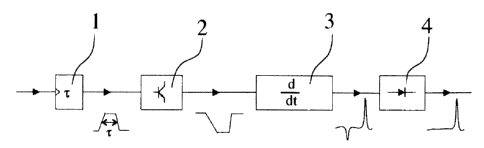
[0019] Fig. l shows a basic circuit diagram of a pulse generator pursuant to a
first preferred embodiment of the invention. The pulse generator comprises a
selection
Zs device 1 for generating a control pule, which corresponds substantially to
a rectangular
pulse having a pulse width i of several nanoseconds. This control pulse is fed
to a trap-
sistor circuit or device 2, which comprises an NPN bipolar transistor in the
emitter cir-
cuit. The transistor circuit or device 2 is followed by a differentiation
circuit or device 3,
which, in turn, is followed by a clipping device 4.
4
CA 02482350 2004-09-24
[0020] It was addressed already above that the rapid bipolar transistor that
is pro-
vided in the transistor circuit or device 2 in the form a three-port element
is beneficial in
that no further measures have to be taken for separating the input signal from
the output
signal, which significantly reduces the circuit complexity compared to pulse
generation
by means of a step recovery diode. Incidentally, it is true that apart from
the collector
circuit or base circuit of the bipolar ransistor, which are likewise possible
for the present
preferred embodiment of the invention, the emitter circuit is better suited
due to its tran-
sistor current gain.
[0021] To exploit the charge storage effect of the NPN bipolar transistor,
said
io transistor is first directed for a briefperiod into a state of saturation
so that both the base
emitter diode and the base collectordiode become conductive. Thus, the base
collector
space charge region is flooded with minority carriers and is hence of low
impedance.
When shutting off the transistor input signal, i.e. the control pulse coming
from the selec-
tion device 1, the existing base collector space charge region of low
impedance becomes
is abruptly high impedance again following a brief period of delay, leading to
a very rapid
increase in the collector voltage: In relation to the switch-off side of the
control pulse
entering the transistor, the switch-off side at the output of the transistor
or circuit device 2
is clearly steeper.
[0022] A comparison with Fig. 2, which illustrates a basic circuit diagram of
a
ao pulse generator with a PNP transistor that complements the pulse generator
described
here in the transistor circuit or device 2; reveals that the polarity of the
steeper switch-off
side depends on the transistor type (Nl'N or PNP) that is used. Incidentally,
the polarity
of the steeper switch-off side; as already indicated above, depends on the
transistor base
circuit that is used and the selection of the transistor.
is [4023] Pursuant to the preferred embodiments of the invention illustrated
in Figs.
1 and 2, the transistor circuit or device 2 is followed by a differentiation
circuit or device
3 and a clipping circuit or device 4, respectively, the functions of which are
as follows:
[0024] The differentiation circuit or device 3 is used to differentiate the
output
signal corning from the transistor circuit or device 2; said output signal
having a steep
3o switch=off side, so that the differentiatiorn circuit or device 3 must
primarily have hi:gh-
pass character. Figs: 3a to 3d show carious implementation possibilities of
the differen-
CA 02482350 2004-09-24
tiation circuit or device 3 having a rnicrostrip design according to preferred
embodiments
of the invention. Contrary to the networks 5 and 7 shown in Figs. 3a and 3c,
the net-
works 6 and 8 depicted in Figs. 3b and 3d, in addition to the differentiation,
cause a phase
angle rotation of the differentiated input signal by 180°, which
corresponds to polarity
reversal. The networks 6, 7 and 8 of Figs. 3b, 3c and 3d are line couplers
that have been
optimized for this purpose, which can be designed individually or as parallel
connections
of several line couplers (inter-digital coupler) depending on the desired
coupling. The
dimensions of the networks 5, 6, 7 and 8 with respect to line impedance, line
length and
the coupling of lines influence the resulting pulse width and pulse amplitude.
Since the
io design and function of the networks 5, 6, 7 and 8 shown in Figs. 3a through
3d are; evi-
dent to those skilled in the art without further explanations, a detailed
description is not
included here. It should only be pointed out that the networks 5, 6 and 8 have
planar
structures with lines that are partially short-circuited. against the signal
ground, while this
feature is not provided in network 7.
is [0025) Apart from the planar structures 5, 6, 7 and 8 shown in Figs. 3a to
3d also
transformer circuits 9 and 10 are suited as differentiation circuits or steps
3, as illustrated
in Figs. 4a and 4b, wherein a counterwound transformer circuit leads to
polarity reversal.
[0026) Moreover the differentiation circuit or devices 3 can be designed at
the
same time as directional couplers or as dupiexers for certain applications.
The two pulses
ao generated by the differentiation of the output signal coming from the
transistor device 2
exhibit apart from different polarity also different amplitudes, which can be
attributed to
the different gradients of the switch-on side and/or switch-off side of the
output signal of
the transistor circuit or device 2.
[0027) By means of the respective clipping device 4, e.g., an individual pulse
can
25 be extracted from the primary pulses emitted by the differentiation circuit
or devices 3.
Pursuant to a preferred embodiment of the invention, the clipping device 4 is
imple-
mented as a Schottky diode, which is added serially into the line, which clips
the cGrre-
sponding pulse in accordance with the selected polarity. When selecting the
Schottky
diode, attention should be paid, among other things, to a very low case
capacitance in or-
3o der to prevent capacitive cross-talk of the-clipped pulse. Also different
variations axe
suited as clipping devices 4, which are based on the fast HF transistors or
rapid HF-
6
CA 02482350 2004-09-24
suitable diodes and are inserted either serially or in parallel into the
output line of the dif
ferentiation circuit or device 3.
[0028) Finally, as illustrated in the preferred embodiment of the invention
shown
in Fig. 5, it is also provided to interlink several differentiation devices 3
and clipping de-
s vices 4, i.e. to provide a plurality of differentiation circuits or devices
3 separated by a
clipping device 4, respectively. Such interlinking of several differentiation
circuits or
devices 3 and clipping devices 4 leads to a decrease in the pulse width due to
multiple
differentiation of the pulse signal. Due to the clipping devices 4 which
generally have a
passive design, however, such a recurrent network also leads to a decrease in
the pulse
~o amplitude.
[0029) The pulses created witk the present invention are generally fed to <~
line,
such as a microstrip or a coaxial system with a defined characteristic
impedance. Ac-
cordingly, the output impedanceshould be adjusted to the characteristic
impedance of the
line. In relation to a 50 ohrn system; pulse widths of below 90 ps and
amplitudes of sev-
is eral volts can be achieved.
[0030) In relation to a voltage amplitude of, for example SV, a 50 ohm sy stem
re-
suits in a current of 100 mA and hence an instantaneous power of 500 mW.
Compared to
conventional pulse generation by means of step recovery diodes, which require
a control
signal that corresponds to the output power; the control power of the pulse
.generator de-
Zo scribed in the present invention is lower several times over so that it is,
e.g., possible to
control several pulse generators in parallel by means of a TTL signal.
What is claimed is: