Note: Descriptions are shown in the official language in which they were submitted.
CA 02482363 2010-05-17
TITLE OF THE INVENTION
THERMOELECTRIC DEVICE UTILIZING DOUBLE-SIDED PELTIER
JUNCTIONS AND METHOD OF MAKING THE DEVICE
BACKGROUND OF THE INVENTION
Field of the Invention
The present invention relates to a thermoelectric device having a plurality of
thermoelements arranged to improve the efficiency and the manufacturability of
the
thermoelectric device as compared to conventional thermoelectric device
arrangements.
Discussion of the Background
In U.S. Patent No. 6,300,150, a thermoelectric device and method for
manufacturing the same are disclosed, where a plurality of thermoelements
(p,n)
are disposed on the same side of a header, as shown in FIG. 6 of this patent.
The
surface of the interconnecting members is parallel to the header surface. A
cross-
section of this device is shown in FIG. 1.
The device includes a plurality of thermoelements that are disposed on the
same side of a cooling header. A p thermoelement 13 is connected on one side
by
metalization 12 to an electrical lead 11 on a first heat sink 10. The Peltier
junction
metalization (e.g. Cr/Au, Ni/Au, Cr/Au/Ni/Au), is electrically conductive. On
the
other side p thermoelement 13 is connected to a heat source (i.e., a header)
17 by
Peltier junction metalization 16. Element 14 is an ohmic metallization such as
Cr/Au
CA 02482363 2004-10-12
WO 2003/090286 PCT/US2003/011505
2
and element 15 is a diffusion barrier like Ni. An n thermoelement 19 is
connected on
one side by Peltier junction metalization 20 to electrical lead 21 on heat
sink 10. On
the other side n thermoelement 19 is connected to heat source 17 by Peltier
junction
metalization 16. Element 18 is an ohmic metallization like element 14. The
voltage
polarities (+,-) are shown for cooling.
There is one heat sink 10 common for both of the p and n thermoelements 13
and 19, and one heat-source (i.e., a header) 17 common to the thermoelements.
The n
and p elements are intermingled on the same side of header 17 during module
fabrication, which can complicate the manufacturing process.
SUMMARY OF THE INVENTION
One object of the present invention is to provide an improved thermoelectric
device.
Another object of the present invention is to simplify the manufacture of
thermoelectric device.
These and other objects are achieved by a thermoelectric device having a heat
source member, a first thermoelectric element of one conductivity type
connected to
one side of the heat source member, and a second thermoelectric element of a
conductivity type opposite to the one conductivity type connected to a side of
the heat
source member opposite to the one side.
A first heat sink may be attached to the first thermoelectric element, and a
second heat sink may be attached to the second thermoelectric element.
Contacts may be made to the first and second thermoelectric devices. The first
and second thermoelectric elements may be arranged so that a direction of
current
CA 02482363 2004-10-12
WO 2003/090286 PCT/US2003/011505
3
flow through the first and second thermoelectric elements is substantially the
same as
a direction of current flow through the contacts.
The first and second thermoelectric elements may each be a bulk element, a
thin film element, or a superlattice element.
The objects of the invention may also be achieved by a thermoelectric device
having a first thermoelectric element of a first conductivity type, a second
thermoelectric element of a conductivity type opposite to the first
conductivity type,
and a heat source member disposed between the first and second thermoelectric
elements.
Contacts may be formed to the first and second thermoelectric devices, and the
first and second thermoelectric elements and the contacts may be arranged so
that a
direction of current flow through the first and second thermoelectric elements
is
substantially the same as a direction of current flow through the contacts.
A first heat sink may be attached to the first thermoelectric element, and a
second heat sink may be attached to the second thermoelectric device.
The first and second thermoelectric elements may each be a bulk element, thin
film element, or a superlattice element.
The objects of the invention may also be achieved by a thermoelectric device
having a heat source member, a plurality of first thermoelectric elements of
only one
conductivity type connected to one side of the heat source member, and a
plurality of
second thermoelectric element of a conductivity type opposite to the one
conductivity
type connected to a side of the heat source member opposite to the one side.
A first heat sink may be attached to each of the plurality of first
thermoelectric
elements, and a second heat sink may be attached to each of the plurality of
second
thermoelectric elements.
CA 02482363 2004-10-12
WO 2003/090286 PCT/US2003/011505
4
The first and second thermoelectric elements and the contacts maybe arranged
so that a direction of current flow through respective pairs of the first and
second
thermoelectric elements is substantially the same as a direction of current
flow
through the contacts.
The first and second thermoelectric elements may each be a bulk element, a
thin film element, or a superlattice element.
The objects of the invention may further be achieved by a method of operating
a thermoelectric device having the step of arranging first and second
thermoelectric
elements on opposite sides of a heat source member such that only elements of
one
conductivity type are on each one of the sides. Contacts may be arranged
between
each of the elements and the member such that a current may be caused to flow
through respective pairs of the first and second thermoelectric elements in a
direction
substantially the same as a direction of current flow through the contacts.
BRIEF DESCRIPTION OF THE DRAWINGS
A more complete appreciation of the invention and many of the attendant
advantages thereof will be readily obtained as the same becomes better
understood by
reference to the following detailed description when considered in connection
with the
accompanying drawings, wherein:
FIG. 1 is a schematic diagram illustrating a conventional thermoelectric
device;
FIG. 2 is a schematic diagram illustrating a thermoelectric device according
to
the present invention;
FIG. 3 is a schematic diagram illustrating heat flow in the thermoelectric
device according to the present invention;
CA 02482363 2004-10-12
WO 2003/090286 PCT/US2003/011505
FIG. 4 is a schematic diagram of a thermally parallel, electrically series
thermoelectric module according to the present invention;
FIG. 5 is a schematic diagram of a thermally parallel, electrically series
thermoelectric module according to the present invention;
5 FIG. 6 is a schematic diagram of a thermally parallel, electrically parallel
thermoelectric module according to the present invention;
FIG. 7 is a schematic diagram illustrating dimensions of the thermoelectric
device according to the present invention;
FIG. 8 is a schematic diagram of a superlattice thermoelectric device
according
to the invention according to the present invention;
FIG. 9 is a cross-sectional diagram illustrating the manufacture of a
thermoelectric module according to the present invention;
FIG. 10 is a cross-sectional diagram illustrating the manufacture of a
thermoelectric module according to the present invention;
FIG. 11 is a cross-sectional diagram illustrating the manufacture of a
thermoelectric module according to the present invention;
FIG. 12 is a cross-sectional diagram illustrating the manufacture of a
thermoelectric module according to the present invention; and
FIG. 13 is a cross-sectional diagram illustrating the manufacture of a
thermoelectric module according to the present invention.
DESCRIPTION OF THE PREFERRED EMBODIMENTS
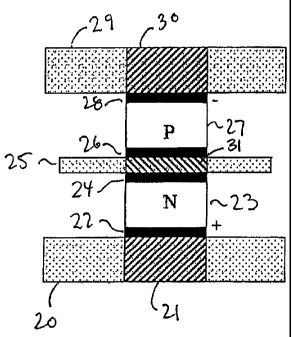
Referring now to the drawings, wherein like reference numerals designate
identical, or corresponding parts throughout the several views, and more
particularly
to Figure 2 thereof, Figure 2 is a first embodiment of the device according to
the
CA 02482363 2004-10-12
WO 2003/090286 PCT/US2003/011505
6
present invention. FIG. 2 illustrates a schematic diagram of The device where
the
voltage polarities (+,-) are shown for cooling. It is noted that the drawing
is not to
scale, but is drawn to illustrate the features of the device. Dimensions of
the elements
are discussed below, but the present invention is not limited to those
specific
dimensiona. The device includes a plurality of thermoelements disposed on
opposite
sides of a cooling header. A p thermoelement 27 is connected on one side by
Peltier
junction metalization 28 to an electrical lead 30 on a first heat sink 29. The
Peltier
junction metalization is electrically conductive. On the other side, p
thermoelement
27 is connected to a contact 31 on heat source (header) 25 by Peltier junction
metalization 26. An n thermoelement 23 is connected on one side by Peltier
junction
metalization 22 to electrical lead 21 on heat sink 20. The other side of n
thermoelement 23 is connected to contact 31 on heat source 25 by Peltier
junction
metalization 24.
N and p thermoelements are thin films of thickness in the range of microns to
tens of microns, grown or deposited or transferred on a substrate using
techniques
such as metallorganic chemical vapor deposition (MOCVD), chemical vapor
deposition (CVD), molecular beam epitaxy (MBE) and other epitaxial/non-
epitaxial
processes. The thin films can consist of thin-film superlattice or non-
superlattice
thermoelectric materials, quantum-well (two-dimensional quantum-confined) and
quantum-dot (three dimensional quantum-confined type) structured materials,
and
non-quantum-confined materials. Also, materials that are peeled from bulk
materials
can also be used.
The advantage of having p and n thermoelements 13 and 19 on opposite sides
of the header 17 is that it simplifies the arrangement of all p elements on
one side of
CA 02482363 2004-10-12
WO 2003/090286 PCT/US2003/011505
7
the heat source header and correspondingly the n elements on the opposite side
of the
heat source header.
The energy from heat source 25 is interfaced/communicated to the Peltier
junction. This can be achieved by flow of air or other high-thermal transfer-
coefficient liquids such as for example water or fluorocarbon fluids. This is
shown in
FIG. 3. Heat is absorbed (shown schematically by arrows 32) in parallel from,
for
example, the heat source fluids at the Peltier junction formed by
metalizations 24 and
26. The heat deposited in parallel on headers 20 and 29 is removed (shown
schematically by arrows 33 and 34, respectively). In this arrangement of FIG.
3, the
current flows from metal 28, through p thermoelement 27, through the Peltier
junctions, through n thermoelement 23 to metal 22. The p thermoelement 27 may
be
made of a p type material such as a Bi2Te3/Sb2Te3 superlattice or Si/Ge
superlattice
and the n thermoelement 23 may be made of an n type material such as a
Bi2Te3/Bi2Te3_,,Sex superlattice or a Si/Ge superlattice. Other suitable
superlattices of
thermoelectric materials having alternating lattice constants between the
individual
superlattice layers could be used, according to the present invention.
The arrangement according to the invention avoids the problem of
intermingling n and p elements on the same side of the header as discussed in
US Pat.
No. 6,300,150. This avoidance can lead to substantial advantages in assembly
of p
and n thermoelements, to produce a p-n couple and in turn a full-scale module.
This
can also lead to more convenient use of large-scale wafers as well. For
example, the
deposition of a similar type thermoelectric material, the patterning of the
deposited
thermoelectric materials, and subsequent metallization can occur on the same
thermoelectric device wafer. The device wafer, if of a suitable thermal
conductivity,
CA 02482363 2010-05-17
could compose the header itself. Otherwise, the deposited device layers could
be
removed from the device wafer and bonded on the header.
The thermoelements may be arranged in a number of configurations to form
modules. One example is shown in FIG. 4 where a thermally parallel,
electrically
series double-sided Peltier junction module is illustrated. Three
thermoelectric
devices 40, 41 and 42, with elements of the same conductivity type formed on
the
same side of the header, are connected to heat source 44 and heat sinks
(headers) 43
and 45. The movement of heat is schematically shown by the arrows. The (+, )
arrangement is shown for cooling.
Another example of a thermally parallel, electrically series double-sided
Peltier junction module is illustrated in FIG. 5. The module includes
thermoelectric
devices 50, 51 and 52 connected to heat source (header) 54 and heat sinks
(headers)
53 and 55. Heat transfer is shown by the arrows. Note the orientation of the n
and p
elements of the devices, relative to the headers, is alternated. Thus this
~"intermingled" configuration the n-element of device 50 is connected to is an
extension of the conventional p, non same side of header with the double side
Peltier
junction concept proposed in figure 4 p-element of device 51 by interconnect
56, and
the n-element of device 51 is connected to the p-element of device 52 by
interconnect
57. Here, the electrical leads 56 and 57 provide the electrical
interconnection between
adjacent devices. Note that these electrical leads or interconnects can be
routed
through compact coaxial electrical jigs at headers 53 and 55, if desired. The
electrical
routing is simpler than in the module of FIG. 4. Further, in some cases, these
electrical leads can be used as "radiators" of heat as long as the electrical
leads are on
the heat-sink side. See for example U.S. Patent No. 7,282,798.
8
CA 02482363 2004-10-12
WO 2003/090286 PCT/US2003/011505
9
One potential advantage of this thermally parallel, electrically series
thermoelectric module as shown in FIG. 5 compared to the single-side Peltier
junction, thermally parallel, electrically series thermoelectric module,
described in US
Pat. No. 6,300,150, is that the interconnect resistance at the Peltier
junction can be
significantly reduced. The reduction of interconnect resistance comes from the
fact
that, in this present invention, the current flowing through Peltier
metalization is along
the direction of current flow through the thermoelement. This can be
understood from
the fact that it is easier to reduce resistance in a vertical direction
compared to a lateral
direction.
A thermally parallel, electrically parallel, double-sided Peltier junction
module
is shown in FIG. 6. Devices 60, 61 and 62 are connected to heat sinks
(headers) 63
and 65 and heat source (header) 64. The heat flow is shown by the arrows. Each
of
the p-elements of devices 60-62 is connected to interconnect 66 and each of
the n-
elements of devices 60-62 is connected to interconnect 67. This arrangement
could be
useful especially for low- T (low cooling temperature requirements or low
heating
temperature requirement from ambient) systems as the current requirements are
lower.
Lower current requirements can be met with parallel confirmation of devices,
as here
however, the electrical routing is also significantly simpler compared to the
device of
FIG. 4.
Preferably, the p- and n-thermoelements are made of bulk or thin film
materials. The devices can be of any dimension to suit the application. FIG. 7
illustrates in general the dimensions of a thermoelement. In FIG. 7, a p-
thermoelement 70 is connected between contacts 71 and 72. For thin film
devices, 1
is in the range of approximately 1.0 m to 1000 gm, w is in the range of
approximately 10 gm to 1000 m, and h is in the range of approximately 1.0 gm
to
CA 02482363 2010-05-17
1000 gm. For bulk device, 1, h and w are each typically 1 mm. The elemental
dimensions for an n-thermoelement are expected to be similar to those for a p-
thermoelement, depending on the figure-of-merit (ZT), thermal conductivity (K)
and
other parameters such as Seebeck coefficient (cc) and electrical conductivity
((T) of
the n and p elements as described in Venkatasubramanian et al., Nature, vol.
413, pp.
597-602 (Oct 11, 2001),
Note circular cross sections and other cross-sections of thermoelements can
also be used although rectangular cross-sections as shown here.
Note the dimensions 1 and w of the thermoelements in Fig. 4-6, the depth of
the heat-source plate, and corresponding dimensions of the heat-sink plate can
be
designed to optimize the heat transfer coefficients. For example, the height
of Peltier
metalizations 71 and 72, as shown in FIG. 7, can be made different from the
height of
the heat-source plate, for better heat transfer (e.g. height of element 71 =
heights of
elements 28 and 30 combined, and the height of element 72 = heights of
elements 22
and 31 combined). For example, larger heights of the heat source plate can
lead to
easier fluid flow (though channels having a height of the Peltier metal in the
heat
source plate) while a smaller height of the Peltier metalization can lead to
lower
electrical resistance of Peltier metalization.
Another example of the n- and p-thermoelements according to the invention is
shown in FIG. 8. N-thermoelement 83 is a superlattice thermoelement
(schematically
shown by the parallel lines) is connected to electrical lead 81 of heat sink
(header) 80
by Peltier metalization 82 and to electrical lead 91 of heat source (header)
85 by
Peltier metalization 84. P-thermoelement 87 is a superlattice thermoelement
connected to electrical lead 90 of heat sink (header) 89 by Peltier
metalization 88 and
CA 02482363 2010-05-17
to electrical lead 91 of heat source (header) 85 by Peltier metalization 86.
Note that in
the superlattice n- and p-thermoelements, the current flow is perpendicular or
approximately perpendicular through the superlattice interfaces. The current
continues in the same direction through the Peltier junction metalization,
while going
from the p-thermoelement to the n-thermoelement. Superlattice thermoelements
may
be used in any arrangement, such as in FIGS. 4-6.
The device according to the invention is able to the lower the Peltier
junction
metalization resistance, and can achieve effective heat transfer between the
working
(heat-transfer) fluids and the Peltier junction metalization without
significant losses.
Effectively, the radiative and convective heat loses can be reduced with the
double-sided Peltier junction structure. The p and n thermoelements can also
be
quantum-confined structures or quantum-dot superlattice materials. These
materials
may also be arranged in numerous configurations such as shown in FIGS. 4-6.
The
thermoelectric device according to the invention may be used with thermal
spreaders/plates such as AIN, A1203, diamond, BeO, or other materials with
good
thermal conductivity. This device 'according to the invention can also be
combined
with cascading or multi-stage thermoelectric cooler concepts. See for example
U.S.
Patent No. 6,505,468,
Besides cooling, these devices may be applied for power conversion as well.
In FIGS. 1-8, heat will be absorbed in the heat-source plate, which is hotter
than the
heat-sink plate, and deposited at the heat-sink plate, thereby producing an
external
current. This is in contrast to the arrangement where an external power source
providing a current source to the cooler or heater when the thermoelectric
device is
operated in that mode.
- 11
CA 02482363 2004-10-12
WO 2003/090286 PCT/US2003/011505
12
These devices may be manufactured as shown in FIGS. 9-13. The
manufacturing techniques described in U.S. Patent No. 6,300,150 may be applied
and/or adapted for use in manufacturing the devices according to the
invention. In
FIG. 9, a cross-sectional view of a substrate 100 having thermoelectric
elements 101-
103 with corresponding Peltier metalizations 104-106 is shown. The
thermoelements
may be n- or p-type, and may be bulk, thin film or superlattice type elements.
The
thermoelements are formed using the techniques described typically as a layer
on
substrate 100. A layer of Peltier metalization may then be formed on the
layer. The
individual elements 101-103 are formed using standard patterning techniques,
such as
photolithography and etching to desired dimensions. The elements may be formed
in
any pattern, such as a matrix.
A heat sink (cooling header) 107 having a pattern of connections including
connections 108, 109 and 110 is attached to the elements through the Peltier
metalizations 104-106. The connections 108-110 and metalizations 104-106 form
electrical contacts having as low as possible resistance. The connections on
header
107 form a pattern to provide connections to and/or interconnect the
thermoelements
as desired. The substrate is then removed, as shown in FIG. 11, and a second
Peltier
metalization, forming metalizations 111, 112 and 113, is formed on the side of
thermoelements from which the substrate 100 was removed. Alternatively, at
least
some of the thermoelements may be directly deposited on the header 107. In a
preferred embodiment of the present invention, a substrate on which a
thermoelectric
material is deposited or which is being etched is maintained at a lower
temperature
than a precursor (e.g. a metal-organic) cracking temperature by deposition in
an
apparatus which includes a susceptor with separators, made of an optically
transmissive material with low thermal conductivity, such as quartz, upon
which the
CA 02482363 2004-10-12
WO 2003/090286 PCT/US2003/011505
13
substrates are mounted. The susceptor is heated to a precursor cracking
temperature
while the substrates are maintained at a lower deposition temperature by the
separators. The substrates are heated by black body radiation transmitted
through the
separators to the substrates. By methods such as those disclosed in the above-
noted
U.S. Pat. No. 6,071,351, the thermoelectric material can be deposited on a
header.
The header, according to the present invention, can include a semiconductor
wafer
itself, and by these low temperature techniques can be a processed
semiconductor
wafer containing integrated or power switching devices.
A heat source (header) 114 having connections 115, 116 and 117 is then
attached through the metalizations 111-113 to the thermoelements as shown in
FIG.
12. The connections in the header 114 are arranged in a desired pattern to
connect the
thermoelements 101-103 to thermoelements that are to be arranged on the other
side
of header 114.
Another set of thermoelements, having an opposite conductivity type to
thermoelements 101-13 are prepared in the same manner as described above in
FIGS.
9-11. As shown in FIG. 13, a second set of thermoelements 121, 122 and 123 are
attached to contacts 128, 129 and 130 of a heat sink (header) 127 through
Peltier
metalization 124, 125 and 126. The thermoelements 121-123 are attached to
connections 115-117 of header 114 through Peltier metalizations 118, 119 and
120.
Alternatively, at least some of the thermoelements and the Peltier
metallization may
be directly deposited on the header 127. Different patterns of connections in
the
headers can produce a series or parallel electrical connection of the
thermoelements.
Additionally, the present invention can utilize for the thermoelectric devices
a
transthermistor employing a unipolar p-p or n-n couple with two electrical
terminals
and three temperature terminals to achieve a very large temperature
differential across
CA 02482363 2010-05-17
each end of a unipolar couple, as described in U.S. Publication No.
2006/0225773
of October 12, 2006. For example, a p-p transthermistor unipolar couple can
be used in conjunction with an n-n transthermistor unipolar couple for ease of
integration into a modular device although a complete module can be
constructed with
a set of p-p or n-n unipolar transthermistor couples. The advantages of this
unipolar
transthermistor device include the use of only one type of polarity elements
like p-type
or n-type thermoelements, whichever has higher ZT. Current is driven in
opposite
directions through the pairs of unipolar elements to establish a temperature
differential
across each of the unipolar element pairs. For example, in the present
invention,
modules can be constructed using only p-type Bi2Te3/Sb2Te3 superlattice
thermoelements with a ZT of 2.5 at 300K, rather than combining with n-type
Bi2Te3-
based superlattice thermoelements with a ZT of -1.2 to 1.9 at 300K to form a
conventional p-n couple. Alternatively, the present invention can use only n-
type
PbTeSe/PbTe quantum-dot superlattice thermoelements with a ZT of -1.6 at 300K,
rather than combining with p-type PbTe-based superlattice thermoelements with
a
much lower ZT at 300K. In this approach, the thermoelement 27 depicted in
Figure 2
is constructed to be a n-type thermoelement, and current can be driven in
opposite
directs through tehrmoelements 27 and 23 to ensure cooling to the heat source
25.
Numerous applications are available for the double-sided Peltier junction
devices of the present invention. These applications include not only cooling
applications near room temperature (e.g., replacement of compression-based
cooling
engines in refrigerators and air conditioning units and other cooling devices,
replacement or augmentation of forced air cooling in semiconductor IC and
power
device thermal management, and replacement or augmentation of liquid phase
change
cooling, etc.) but extends to cryogenic cooling applications as well. For
example, one
14
CA 02482363 2004-10-12
WO 2003/090286 PCT/US2003/011505
application of the present invention is in the cooling superconducting coils
found in
electric motors and generators. In this case, thermoelectric devices of the
present
invention are placed in thermal contact with the superconducting coils.
Thermal
contact to the superconducting coils accomplished similar to those techniques
5 disclosed in U.S. Pat. No. 6,505,468. Large power industrial motors and
generators
can benefit significantly from the use of superconducting coils. The
application of
superconducting coils to industrial motors and generators would reduce
substantially
the rotor ohmic losses (i.e., I2R). The reduction in I2R loss would more than
compensate for the extra power required for refrigeration of the
superconducting coils.
10 While some high-temperature superconductors are superconducting at liquid
nitrogen
temperatures of 77 K, in the presence of magnetic fields (such as in electric
motors or
generators), the current carrying ability of these liquid nitrogen
superconductors is
deteriorated. Thus, more expensive liquid helium (at temperatures of 4.2 K) is
utilized to keep the superconducting coils at 30 to 50 K, where in the
presence of a
15 magnetic field the current carrying capability is not deteriorated.
More specifically, the double-sided Peltier junction devices of the present
invention could be utilized to in thermal contact with the backside of an
integrated
circuit chip or a power switching device as a cooling or power header. The
backside,
especially if it is electrically conducting, needs to be suitably modified to
confine the
electrical current to the thermoelectric element. One example of suitable
preparation
is p-n junction isolation in the backside of the chip whereby the current is
made to
flow through the intended thermoelectric electric elements, i.e. is confined
to the
elements, and is not shunted by the conducting backside of the chip. Other
modifications of the backside are possible to achieve similar confinement of
the
current. The backside then may be used to extract heat which could be used for
other
CA 02482363 2004-10-12
WO 2003/090286 PCT/US2003/011505
16
purposes such as power generation. For example, the power generated using the
heat
could be used provide power to other circuits or to other cooling devices.
Alternatively, the backside or the frontside of the integrated circuit chip or
a
semiconductor power switching device could be thermally connected to the
double-
sided Peltier junction devices of the present invention.
Numerous modifications and variations of the present invention are possible in
light of the above teachings. It is therefore to be understood that within the
scope of
the appended claims, the invention may be practiced otherwise than as
specifically
described herein.