Note: Descriptions are shown in the official language in which they were submitted.
CA 02482566 2004-10-13
WO 03/106693 PCT/US03/11721
GRADIENT STRUCTURES INTERFACING MICROFLUIDICS AND
NANOFLUIDICS, METHODS FOR FABRICATION AND USES THEREOF
This patent application claims the benefit of priority to U.S. Provisional
Patent
Application No. 60/373,407, filed on April 16, 2002 and U.S. Provisional
Patent
Application No. 60/419,742, filed October 18, 2002. DARPA Grant Number MDA972-
00-1-0031 supported work that led to portions of the inventions described
herein.
Accordingly, the U.S. Government may have rights in these inventions.
Background of the Invention
1. Field of the Invention
The present invention relates to bionanotechnology and in particular to a
method
of fabricating a hybrid microfluidic/nanofluidic device having a gradient
structure formed
by a modified photolithography technique at the interface between microfluidic
and
nanofluidic portions of the device and uses thereof.
2. Description of the Related Art
Nanotechnology, electronics and biology are combined in the newly emerging
field of bionanotechnology. Nanofabrication of extremely small fluidic
structures, such
as channels, can be used in bionanotechnology for the direct manipulation and
analysis of
biomolecules, such as DNA, and proteins at single molecule resolution. For
example, the
channels can be used for stretching genomic DNA and scanning for medically
relevant
genetic or epigenetic markers. New insights of understanding the confinement-
mediated
entropic behavior of biopolymers in ultra-small nanoscale fluidics have just
started to
emerge.
On the nanometer scale, DNA is a stiff molecule. The stiffness of the molecule
is
described by a parameter called the persistence length. Despite the relative
stiffness of
DNA for sufficiently long molecules, it tends to form a disordered tangle of
compact
random coils in free solution. The conformation of a polymer in free solution
has been
referred to as a spherical "blob" by the polymer dynamics community. The size
of the
blob depends on the length of the DNA molecule and the persistence length.
CA 02482566 2004-10-13
WO 03/106693 PCT/US03/11721
It has been described that in order to uniformly stretch chain-like long DNA,
dimensions of nanofluidic structures should be near, in the vicinity of or
smaller than the
persistence length of double stranded DNA of about 50 nm to about 70 nm.
Arrays of up
to half millions of nanochannels fabricated over a 100 mm wafer using
nanoimprinting
lithography (NIL) with sealed channels having a cross section as small as 10
nm by 50
nm to stretch, align and analyze long genomic DNA in a highly parallel
fashion, and the
resulting have been described in Cao H., Wang J., Tegenfeldt P., Austin R.H.,
Chen E.,
Wei W. and Chou S.Y., Fabrication of l Onm Enclosed Nanofluidic Channels
(2002)
Applied Physics Letters, Vol. 81, No. 1, pp174. It is challenging to
efficiently move long
DNA arranged as a blob into the small channels, since it is energetically
unfavorable for
long biopolymers to spontaneously elongate and enter nanochannels directly
from the
environment due to the large free energy needed to overcome negative entropy
change, as
illustrated in Figs. lA - 1B. For example, a double stranded T4 phage DNA
molecule
with a length of 169 kilobases will form a Gaussian coil with a radius of
gyration
Rg=(Lp/6)I~2 , where L is the length and p the persistence length of the DNA),
approximately 700 nm in aqueous buffer solution which is many times the width
of the
opening of the nanochannels. Consequently, problems such as DNA clogging at
the
junction of nano- and macro-environment have arisen and undermine the
performance of
conventional nanofluidic devices.
U.S. Patent Application No. 2002/0160365 describes a method for separation of
long strands of DNA by length by forcing the molecules to traverse a boundary
between a
low-force energy region and a high-force energy region. The high-force energy
region is
a diverse pillar region. The low-force energy region is a larger chamber
formed adjacent
the high-force energy region.
U.S. Patent Application No. 2002/0072243 describes fabrication techniques
using
a pattern of sacrificial and permanent layers to define the interior geometry
of a fluidic
device. A pattern for a fluidic device having microchannels and an array of
retarding
obstacles is defined in a resist layer. The pattern is produced using
lithographic
techniques. For electron beam lithography and for deep structures made with
photolithography, a hard pattern mask is required to assist in pattern
transfer. An inlet
chamber, outlet chamber, inlet microchannel, outlet chamber and an array of
holes is
2
CA 02482566 2004-10-13
WO 03/106693 PCT/US03/11721
formed in a sacrificial layer. A ceiling layer is deposited to cover the
sacrificial layer.
The ceiling layer enters the holes to form closely spaced pillars. The
sacrificial layer is
removed to form microchannels between the floor and ceiling layers. The
pillars act as a
sieve or an artificial gel filter for fluid flowing through the system. Steps
needed in
removing the sacrificial materials, such as heating the substrate up to 200 -
400° C, limits
the use of certain materials. Electron beam lithography has the flexibility to
write
different patterns, but has low throughput and high manufacturing costs.
It is desirable to provide an improved structure interfacing between
microfluidic
and nanofluidic components of a device for reducing the local entropic barrier
to
nanochannel entry and an improved method for fabrication thereof.
Summary of the Invention
The present invention relates to a device for interfacing nanofluidic and
microfluidic components suitable for use in performing high throughput i.e.,
macromolecular analysis. Diffraction gradient lithography (DGL) is used to
form a
gradient interface between a microfluidic area and a nanofluidic area. The
gradient
interface area reduces the local entropic barrier to nanochannels formed in
the nanofluidic
area.
In one embodiment, the gradient interface area is formed of lateral spatial
gradient
structures for narrowing the cross section of a value from the micron to the
nanometer
length scale. In another embodiment, the gradient interface area is formed of
a vertical
sloped gradient structure. Additionally, the gradient structure can provide
both a lateral
and vertical gradient. The gradient structures can be used to squeeze and
funnel
biomolecules into a small nanofluidic area.
In one aspect of the invention, a method for fabricating a fluidic device by
diffraction gradient lithography comprises forming a nanofluidic area on a
substrate,
forming a microfluidic area on the substrate and forming a gradient interface
area
between the nanofluidic area and the microfluidic area. The gradient interface
area can
be formed by using a blocking mask positioned above a photo mask and/or
photoresist
during photolithography. The edge of the blocking mask provides diffraction to
cast a
3
CA 02482566 2004-10-13
WO 03/106693 PCT/US03/11721
gradient light intensity on the photoresist. In another embodiment, a system
is provided
for fabricating the fluidic device.
In one aspect of the invention, the nanofluidic components comprise nanoscale
fluidic structures. The nanofluidic structures can include nanopillars,
nanopores and
nanochannel arrays.
In another aspect of the invention, a fluidic device is formed of a gradient
interface between a nanofluidic area and a microfluidic area, at least one
sample reservoir
in fluid communication with the microfluidic area, the sample reservoir
capable of
releasing a fluid and at least one waste reservoir in fluid communication with
the
nanofluidic area, the waste reservoir capable of receiving a fluid. In another
aspect a
system for carrying out analysis is provided including a fluidic device is
formed of a
gradient interface between a nanofluidic area and a microfluidic area, at
least one sample
reservoir in fluid communication with the microfluidic area, the sample at
least one
reservoir capable of releasing a fluid and at least one waste reservoir in
fluid
communication with at least one of the channels the waste reservoir capable of
receiving
a fluid, signal acquisition and a data processor. The signal can be a photon,
electrical
current/impedance measurement or change in measurements. The fluidic device
can be
used in MEMS and NEMS devices.
In another embodiment, methods for analyzing at least one macromolecule are
provided which, for example, include the steps of: providing a fluidic device
formed of a
gradient interface between a nanofluidic area and a microfluidic area, at
least one sample
reservoir in fluid communication with the microfluidic area, the at least one
sample
reservoir capable of releasing a fluid and at least one waste reservoir in
fluid
communication with the nanofluidic area, the waste reservoir capable of
receiving a fluid,
transporting at least one macromolecule from the microfluidic area to the
nanofluidic area
to elongate the at least one macromolecule, detecting at least one signal
transmitted from
the at least one macromolecule and correlating the detected signal to at least
one property
of the macromolecule.
Cartridges including a nanofluidic chip in accordance with this invention are
also
disclosed herein. Such cartridges are capable of being inserted into, used
with and
removed from a system such as those shown herein. Cartridges useful with
analytical
4
CA 02482566 2004-10-13
WO 03/106693 PCT/US03/11721
systems other than the systems of the present invention are also comprehended
by this
invention.
The invention will be more fully described by reference to the following
drawings.
Brief Description of the Drawings
Fig. lA is a schematic diagram of a prior art device including nanochannels.
Fig. 1B is a graph of entropy change to the nanochannels of the device of Fig.
lA.
Fig. 2 is a schematic diagram of a device for interfacing microfluidic and
nanofluidic components in accordance with the teachings of the present
invention.
Fig. 3 is a graph of entropy change to the nanochannels of the device of Fig.
2.
Figs. 4A - 4D diagrammatically illustrate a process incorporating diffraction
gradient lithography (DGL) to fabricate a micropost array and interface
gradient
structure.
Figs. SA-SB diagrammatically illustrate a process incorporating diffraction
gradient lithography (DGL) to fabricate a sloped gradient interface area.
Fig. 6A is a schematic diagram of a method for adjusting the diffraction
gradient
using thickness.
Fig. 6B is a schematic diagram of a method for adjusting the diffraction
gradient
using a variable distance.
Fig. 7 is a schematic diagram of a microfluidic/nanofluidic chip.
Fig. 8 is a schematic diagram of a system for analyzing macromolecules using
the
microfluidic/nanofluidic chip.
Fig. 9A is an optical image during fabrication of the device of the present
invention after photoresist development, in accordance with Fig. 4B, step 4.
Fig. 9B is a scanning electronic microscope during fabrication of the device
of the
present invention after pattern transfer and photoresist removal, in
accordance with Fig.
4C, step 5.
Fig. l0A is a scanning electronic microscope during fabrication of the device
of
the present invention after pattern transfer and photoresist removal using a
first etching
condition, in accordance with Fig. 4C, step 5.
5
CA 02482566 2004-10-13
WO 03/106693 PCT/US03/11721
Fig. l OB is a scanning electronic microscope during fabrication of the device
of
the present invention after pattern transfer and photoresist removal using a
second etching
condition, in accordance with Fig. 4C, step 5.
Fig. 11A is an intensified charge coupled device (CCD) image of fluorescent
long
DNA molecules entering the prior art nanofluidic chip shown in Fig. 1.
Fig. 11B is an intensified charge coupled device (CCD) image of fluorescent
long
DNA molecules entering device 10 shown in Fig. 2.
Detailed Description
Reference will now be made in greater detail to a preferred embodiment of the
invention, an example of which is illustrated in the accompanying drawings.
Wherever
possible, the same reference numerals will be used throughout the drawings and
the
description to refer to the same or like parts.
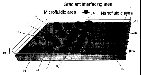
Fig. 2 is a schematic diagram of device 10 for interfacing microfluidic and
nanofluidic components in accordance with the teachings of the present
invention.
Gradient interface area 12 is positioned between microfluidic area 14 and
nanofluidic
area 16. Microfluidic area 14 can comprise a plurality of microposts 18 formed
on
substrate 19. For example, microposts 18 can have a diameter in the range of
about 0.5 to
about 5.0 microns and distance D~ between microposts 18 can be in the range of
about
0.5 to about 5.0 microns. In one embodiment, microposts 18 have a diameter in
the range
of about 1.2 to about 1.4 microns and a distance D1 between microposts 18 in a
range of
about 1.5 to about 2.0 microns.
Nanofluidic area 16 can comprise a plurality of nanochannel arrays 20
including a
surface having a plurality of nanochannels 21 in the material of the surface.
By "a
plurality of channels" is meant more than two channels, typically more than 5,
and even
typically more than 10, 96, 100, 384, 1,000, 1,536, 10,000, 100,000 and
1,000,000
channels. Nanochannels 21 can be provided as a plurality of parallel linear
channels
across substrate 19. Nanochannels 21 can have a trench width of less than
about 1 SO
nanometers, more typically less than 100 nanometers, and even more typically
less than:
75, 50, 25 and 15 nanometers. In certain embodiments, the trench width can be
about 10
nanometers. In the present invention, the trench width can be at least 2 nm,
and typically
6
CA 02482566 2004-10-13
WO 03/106693 PCT/US03/11721
at least 5 nm. Nanochannels 21 can have a trench depth of less than about 200
nanometers.
The nanochannels can have sealing material adjacent to the channel wall
material.
In this embodiment, the sealing material can reduce the trench width. Varying
the sealing
material deposition parameters can be used to narrow the trench width of the
channels.
The deposition parameters can be varied to provide trench widths of typically
less than
100 nanometers. As more material is deposited, trench widths can be narrowed
to less
than 75 nanometers, and even less than: 50 nanometers, 25 nanometers, and 15
nanometers. Trench widths of about 10 nm can also be provided by the methods
of the
present invention. Typically, the resulting trench widths after deposition
will be greater
than 2 nm, and more typically greater than 5 nanometers. Trench depths of less
than 175,
150, 125, 100, 75, 50, and 25 nm can also be provided by the methods of the
present
invention. Trench depths of about 15 nm can also be provided. Typically, the
trench
depths will be at least 5 nm, and more typically at least 10 nm.
In certain embodiments, the trench depth is typically less than 175 nm, and
more
typically less than 150 nm, 125 nm, 100 nm, 75 nm, 50 nm and 25 nm. In certain
embodiments, the trench depth is about 15 nm. In certain embodiments, the
trench depth
is at least 2 nm, typically at least 5 nm, and more typically at least 10 nm.
At least some
of the nanochannels 21 can be surmounted by sealing material to render such
channels at
least substantially enclosed. The lengths of the channels of the nanochannel
array can
have a wide range.
The lengths of the channels can also be the same or different in nanochannel
array
20. For carrying out macromolecular analysis using nanochannel array 20 as
provided
below, it is desirable that nanochannels 21 are at least about 1 millimeter
(mm), 1
micrometer (gym) or longer. The length of nanochannels 21 is greater than
about 1
millimeter (mm), about 1 centimeter (cm), and even greater than about 5 cm,
about 15
cm, and about 25 cm. Nanochannels 21 can be fabricated with
nanoimprint~lithography
(NIL), as described in Z. N. Yu, P. Deshpande, W. Wu, J. Wang and S. Y. Chou,
Appl.
Phys. Lett. 77 (7), 927 (2000); S.Y. Chou, P.R. Krauss, and P.J. Renstrom,
Appl. Phys.
Lett. 67 (21), 3114 (1995); Stephen Y. Chou, Peter R. Krauss and Preston J.
Renstrom,
Science 272, 85 (1996) and U.S. Patent No. 5,772,905 hereby each incorporated
in their
7
CA 02482566 2004-10-13
WO 03/106693 PCT/US03/11721
entirety by reference into this application. Nanochannel 21 can be formed by
nanoimprint lithography, interference lithography, self assembled copolymer
pattern
transfer, spin coating, electron beam lithography, focused ion beam milling,
photolithography, reactive ion-etching, wet-etching, plasma-enhanced chemical
vapor
deposition, electron beam evaporation, sputter deposition, and combinations
thereof.
Alternatively, other conventional methods can be used to form nanochannels.
In an alternate embodiment, nanofluidic area 16 can comprise nanoscale fluidic
structures. For example, the nanoscale fluidic structures can comprise
nanopillars and
nanospheres.
Gradient interface area 12 is used to effectively stretch and align
biopolymers 22
before they approach nanofluidic area 16. Biopolymers 22 can be preliminarily
stretched
between adjacent pairs of microposts 18 before entering nanochannels 21.
Gradient
interface area 12 reduces the steepness of the entrophy barrier before
biopolymers 22
enter nanofluidic area 16, as shown in Fig. 3.
Referring to Fig. 2, gradient interface area 12 can comprise a plurality of
gradient
structures 23 formed on substrate 19. Distance D2 between gradient structures
23 is
gradually reduced towards nanofluidic area 16. For example, distance D2
between
gradient structures 23 can be reduced from about 2 microns to gradually below
about 500
nm, about 400 nm, about 200 nm, about 150 nm, about 10 nm, about 5 nm and
about 2
nm. In one embodiment, the distance DZ between gradient structures 23 is
reduced in a
range of about a radius of gyration of biopolymer 22 to substantially a
diameter of
biopolymer 22. For example, diameter D2 between gradient structures 23 can be
reduced
in the range of about 2 nm, a diameter of a DNA module, to about 700 nm, a
radius of
gyration of a T4 phage DNA molecule.
Gradient structures 23 can provide a gradual elevation of height H~ from
substrate
19. Nanofluidic area 16 can have a shallower depth DP1 than depth DPZ of
microfluidic
area 14. Accordingly, gradual elevation of height H, from microfluidic area 14
to
nanofluidic area 16 provides improved interconnection of microfluidic area 14
with
nanofluidic area 16.
Basic fabrication steps of the present invention using diffraction gradient
lithography are outlined in partial, schematic perspective views in Figs. 4A -
4C, as
CA 02482566 2004-10-13
WO 03/106693 PCT/US03/11721
including processing steps 1-3. One or more nanochannels 21 were fabricated on
substrate 19 in this process. Substrate 19 can be a silicon wafer substrate.
Alternatively,
any type of material compatible with the photolithography can be used as a
substrate.
Substrate 19 was coated with photoresist 32 after HMDS treatment and baked.
Photomask 34 having a micron size post array can be used to pattern
microfluidic area 14
and gradient interface area 12, in step 1.
In step 2, blocking mask 35 was placed over or coated on photomask 34.
Blocking mask 35 extends over portion 36 of photomask 34. Blocking mask 35
masks
portion 38 of nanofluidic area 16 positioned under portion 36 of photomask 34
to protect
nanochannels 21. In step 3, device 10 was exposed to incident LTV light 37.
Blocking
mask 35 causes light diffraction along edge 39 of blocking mask 35.
Blocking mask 35 can be formed of any material which is opaque to exposing
light used in optical lithography. For example, blocking mask 35 can be formed
of a
metal, such as aluminum foil or an opaque plastic.
Referring to Fig. 4B, in step 4, device 10 was developed using conventional
techniques. Light diffraction caused by edge 39 of blocking mask 35 generates
a gradient
in dissolution rate of photoresist 32 by the developer. During development,
exposed
photoresist 32 was completely removed at portion 41 which is not blocked by
blocking
mask 35, exposing the substrate surface underneath. At portion 42, photoresist
32 has a
gradient of undeveloped photoresist along the light diffraction area. The
thickness of the
gradient of undeveloped photoresist corresponds to exposure to diffracted
light. At
portion 43, blocking mask 35 completely blocks exposure of photoresist 32 to
light.
Referring to Fig. 4C, in step 5, photoresist 32 was used as an etching mask
during
a reactive ion etching (RIE) process and gradient patterns in photoresist 32
were
transferred into substrate 19.
A light intensity profile on photomask 34 is shown in Fig. 4D. The light
intensity
profile shows reduced light intensity along edge 39 of blocking mask 35. The
gradient
profile can be controlled by the type of photoresist, development conditions
and etching
conditions. For example, a low contrast resist can provide a gradual gradient
profile.
Edge 39 of blocking mask 35 can be varied to adjust the gradient profile. For
example,
edge 39 can be angled or patterned to adjust the gradient profile.
9
CA 02482566 2004-10-13
WO 03/106693 PCT/US03/11721
In one embodiment, gradient interface area 12 is formed as a gradual slope
from
microfluidic area 14 to nanofluidic area 16, as shown in Figs. SA-SB. In this
embodiment, one or more nanochannels were fabricated in substrate 19.
Substrate 19
was coated with photoresist 32 after HMDS treatment and baked, in step 1. In
step 2,
S blocking mask 35 was placed over photoresist 32. Blocking mask 35 extends
over
portion 36 of photomask 34. Blocking mask 35 masks portion 38 of nanofluidic
area 16
to protect nanochannels 21. In step 3, device 10 was exposed to incident UV
light 37.
Blocking mask 35 causes light diffraction along edge 39 of blocking mask 35.
In step 4,
device 10 was developed using conventional techniques. Photoresist 32 was used
as an
etching mask during a reactive ion etching (RIE) process and gradient patterns
in
photoresist 32 were transferred into substrate 19. During development, the
diminishing
light intensity casted on photoresist 32 forms a gradient vertical slope in
gradient
interface area 12 which is transferred into substrate 16.
Width W2 of blocking mask 35 and distance between photomask 34 and blocking
mask 35 can be varied to determine the distance D3 of blocking mask 35 to
photoresist
32, as shown in Figs. 6A-6B. For example, blocking mask 35 can have a varying
width
W2 in the range of about 1 mm to about 10 mm. WZ can be formed of one or more
additional blocking masks which are fused to blocking mask 35 for increasing
Width WZ
of blocking mask 35. Blocking mask 35 can be coated on photomask 34.
In an alternate embodiment, distance D3 of blocking mask 35 to photoresist 32
can be adjusted by adjusting the distance between blocking mask 35 and
photomask 34.
Blocking mask 35 can be positioned over photomask 34 using blocking mask
holder 40.
Photomask 34 can be positioned over photoresist 32 using aligner 42. Blocking
mask
holder 40 can move blocking mask in X1, XZ, Yi, YZ directions. Aligner.42 can
move
photomask 34 in the X1, X2, Y1, Y2 directions. Distance D3 can be varied upon
movement of blocking mask 35 towards and away from photoresist 32. Distance D3
determines diffraction to photoresist 32. For example, a smaller distance D3
provides a
narrower diffraction zone in gradient interface area 12.
In another aspect of the invention, there is provided a
microfluidic/nanofluidic
chip that includes the gradient interface area for interfacing microfluidic
and nanofluidic
components. Referring to Fig. 7, microfluidic/nanofluidic chip 100 has
microfluidic area
CA 02482566 2004-10-13
WO 03/106693 PCT/US03/11721
14, substrate 19, nanofluidic area 16, gradient interface area 12 and
reservoirs 102 for
handling samples and reservoirs 104 for receiving samples and sample
collection.
Tunnels 103 formed in substrate 19 can be used for connecting reservoirs 102
and 104
respectively to microfluidic area 14 and nanofluidic area 16.
Nanofluidic area 16 can comprise nanofluidic channels 21 as described above.
Alternatively, nanofluidic area 16 and gradient interface area 12 can comprise
branched
channels 106. Branched channels 106 can be split into smaller and smaller
branches
range from about 5.0 microns to about 2 nanometers to provide decreasing
lateral
gradient distances between channels providing a lateral gradient. Branched
channels 106
can include a gradual elevation in height formed using diffraction gradient
lithography, as
described above.
The reservoirs are in fluid communication with at least one of the channels,
so
that the sample reservoirs are capable of releasing a fluid into the channels,
and the waste
reservoirs are capable of receiving a fluid from the channels. Typically the
fluids contain
macromolecules for analysis.
In certain embodiments of the present invention, the microfluidic/nanofluidic
chip
contains at least one sample reservoir formed in the surface of the substrate.
Reservoirs
can be defined using photolithography and subsequently pattern transferred to
the
substrate using Reactive Ion etching (RIE), chemical etching or FIB milling
directly to
create reservoirs in fluid communication with nanofluidic area 16 or
nanochannels 21. In
this embodiment, at least one waste reservoir in fluid communication with at
least one of
the channels. Typically, the microfluidic/nanofluidic chip contains at least 1
sample
reservoir. Alternatively, a variety of other embodiments include various
numbers of
reservoirs.
For use in macromolecular analysis, microfluidic/nanofluidic chip 100 can
provide at least a portion of nanofluidic area 16 capable of being imaged with
a two-
dimensional detector. Imaging of the nanofluidic area 16 is provided by
presenting the
nanochannels and any sealing material to suitable apparatus for the collection
of emitted
signals, such as optical elements for the collection of light from the
nanochannels. In this
embodiment, the microfluidic/nanofluidic chip is capable of transporting a
plurality of
11
CA 02482566 2004-10-13
WO 03/106693 PCT/US03/11721
elongated macromolecules from a sample reservoir, across macrofluidic area and
across
the nanofluidic area.
In certain embodiments of the present invention, the microfluidic/nanofluidic
chip
contains an apparatus for transporting macromolecules from the sample
reservoirs,
through the macrofluidic area, nanofluidic area, and into the waste
reservoirs. A suitable
apparatus includes at least one pair of electrodes capable of applying an
electric field
across at least some of the channels in at least one direction. Electrode
metal contacts can
be integrated using standard integrated circuit fabrication technology to be
in contact with
at least one sample and at least one collection/waste reservoir to establish
directional
electric field. Alternating current (AC), direct current (DC), or both types
of fields can be
applied. The electrodes can be made of almost any metal, and are typically
thin A1 /Au
metal layers deposited on defined line paths. Typically at least one end of
one electrode
is in contact with buffer solution in the reservoir.
In certain embodiments of the present invention, the microfluidic/nanofluidic
chip
contains at least two pair of electrodes, each providing an electric field in
different
directions. With at least two sets of independent electrodes, field contacts
can be used to
independently modulate the direction and amplitudes of the electric fields to
move
macromolecules at desired speed or directions.
In another aspect of the present invention, system 200 is used for carrying
out
macromolecular analysis, as shown in Fig. 8. System 200 includes a
microfluidic/nanofluidic chip 100 as described herein, and an apparatus for
detecting at
least one signal transmitted from one or more fluids in nanochannels 21 of the
microfluidic/nanofluidic chip 100.
In various embodiments of the present invention, the system further includes
at
least one of the following: a transporting apparatus to transport a fluid
through at least
microfluidic area 14 and nanochannels 21; a sample loading apparatus for
loading at least
one fluid to sample reservoirs in microfluidic/nanofluidic chip 100; image or
signal
detectors and a data processor.
Microfluidic/nanofluidic chip 100 used in system 200 is typically disposable,
individually packaged, and having a sample loading capacity of 1-50,000
individual fluid
samples. Microfluidic/nanofluidic chip 100 typically has sample loading
openings and a
12
CA 02482566 2004-10-13
WO 03/106693 PCT/US03/11721
reservoir, or sample loading openings and plates connected with a sealing
mechanism,
such as an O-ring. Electrodes 202 are connected to electric potential
generator 204 and
microfluidic/nanofluidic chip 100. Electrodes 202 and electric potential
generator 204
can be connected with metal contacts. Suitable metal contacts can be external
contact
patches that can be connected to an external scanning/imaging/electric-field
tuner.
In one embodiment of the present invention, system 200 includes an apparatus
to
excite the macromolecules inside the channels and detect and collect the
resulting signals.
Laser beam 206 is focused using a focusing lens 208 to a spot on nanofluidic
area 16.
The generated light signal from the macromolecules inside the nanofluidic area
or
nanochannels (not shown) is collected by focusing/collection lens 209, and is
reflected
off a dichroic mirror/band pass filter 210 into optical path 212, which is fed
into CCD
(charge coupled device) camera 213. Alternatively, exciting light source could
be passed
through a dichroic mirror/band pass filter box 210 and focusing/collecting
scheme from
the top of the chip. Various optical components and devices can also be used
in the
system to detect optical signals, such as digital cameras, PMTS
(photomultiplier tubes),
and APDs (Avalanche photodiodes).
System 200 can include data processor 214. Data processor 214 can be used to
process the signals from CCD 213 to project the digital image of nanofluidic
area 16 on
display 215. Data processor 214 can also analyze the digital image to provide
characterization information, such as macromolecular size statistics,
histograms,
karyotypes, mapping, diagnostics information and display the information in
suitable
form for data readout 216.
Microfluidic/nanofluidic chip 100 can be encased in a suitable housing, such
as
plastic, to provide a convenient and commercially-ready cartridge or cassette.
Typically
the nanofluidic cartridges will have suitable features on or in the housing
for inserting,
guiding, and aligning the sample loading device with the reservoirs. Insertion
slots,
tracks, or both can be provided in the plastic case.
Macromolecular fluid samples that can be analyzed by the system includes
fluids
from a mammal (e.g., DNA, cells, blood, Serum, biopsy tissues), synthetic
macromolecules such as polymers, and materials found in nature (e.g.,
materials derived
from plants, animals, and other life forms). Such fluid samples can be
managed, loaded,
13
CA 02482566 2004-10-13
WO 03/106693 PCT/US03/11721
and injected using automated or manual sample loading apparatus of the present
invention.
In another aspect of the present invention, there is provided a method of
analyzing
at least one macromolecule. In this invention, the analysis includes the steps
of providing
a microfluidic/nanofluidic chip 100 according to the present invention,
providing the at
least one sample reservoir with at least one fluid, the fluid comprising at
least one
macromolecule; transporting the at least one macromolecule from a macrofluidic
area
through a gradient interface area into the at least one channel to elongate
said at least one
macromolecule; detecting at least one signal transmitted from the at least one
elongated
macromolecule; and correlating the detected signal to at least one property of
the at least
one macromolecule.
In one embodiment of the present invention, the method of analyzing a
macromolecule includes wetting the channels using capillary action with a
buffer solution
or a buffer solution containing macromolecules. Macromolecules such as
polymers and
DNA can be introduced into nanochannel arrays by electric field, capillary
action,
differential surface tension by temperature or chemical gradient or
differential pressure
such as vacuum.
Various macromolecules can be analyzed using the present method. For
analyzing DNA typical process conditions include providing dilute solutions of
DNA
which are stained at a ratio of 4:1 to 10:1 base pair/dye with a suitable dye.
Suitable dye
stains include TOTO-1, BOBO-1, BOBO-3 (Molecular Probes, Eugene, Oregon).
Solutions of stained DNA can be further diluted and treated with an anti-
oxidant and an
anti-sticking agent.
In one embodiment of the present invention, the method of analyzing a
macromolecule includes the sizing of one DNA macromolecule. One DNA
macromolecule can be extracted from a single cell or spore, such as anthrax,
and suitably
transported (e.g., in a polymerized gel plugs) to avoid breakage.
The length of a single DNA can be detected/reported and intensity profile can
be
plotted. In various embodiments of the present invention, the method of
analyzing a
macromolecule includes correlating the detected signal to at least one of the
following
properties: length, conformation, and chemical composition. Various
macromolecules
14
CA 02482566 2004-10-13
WO 03/106693 PCT/US03/11721
that can be analyzed this way include, biopolymers such as a protein, a
polypeptide, and a
nucleic acid such as RNA or DNA or PNA. For DNA nucleic acids, the detected
signals
can be correlated to the base pair sequence of said DNA.
The typical concentration of the macromolecules in the fluid will be one
macromolecule, or about at least attogram per ml, more typically at least one
femtogram
per ml, more typically at least one picogram per ml, and even more typically
at least one
nanogram per ml. Concentrations will typically be less than about 5 micrograms
per
milliliter and more typically less than about 0.5 micrograms per milliliter.
In one embodiment of the present invention, the method of analyzing a
macromolecule measures the length of macromolecules having an elongated length
of
greater than 150 nanometers, and typically greater than about 500 nanometers,
about 1
micron, about 10 microns, about 100 microns, about 1 mm, about 1 cm, and about
10 cm
long.
DNA having greater than 10 base pairs can also be analyzed using the present
methods. Typically, the number of base pairs measured can be greater than 100
base
pairs, greater than 1,000 base pairs, greater than 10,000 base pairs, greater
than 100,000
base pairs and greater than 1,000,000 base pairs. DNA having more than 1
million, 10
million, and even 100 million basepairs can be analyzed with the present
methods.
In one embodiment of the present invention, the methods can be used to analyze
one or more of the, following: restriction fragment length polymorphism, a
chromosome,
and single nucleotide polymorphism.
The invention can be further illustrated by the following examples thereof,
although it will be understood that these examples are included merely for
purposes of
illustration and are not intended to limit the scope of the invention unless
otherwise
specifically indicated. All percentages, ratios, and parts herein, in the
Specification,
Examples, and Claims, are by weight and are approximations unless otherwise
stated.
EXAMPLES
Large arrays of nanochannels were first fabricated on an entire Si substrate
chip
using nanoimprinting lithography, described in S. Y. Chou, P.R. Krauss, and
P.J.
Renstrom, Appl. Phys. Lett. 67 (21), 3114 (1995); Stephen Y. Chou, Peter R.
Krauss and
CA 02482566 2004-10-13
WO 03/106693 PCT/US03/11721
Preston J. Renstrom, Science 272, 85 (1996) and U.S. Patent No. 5,772,905.
This chip
was spin coated with positive tone photoresist (AZ5214-E) using standard
protocol at
4000 rpm for 1 min after HMDS treatment and baked at 110 °C for 2 min.
A Karl Suss
MA-6 contact aligner and a uniform micron feature size hexagon array photomask
were
used to pattern the microfluidic area. A blocking mask of a piece of aluminum
foil was
placed on top of the photomask. The distance between the blocking mask and the
photoresist surface was about 3 mm. The chip was exposed at 400 nm UV light in
hard
contact mode for 35 seconds and developed with a standard procedure (AZ312
MIF: HZO
1:1). The photoresist was used as an etching mask during a subsequent reactive
ion
etching (RIE) process and the gradient patterns in the photoresist were
transferred into
the underlying Si substrate.
Figure 9A shows a top view optical image of the actual gradient chip after
photoresist development. The gaps between posts were then etched into the chip
using a
combination of 02 and CHF3 plasma followed by removal of the resist using
acetone.
Figure 9B shows a scanning electronic microscope (SEM) image of the
interfacing zone
with gradient lateral spacing between microposts after pattern transfer and
photoresist
removal. The area directly under the blocking mask with the prefabricated
nanochannels
is protected from RIE by the masking photoresist.
Figs. l0A-lOB illustrate cleaved profile SEM images showing the gradual
reduction of the gaps between the microposts, typically from 1.2 ~,m gradually
to below
400 nm, and the gradual elevation of the substrate of the fluidic chip to
interconnect to
the shallower nanofluidic channels. The gradient profile shown in Figs. l0A
and l OB is
slight differently controlled by the choice of photoresist, development and
etching
conditions.
Fluorescently stained long DNA molecules were introduced into prior art
nanofluidic chips shown in Fig. 1 and device 10 shown in Fig. 2. In Fig. 1 lA,
DNA
entered from the right side of the image, and approached and stalled at the
edge of the
prior art nanofluidic chip, causing fouling of the chip. In Fig. 11 B, lambda
phage DNA
molecules or genomic BAC DNA were partially uncoiled when they entered the
gradient
area, and slowed down at the edge of the nanochannels due to "uphill"
entrophy. Larger
DNA molecules moved into the nanochannels continuously and remained stretched,
with
16
CA 02482566 2004-10-13
WO 03/106693 PCT/US03/11721
significantly improved efficiency. Moving DNA molecules can be seen in the
left part of
the image as long white streaks after image integration.
It is to be understood that the above-described embodiments are illustrative
of
only a few of the many possible specific embodiments which can represent
applications
of the principles of the invention. Numerous and varied other arrangements can
be
readily devised in accordance with these principles by those skilled in the
art without
departing from the spirit and scope of the invention.
17