Note: Descriptions are shown in the official language in which they were submitted.
CA 02482616 2004-10-14
WO 03/090011 PCT/US03/11415
[0001] SOFTWARE PAR,AMETERIZABLE CONTROL
BLOCKS FOR USE IN PHYSICAL LAYER PROCESSING
[0002] BACKGROUND OF THE INVENTION
[0003] The invention generally relates to wireless communication systems.
In particular, the invention relates to processing data at the physical layer
for
such systems.
[0004] In wireless communication systems, data received from the network
is formatted for transfer over the wireless interface. Conversely, data
received
over the wireless interface is processed to recover the original network data.
The
processing of this data is referred to as physical layer processing.
[0005] Processing data at the physical layer is a complex operation in
wireless communication systems. Figure 1 is a conceptual illustration of
physical
layer processing for the proposed time division duplex (TDD) mode for wideband
code division multiple access (W-CDMA) of the proposed third generation
partnership project (3GPP). The processing is shown for the transmitter. In an
analogous reverse manner, the data is processed at the receiver. However, one
difference with physical layer processing at the receiver is that the receiver
typically processes soft symbols complicating the processing requirements.
Figure 1 also pertains conceptually to the uplink of the frequency division
duplex
(FDD) mode of W-CDMA. However, the parameters used by each block differ
between TDD and FDD.
[0006] Transport blocks arrive for transport over the wireless interface.
The transport blocks arrive in sets of transport block sets. The sets are
received
in a specified time interval, known as transmission time interval (TTI). For
the
TDD mode, and FDD mode the possible TTI lengths are lOms, 20ms, 40ms and
80ms, which correspond to 1, 2, 4 and 8 radio frames, respectively. A circular
redundancy code (CRC) attachment block 42 attaches CRC bits to each transport
block. The CRC bits are used for error detection at the receiver. The CRC bit
length is signaled from higher layers.
-1-
CA 02482616 2004-10-14
WO 03/090011 PCT/US03/11415
[0007] The transport blocks (TrBlks) are serially concatenated by the TrBlk
concatenation/code block segmentation block 44. If the number of bits of the
concatenated blocks is larger than the maximum size allowed for a code block,
the concatenated blocks are segmented. A channel coding block 46 error
correction encodes the code blocks, such as by convolutional coding, turbo
coding.
After encoding, the code blocks are concatenated together. If the concatenated
code blocks can not be segmented into a minimum number of equal sized
segments (frames), radio frame equalization is performed by concatenating
additional arbitrary bits by a radio frame segmentation block 50.
[0008] A first interleaver 48 interleaves all the concatenated data.
Subsequently, the interleaved data is segmented into radio frames by a radio
frame segmentation block 50. A rate matching block 52 punctures or repeats
bits. The puncturing and repeating assures data transmitted on each physical
channel equals the maximum bit rate for that channel. The rate matching
attributes for each transport channel (TrCH) is signaled by higher layers.
[0009] The TrCH multiplexing block 54 receives one frame's data for each
transport channel. The received data for each TrCH is serially multiplexed
onto
a coded composite transport channel (CCTrCH). A bit scrambling block 65
scrambles the CCTrCH bits.
[0010] A physical channel segmentation block 58 maps the multiplexed
data onto the physical channels. A second interleaver 60 interleaves the
scramble data either over the entire radio frame or over each time slot. After
second interleaving, the interleaved data is segmented into the physical
channels
for transport over the air interface by a physical channel mapping block 62.
[0011] The data for each physical channel is spread using a respective code
by a spreading block 64. The spread data is scrambled using a scrambling block
66 with a code associated with the base station. Each resulting scrambled chip
is
pulse shaped by a pulse shape filter 68. A frequency correction block 70
adjusts
the frequency of the resulting signal. The frequency corrected signal is
radiated
through the wireless interface.
-2-
CA 02482616 2004-10-14
WO 03/090011 PCT/US03/11415
[0012] For the downlink of FDD mode as also shown in Figure 1, the
processing is performed in a similar manner conceptually. However, there are
some differences. In the FDD downlink, rate matching is performed after the
channel coding by a rate matching block 52. As a result, radio frame
equalization is not performed. To support discontinuous transmission, a first
discontinuous transmission (DTX) indication is inserted prior to first
interleaving
by a first DTX indication block 72 and a second DTX indication is inserted
prior
to physical channel mapping by a second DTX indication block 74.
[0013] Two approaches for performing physical layer processing are a
software based approach and a hardware based approach. In a software based
approach, the bulk of the physical layer processing is performed by software.
A
software based approach allows for great flexibility. Parameters of the
physical
layer processing can be easily changed by software revisions.
[0014] Two drawbacks with a software based approach are that: 1)
processors, such as microprocessors or DSPs use higher power than customized
solutions, and 2) several processors may be needed to carry out all the
required
functionality.
[0015] A hardware based solution allows for a reduction in total chip area
required and reduced power consumption. Customizing and configuring the
hardware for a particular environment, the n better efficiencies in the data
processing. However, such an approach reduces the flexibility of the design.
Reconfiguration of the physical layer processing is limited to parameters made
available in the initial design.
[0016] Accordingly, it is desirable to have a physical layer processing which
allows for high processing speed and flexibility.
[0017] SUMMARY
[0018] A physical layer transport composite processing system used in a
wireless communication system. A plurality of interconnected processing blocks
are provided. The blocks are interconnected by a read data bus, a write data
bus
and a control bus. The blocks include a transport channel processing block, a
-3-
CA 02482616 2004-10-14
WO 03/090011 PCT/US03/11415
composite channel processing block and a chip rate processing block. At least
two
of the blocks are capable of processing data for a plurality of wireless
formats. A
first set of parameters is programmed into the blocks for a particular
wireless
mode. The blocks are operated to process data in the particular wireless
format
mode.
[0019] BRIEF DESCRIPTION OF THE DRAWINGS)
[0020] Figure 1 is a conceptual illustration of physical layer processing for
the standard time division duplex (TDD) and frequency division duplex (FDD)
modes for wideband code division multiple access (W-CDMA) of the third
generation partnership project (3GPP).
[0021] Figure 2 is a simplified diagram of a physical layer processor.
[0022] Figure 3 is a high level block diagram of the shared memory
arbitrator (SMA).
[0023] Figure 4 is a simplified diagram of a physical layer processor
capable of functioning in FDD and TDD modes.
[0024] Figure 5 is a simplified diagram of a FDD user equipment or Node-
B/base station.
[0025] Figure 6 illustrates how data is moved from shared memory to
transmit processors.
[0026] Figure 7 is a timeline illustrating the 10 millisecond time interval
configuration limit.
[0027] Figure 8 is a state diagram of the transmit frame software
structure.
[0028]
[0029] Figure 9 is a diagram of a shared memory arbiter (SMA) hardware
register and a pseudo memory map of typical control blocks.
[0030] Figure 10 is a flowchart of the block loading process from the control
processor to shared memory.
[0031] Figure 11 is a timing diagram of the transmit configuration
timeline.
-4-
CA 02482616 2004-10-14
WO 03/090011 PCT/US03/11415
[0032] Figure 12 is an illustration of data flow between transmit channel
processing, composite channel processing and chip rate processing.
[0033] Figure 13 is a timing diagram of the receive configuration timeline.
[0034] DETAILED DESCRIPTION OF THE PREFERRED EMBODIMENTS)
[0035] The present invention will be described with reference to the
drawing figures wherein like numerals represent like elements throughout.
Although the physical layer processing is primarily described in conjunction
with
the preferred implementation of the TDD and FDD modes of 3GPP, the physical
layer processing is applicable to other systems, such as time division
synchronous
code division multiple access (TD-SCDMA), TSM, CDMA 2000 as well as others.
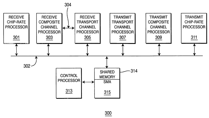
(0036] An overview of the preferred physical layer system architecture 300
is illustrated in Figure 2. The physical layer system can be used at either a
base
station/Node-B of a wireless communication system or at a user equipment. The
preferred architecture allows for flexibility in design of the physical layer
processing across differing wireless environments, such as TDD, FDD modes of
the proposed 3GPP W-CDMA system and GSM.
[0037] Blocks 301, 303, 305, 307, 309 and 311 represent a suite of software
parametizable leveraged embedded processors and are also known as virtual
circuits (VCs). A receive chip-rate processor 301 is connected to a data read
bus,
a data write bus and a control bus, hereinafter the three are to be known as
the
system bus 302. The receive composite channel processor 303 block and receive
transport channel processor 305 block are also connected to the system bus
302.
In addition, the two blocks also have a sequential number bus that reports to
the
receive transport channel processor 305 which data block is ready for
transport
channel processing. The transmit transport channel processor 307, transmit
composite channel processor 309 and transmit chip-rate processor 311 blocks
are
also connected to the system bus 302. The shared memory/ shared memory
arbiter (SMA) 315 block is connected to the system bus 302 and to the control
processor 313 block. In the preferred implementation, the block's
functionality is
-5-
CA 02482616 2004-10-14
WO 03/090011 PCT/US03/11415
designed to perform the physical layer processing of either TDD, FDD or both
modes of the 3GPP, although in other implementations other physical layer
processing approaches may be performed by the blocks.
[0038] The control processor 313 communicates with processing blocks via
control queues in the shared memory 314 via the SMA 315. The control processor
313 places set-up and control data into specific shared memory locations to
act as
data registers for each control block. The shared memory is also utilized as a
data block place holder to transfer data amongst the processing blocks. This
is
preferably achieved through linked lists which transfers data in blocks, with
the
last element of each block being an address of a next data block or an end of
data
indicator. This technique reduces buffering in the physical layer processor.
The
control processor 313 is preferably an advance RISC machine (ARM) processor.
Alternately, it may be any embedded processor.
[0039] The Shared Memory Arbiter (SMA) 315 is a hardware only virtual
circuit (VC) that controls access to a memory shared by the main VCs and the
control processor 313. The SMA unit contains address registers and the
sequencing logic necessary to allow all of the VCs and the processors to
efficiently
share access to the memory.
[0040] A high level block diagram of a SMA is illustrated by Figure 12.
The SMA unit contains address registers 601 and the sequencing logic necessary
to allow all of the VCs and the processors to efficiently share access to the
shared
memory 314. The SMA accepts one request into its pipeline every clock cycle ,
provided there are pending request(s). The SMA address generator maintains a
register for each SMA channel containing the address for the next memory
access
to be performed on that channel. These registers must be initialized to the
first
memory address of the memory block to be accessed. Each address register has
an associated control bit that is configured by software to indicate if an
address
pointer is to be incremented or decremented after each access.
[0041] There are three types of memory channels: 1) read channel data is
transferred from shared memory to the requesting unit, 2) write channel data
is
transferred from the requesting unit to the shared memory, and 3) control
-6-
CA 02482616 2004-10-14
WO 03/090011 PCT/US03/11415
channels (special read channels) support two types of memory access, read
access,
as for a normal read channel and load access. Load access is used to transfer
a
memory pointer from shared memory into one of the address registers in the
SMA. This allows an efficient implementation of a linked list.
[0042] Each hardware component is assigned one or more SMA channels,
and transfers to and from memory are controlled by a request/grant handshake
on each SMA channel. Request signals are prioritized in order to guarantee
timely access on critical paths. Once a request is in the pipeline, the same
request will not be accepted into the pipeline again, until the grant is sent.
[0043] When a receive chip rate processor 301 has completed its processing,
it will send a request 603 to the SMA. The SMA 315 will prioritize the request
603 and allocate a memory address via the address register 601 for the shared
memory 314. The SMA will then send a write grant 605 to the requesting source,
to begin data transfer.
[0044] One potential implementation for the physical layer processing
system is to process either or both the TDD and FDD modes of a 3GPP system.
In such an implementation, referring back to Figure 1, the various processing
blocks are divided into three general processes, transport channel processing
400,
composite channel processing 402 and chip rate processing 404. Transport
channel processing 400 is performed on the transport channels. Composite
channel processing 402 is performed on the composite channels and is performed
on a frame by frame basis and chip rate processing 404 is also performed on a
timeslot by timeslot basis.
[0045] As shown in Figure 1 for TDD and FDD uplink processing, the
transport channel processing performs the functions of CRC attachment 42,
transport block concatenation 44, channel coding 46, radio frame equalization
47,
first interleaving 48 and radio frame segmentation 50.
(0046] For the FDD downlink, the transport channel processing 400
includes the functions of CRC attachment 42, transport block concatenation 44,
channel coding 46, rate matching 52, first DTX indication insertion 72, first
interleaving 48, radio frame segmentation 50 and transport channel
multiplexing
_7_
CA 02482616 2004-10-14
WO 03/090011 PCT/US03/11415
54. It should be noted that in TDD mode, the de-rate matching 52 may be
performed in wither the transport or composite processor.
[0047] For the TDD mode and the FDD uplink, the composite channel
processing 402 performs the functions of rate matching 52, transport channel
multiplexing 54, physical channel segmentation 58,bit scrambling 55, second
interleaving 60 and physical channel mapping 62. For the FDD downlink, the
composite channel processing 402 performs the functions of second DTX
indication insertion 74, physical channel segmentation 58, second interleaving
60
and physical channel mapping 62. For the TDD mode and both the uplink and
downlink of FDD mode, the chip rate processing 404 performs the functions of
spreading 64, scrambling 66, pulse shape filtering 68 and frequency correction
70.
[0048] As shown in Figure 1, preferably TDD and FDD processing 400, 403
is handled by three sections: 1) a transport channel processing 401 section,
2) a
composite channel processing 402 section, and 3) a chip rate processing 403
section.
[0049] In the preferred architecture as shown in Figure 2, control blocks
are created for each of these sections for the transmit and receive
operations,
totaling six processing blocks (three transmit and three receive). The
operations
of these controls blocks is parametized. As a result, the manner at which
these
blocks operate can be changed by software. This allows for the same hardware
control blocks to be used in differing wireless environments. Software is used
to
reparameterize the control blocks based on the wireless system it resides.
[0050] An illustration of the flexibility of the control blocks is shown in
Figure 4, the physical layer processor capable of processing in both 3GPP FDD
and TDD modes. The receive composite channel processor 303, receive transport
channel processor 305, transmit transport channel processor 30?, transmit
composite channel processor 309, the control processor 313 (such as a ARM, DSP
or RISC processor) and shared memory/ SMA 315 are all utilized whether the
physical layer processor is operating in TDD or FDD mode. However, the
functions of each of these blocks are changed depending on the physical layer
_g_
CA 02482616 2004-10-14
WO 03/090011 PCT/US03/11415
processor operating mode. Therefore depending whether the mode of operation is
TDD, FDD or TSM, new reparameters are sent to the blocks allowing mode
change.
[0051] Since the transmission formats in TDD and FDD differ, the physical
layer processor has two transmit blocks, a TDD transmit chip-rate processor
311
and an FDD transmit chip-rate processor 306. Similarly, on the receive side,
two
receiver blocks are used, a TDD chip-rate processor 301 and a FDD receive chip-
rate processor 304. The TDD chip rate processor 301 detects TDD formatted
signals, such as by using a multi-user detection device. The FDD chip rate
processor 304 detects FDD formatted signals, such as by using a Rake receiver.
[0052] When the physical layer processor is operating in TDD mode, the
TDD receive chip-rate processor 301 and the TDD transmit chip-rate processor
311 are utilized along with the other six commonly utilized components. When
the physical layer processor is operating in FDD mode, the FDD receive chip-
rate
processor 304 and the FDD transmit chip-rate processor 306 are utilized along
with the other six commonly utilized components.
[0053] Since the only hardware difference required between the TDD and
FDD modes is the chip-rate receivers 301, 304 and transmitters 311, 306, by
using substantially the same hardware blocks either an FDD, TDD or both
FDD/TDD physical layer processor can be implemented. In an analogous
manner, these hardware blocks could be utilized for wireless systems other
than
the TDD and FDD modes of the 3GPP.
[0054] To implement a physical layer processor performing only TDD mode,
the hardware blocks of Figure 4 can be used without the FDD receive and
transmit chip rate processors 304, 306. Conversely, to implement a physical
layer processor performing only FDD mode, the hardware blocks of Figure 4 can
be used without the TDD receive and transmit chip rate processors 301, 311. As
a result, the receive composite channel processor 303, receive transport
channel
processor 305, transmit transport channel processor and transmit composite
channel processor 307 hardware implementations can be used in various wireless
environments.
_g_
CA 02482616 2004-10-14
WO 03/090011 PCT/US03/11415
[0055] Figure 4 is an illustration of the hardware components for either a
preferred FDD mode user equipment (LTE) or base station/Node-B. It should be
noted that the cell search 316 is only for UEs. Signals are received over an
antenna 317 or an antenna array of the user equipment/Node-B. An RF receiver
316 produces in-phase and quadrature baseband samples of the received signals.
[0056] The FDD receive chip-rate processor 301 comprises a cell search and
Rake finger locator 316, Rake fingers 312 and data estimator 314. The cell
search and Rake finger locator 316 performs cell selection and locates the
paths
of received communications to identify the phase delays for the Rake fingers
312.
The Rake fingers 312 collects the energy of the multiple paths of the received
signals. The data estimation 314 produces soft symbols of the received signals
for composite processing.
[0057] The receive composite channel processor 303 performs the composite
processing on the soft symbols produced by the data estimation 314. The
receive
transport channel processor 307 comprises a de-interleaver/de-rate matcher 52,
a
turbo decoder 41, a Viterbi decoder 43 and a CRC decoder 42. The de-
interleaver/de-rate matcher performs an inverse of the first and second
interleaving as well as an inverse of the rate matching. The turbo decoder 41
decodes turbo encoded signals and the Viterbi decoder decodes convolutionally
encoded signals 43. The CRC decoder 42 decodes the CRCs of the received
signals. Under the direction of the control processor 313 and SMA 315 control
316, the network data is recovered from the received signals using the FDD
receive chip rate processor 301, the receive composite channel processor 303
and
transport channel processor 305.
[0058] On the transmit side, the network data is processed by a transmit
transport channel processor 307, transmit composite channel processor 309 and
FDD transmit chip rate processor 311 to produce an in-phase and quadrature
signal. The transmit transport channel processor 307, transmit composite
channel processor 309 and FDD transmit chip rate processor 311 are directed by
the control processor 313 and MEM/SMA controller 316 to perform the proper
processing. The in-phase and quadrature signals are converted to a modulated
-10-
CA 02482616 2004-10-14
WO 03/090011 PCT/US03/11415
RF signal by a RF modulator 308 and radiated by an antenna 317A or antenna
array through the wireless interface.
[0059] Figure 6 illustrates how data is transferred between the shared
memory 314 and the composite blocks for transmission. For reception, the
process is performed in the reverse. For example, if the time transmission
interval (TTI) is set to 4, there are four transmit blocks TrBlkO -TrBlk3 251 -
257 of data to be processed. The SMA 315 places the memory into the transmit
buffer 265 of the shared memory 314. At each frame time, which is 10 ms, the
SMA 315 transfers the blocks of data to the transport channel processor 307,
where processing such as CRC attachment and channel coding occurs. When
processing is complete or just about finished, the SMA 315 moves the processed
data blocks into a first interleaver buffer 267within the shared memory 314.
Since the TTI is set to 40 ms In this example, the SMA 315 transfers one-
quarter
of the interleaver buffer 267 each 10 ms. (one frame) to the composite channel
processor 309. After processing is complete or just about compled, the SMA 315
places the results into a physical channel buffer 269 in the shared memory
314.
The frame's worth of data is then transferred into the chip rate processor 311
via
the SMA 315. The processed data is sent to an RF modulator to be radiated
through a wireless interface
[0060] Figure 7 illustrates the pipeline timing for the above transmit
processing with frames of ten milliseconds in length, as per 3GPP. Two
transport
channels and an associated coded composite channel are configured in frame N-2
295 and data is immediately sent on the channels. The transmit frame
components process data in frame N-1 296 and the transmit chiprate processing
operates in frame N 297, the first over-the-air (OTA) frame for coded
composite
transport channel_1 (CCTrCh_1). Each horizontal region represents a
computational component in the system and is a stage in the pipeline. The
activity of each processor is represented by boxes 401- 482, respectively. The
activity boxes in each horizontal region appear in the order in which they
will
typically occur in the system. The dotted lines with arrows represent time
dependencies. For example, when one processor ends a processing task, it
-11-
CA 02482616 2004-10-14
WO 03/090011 PCT/US03/11415
communicates to another processor so that the latter may begin its processing
task.
[0061] At time N-2 295, the configure transport channel 1 message is
received by transmit frame software 401. In addition the configure CCTrCh
channel 1 402, configure transport channel 2 403 messages are received by
transmit frame software. The transmit data for transport channel 1 406 and
transmit data for transport channel 2 407 are received by transmit frame
software.
[0062] At time N-1 296, the new configurations are merged into active
database 409. The transmit frame software writes a control block for transport
channel 1 to shared memory and then tells transmit transport processor to
begin
processing 411. The transmit frame software writes control block for transport
channel 2 to shared memory, then either links the new control block to the one
for transport channel 1 or tells transmit transport processor to begin
processing
413. The transmit frame software writes transmit composite control blocks for
CCTrCh 1 to shared memory and tells transmit Composite processor to begin
processing 415. The Transmit chip software writes control block for time slot
1 of
frame N to shared memory.
[0063] At time N 297, the transmit chip software writes control block for
time slot 2 of frame N to shared memory 419. The transmit frame software
begins to write transmit Composite control blocks for cctrch 1 to shared
memory
and tells transmit Composite processor to begin processing 421. The transmit
chip software interrupts transmit Frame software and writes control block for
time slot 2 of frame N to shared memory 423. The transmit frame software
completes writing Transmit composite control blocks for cctrch 1 to shared
memory and tells transmit composite processor to begin processing 425.
[0064] The transmit transport reads transport data for transport channel 1
and outputs four frames of interleaved data to shared memory 440. The transmit
transport reads control block and transport data from shared memory for
transport channel 2 and outputs four frames of interleaved data to shared
memory 442.
-12-
CA 02482616 2004-10-14
WO 03/090011 PCT/US03/11415
[0065] The transmit composite processor reads control blocks, 1st frame of
transport channel 1's output data, and 1st frame of transport channel 2's
output
data. It processes the data and writes resource unit data into shared memory.
The transmit composite processor must wait until the transmit transport
processor has completed writing interleaved data for both transport channel 1
and transport channel 2 460. The transmit composite processor reads control
blocks, 2nd frame of transport channel 1's output data, and 2nd frame of
transport channel 2's output data. It processes the data and writes resource
unit
data into shared memory 462.
[0066] The chip rate processor reads resource unit data for the first
timeslot of the first OTA frame of cctrch 1 and outputs soft symbols 480. The
transmit chip rate processor reads resource unit data for the second timeslot
of
the first OTA frame of cctrch 1 and outputs soft symbols. This is followed by
the
transmit chip rate processor reading resource unit data for the third timeslot
of
the first OTA frame of cctrch 1 and outputs soft symbols 482.
[0067] The preferred software design is for the transmit frame to be a
message based, event driven system, as shown in the top level state diagram in
Figure 8, with the system starting in wait for message loop 201. An arriving
configuration messages cause a state change in the wait for message loop 201,
bringing about a call to a service routine which places or updates data in a
database. For example, the system requires a hardware initialization, the
state
change is detected in wait for message loop 201 and a call to initialize
hardware
209 is performed. Upon return form the call, the update pending database 233
function is called and the hardware configuration data transfer to the
pertinent
database is carried out. When all configuration changes and data transfers are
carried out, the wait for message loop 201 calls the execute(1~ 225 function.
This
function causes a database register which holds information regarding what
database have been updated or changed since the last frame tick 203.
[0068] A frame tick occurs every 10 ms. in this 3GPP example and. is
detected by the wait for message loop 201. The system goes into a frame tick
203
subroutine. The databases that are semaphored in the database register from
-13-
CA 02482616 2004-10-14
WO 03/090011 PCT/US03/11415
the above execute(n) 225 function are updated 205 and a setup and start of the
data processing 207 is performed.
[0069] The additional states of configure TrCh 209, release TrCh 211,
configure radio link 215, release radio link 217, release physical channels
219 are
examples of other routines the message loop 201 look for. The TrCh Data 221
routine is the subroutine that sets up the block transfers.
[0070] Figure 5 is an illustration of control blocks and a linked list scheme
using a shared memory access scheme and of the present invention. A hardware
register 151 contains the beginning address of a memory control block 155.
When parameters and data span over two or more blocks, a linked list
mechanism allows for seamless transfers. For example, control block 155
resides
in memory as a linked list, its last entry there is a pointer to a second
control
block 165.
[0071] Memory access is provided by the processor 313 or the SMA 315.
For example, the hardware register 151 has the beginning address of control
block 155, which is loaded with parameters and data. In operation, consecutive
memory accesses by the SMA 315 or the processor 315 allow data transfers to
and from the composite blocks.
[0072] For example, the first set of parameters 154 in control block 155
start at address O100h. A memory address pointer is first set to O100h and
parameters 154 are transferred. The memory address pointer is incremented to
the next memory address, which is 0104h and parameters 157 are transferred.
This process is repeated until the memory addressing reaches address 0118h.
[0073] At OllCh the processor 313 or SMA 315 either by initial set up or a
by a flag in the data located at 011C8h, and, swaps the memory address pointer
with the first address of data block_1 162. The data in data block_1 is then
sequentially transferred. Upon completion of the transfer, the memory address
pointer is then swapped back and incremented and points to address 0120h of
control block 155, which also swaps the memory address pointers to
sequentially
acquire additional data from data block 2 164.
-14-
CA 02482616 2004-10-14
WO 03/090011 PCT/US03/11415
[0074] Upon returning from data block 2 164, the memory address pointer
is at 0124h which is the Next Chain_Address 160. The data located at this
address is the first address of to the next control block 165, which also
comprises
parameters 166 and data block addresses 168-174 pointing to data blocks 176-
180, respectively. At the end of this linked list is a flag 174 indicating the
end of
the link lists.
[0075] An illustration of a preferred block loading process from the shared
memory 315 is illustrated in Figure 10. In typical implementations, there are
timing issues associated with write accesses to dual port memories.
Contentions
come about when two or more entities try to access the same memory region,
especially when performing a write operation. One possible preferred approach
to resolve this problem is to allow control block writes when the
composite/transport processor is idle.
[0076] As a new block becomes available 202, a check is made to see if the
composite/transport processor is idle 204. If the composite/transport
processor is
busy, the chain pointer is overwritten 208 and the control loops back checking
to
check the status of the processor. If composite/transport processor is idle, a
shared memory access (SMA) pointer is written 206 and the data write is
started
210. A check for more control blocks 212 is performed. If there are more
control
blocks, control loops back to the check processor status 202. If there are
more
control blocks, the block loading is complete and the system will return 214.
[0077] A preferred embodiment for physical layer processing for
transmission in TDD mode is described as follows to illustrate the
parameterization of the control blocks. To generate transmittable data, the
control blocks transmit transport channel processor 307, transmit composite
channel processor 309, and transmit chip-rate processor 311 are utilized.
First
blocks of data are sent to the transmit transport channel processor 307 block
from the shared memory 315. Transport blocks are generated and a cyclical
redundancy check (CRC) is added at CRC attachment processor 42 to each new
transport block. In the preferred implementation, typical CRC types are
generated, including none, 8, 12, 16 and 24 bit CRCs.
-15-
CA 02482616 2004-10-14
WO 03/090011 PCT/US03/11415
[0078] Table 1 is a list of software parameters which is loaded into
transmit transport channel processor 307 block.
Control Block
Parameters Comments/Description
Quality of Service CRC. Number of CRC bits / 4
coding type. 00 = none. O1= turbo 10
= 1/2 conv. 11 = 1/3
cony.
interleave rate. 00=lOms. O1=20ms.
10=40ms.11=80ms.
Mode : NCOL-P (number of columns in the
interleaver matrix)
00=P. O1=P+1. 10=P+1 and K=C*R. 11=P-1.
MAC header pad bits
Sequence Number : used to identify each transport channel.
Number of Transport: Number of transport blocks in transport
channel.
Blocks
Transport Block : Number of bits in last 32-bit input
Size word. 0 means 32.
Number of bits per transport block.
Rounded up to the
next multiple of 32.
Coder Input Size : Number of total bits input to the
coder minus one.
Coder Output Size : Number of total 32-bit words output
from the first
interleaver.
Coding Block Size Number of bits per coder block.
Coding Block Filler: Number of filler bits in the first
Bits code block.
Turbo Interleaver : the Number of rows in the transport
Control channel.
Primitive Root.
Prime Number.
Turbo Interleaver Prime Number table for the turbo interleaver
Prime (10 words).
Number Table
Interleaver Memory Frame destination addresses, 8 addresses
regardless of
Addresses TTI.
Transport Block Transport block source addresses. One
Memory per transport
Addresses block.
Next TrCH Control Pointer to the control block for the
Block next transport channel
Address/End (if there are more to process). A NULL
(value of 0)
pointer with bit 31 set indicates that
there are no more
transport channels (i.e. a value of
0x80000000 is always
used to indicate the last transport
channel.
Table 1
-16-
CA 02482616 2004-10-14
WO 03/090011 PCT/US03/11415
[0079] The TrBlk concatenation/code block segmentation processor 44
creates a transmission time interval's (TTI's) worth of transport blocks,
where
the number of the blocks depends on the transport format selected for a
particular Transmit channel. The segmentation processor 44 also concatenates
the blocks into a single entity.
[0080] Code blocks for the given transport channel are delivered to the
channel codes processor 46. Depending on the coding type for the given
transport
channel, specified in the input data file, they are delivered to the
appropriate
channel codes function. Referring to Table 1, bits 10 and 11 are set to the
desired
type of coding. If the bits are set to 00, there is no coding. If the bits are
set to
01, 10 and 11, the coding is Rate 1/2 convolutional, Rate 1/3 convolutional
and
Turbo, respectfully. The types of coding which are possible in the preferred
embodiment are defined by the 3GPP TSG-RAN "Muliplexing and Channel
Coding" 3GPP TS 25.212. This parameterizable hardware based approach allows
for coding at a high performance level, for example, one clock per bit for
convolutional encoding and two clocks per bit for Turbo Encoding. This is ten
to
one-hundred times faster (per clock rate) than the same function is typically
performed in software.
[0081] After channel coding, the coded blocks are processed in sequence by
a rate matching process in the radio frame equalization 45 process. This
effectively implements a concatenation of encoded blocks. The output is then
sent to a first interleaves 50 process. The interleaving depends on the TTI
interleaves rate which is also a software parameter in Table 1. For example, a
00
is set into bits 8 and 9 of the Quality of Service register for an interleave
of 10
milliseconds. For 20, 40 and 80 ms TTIs, values of Ol, 10 and 11,
respectively,
are set into bits 8 and 9. The data is segmented in the radio frame
segmentation
process 50 and returned to the shared memory 315 ready for the transmit
composite channel processor 309 block.
[0082] The transmit composite channel processor 309 block extracts data
from the shared memory 315 along with control parameters and produces
physical channel data. A radio frame's worth of data is complied from the data
-17-
CA 02482616 2004-10-14
WO 03/090011 PCT/US03/11415
output from the previous block's first interleaver for the given transport
channel.
[0083] Table 2 is a format parameter table of the transmit composite
channel processor's 309 control block.
TrCH Control Description
Block Parameters
Number Bits BeforeThe Number of bits in the current column
(frame) of the
Rate Matching First Interleaver Buffer for this TrCH.
This
Trch
Number Leftover The Number of bits at the tail of the
transport channel
Bits This Trch that are not considered for puncturing
or repeating.
Used for Turbo puncture, P2 bits.
Rate Matching Indicates whether the bit sequences is
{S,P1,P2}
Direction (forward) or {P2,P1,S} (reverse) Used
for Turbo
puncture, P2 bits.
Rate Matching Indicates TURBO PUNCTURE, REPEAT,
Type
NON TURBO PUNCTURE, or NONE.
Rate Matching Indicates whether the first bit in the
column is a
Column Top systematic (S), parity 1(P1), or parity
2 (P2) bit.
std_e initl The initial value of the rate matching
parameter for the
first sequence.
std_e_plusl The increment value to the error when
a bit is punctured
or repeated.
std_e_minusl The decrement value to the error when
a bit is read from
the First Interleaver Buffer.
std a init2 The initial value of the rate matching
parameter for the
second sequence. Used for Turbo puncture,
P2 bits.
std_e_plus2 The increment value to the error when
a bit is punctured
or repeated. Used for Turbo puncture,
P2 bits.
std_e_minus2 The decrement value to the error when
a bit is read from
the First Interleaver Buffer. Used for
Turbo puncture,
P2 bits.
Start Address The starting memory address of the transport
This channel.
Trch
Table 2
[0084] For example, the rate matching type parameter uses bits 28 and 29.
When these bits are set to 00, this indicates TURBO PUNCTURE mode.
-18-
CA 02482616 2004-10-14
WO 03/090011 PCT/US03/11415
Likewise, REPEAT, NON TURBO PUNCTURE, and NONE are represented by
placing O1, 10 and 11, respectively into bit locations 28 and 29 of the
parameter
register.
[0085] The data is rate matched by rate matching process 52 before it is
multiplexed with other channels at the transport channel (TrCH) multiplexing
process 54. The output of the multiplex transport channel processor 54 is
segmented into physical channels in the physical channel (PyCH) 57 processor.
A second interleaving is performed by the second interleaving processor 46 and
mapped into physical channels at the physical channel processor 62. The
transmit channel processed data is then returned to the shared memory 315 for
further processing by the transmit chip-rate processor.
[0086] The transmit chip-rate processor 311 block then extracts data and
control parameters from the shared memory 315. In the preferred TDD
implementation, the block 311 performs spreading, scrambling, gain
application,
formatting, preamble insertion, RRC filtering and produces one to sixteen
resource units per time slot. The I and fl output of the transmit chip-rate
processor 311 for transmission.
[0087] Figure 11 illustrates a preferred transmit configuration timeline 500
and show the advantages of the reparamatizable hardware implementation. The
frames are bound by Frame Markers 503 on the Message Timeline 502. To
transmit a signal at Frame N 409, the data for the transmission must be
configured during Frame N-2 505 before the processing is started at Execute N
510. The data for Frame N is processed during Frame N-1 and must be
completely finished processing and ready to transmit by Frame Marker 503(n).
[0088] At time N-2 505 on the database timeline 504, the frame hardware
of the transmit channel is configured. At time N-1 507 the start control
signal is
sent from the SMA 313 to start the block processing from the database. The
processing is performed in the transmit transport channel processor 307 and
transmit composite channel processor 309, which make up the transmit frame
receive processors. At time N 509, the transmit chip processor 311 is
processing
the data it received from the database.
-19-
CA 02482616 2004-10-14
WO 03/090011 PCT/US03/11415
[0089] To illustrate the flow of data through physical channel processing,
Figure 12 is an illustration of a preferred flow of data for FDD transmission.
In
Figure 12, the transport channel is encoded and interleaved by a factor of
four
into two physical channels. The raw data for transport channel_1 102 and
transport channel 2104 are SMA transferred to the transport channel processing
106 where the CRC is added and the data is segmented into code blocks. The
blocks are encoded, rate matched and a first interleaving is performed. The
data as blocks of transmit channel data 108 - 122 are sent to the shared
memory.
The data is then sent to composite channel processing 124 where it is rate
matched, second interleaved and segmented into physical channels at the rate
of
once per frame. The Physical Channel data is sent to the shared memory ordered
as physical channels by frame 126 - 128. The physical channels by frame data
is
then sent to the Chip Rate Processing 130 where it is spread scrambled and
filtered on a per frame basis. A control channel is also appended to each
generated frame.
[0090] A series of "jobs" for each channel processor are scheduled by
software and presented to the processors via linked list job queues maintained
in
the shared memory. Each processing unit receives "jobs" via control blocks
that
reside in the shared memory. The content of each control block is a function
of
the unit for which it controls. The data and the order of the data is defined
by
the functionality and the specifications of each unit. Entries in each control
block
include control parameters for the unit and addresses which point to input
data
and addresses to output data locations. Control blocks can be linked together
reducing control processor overhead.
[0091] With respect to the physical layer processing of received signals in
TDD mode, a preferred parameters table is shown in Table 3.
-20-
CA 02482616 2004-10-14
WO 03/090011 PCT/US03/11415
Name Description
i12 Disable Second Interleaver disable.
Descr Disable Descrambler disable.
Number TrCH Number of TrCH in the CCTrCH.
Number Interleaver Blocks Number of ILBs in the CCTrCH.
Interleaver Block Size Number of bits in this ILB.
Number Ts Blocks Number of time slots in the
ILB.
Number Full Columns Number of full columns in the
second
interleaver matrix.
Number Rows Number of rows in the interleaver
array
of 30 columns.
Ts Block Size Time slot data block size in
bits.
Number resource units (RUs)Number of RUs in the time slot.
RU Size RU data block size (number of
soft
decisions).
RU ConsecutiveSize Number of consecutive soft bits
read from
RU.
RU Offset Offset from the start of the
first data word
of an RU which has data mapped
in
reverse order.
RU Address Start address of the RU data.
RU Direction Data for an RU can be mapped
in
Forward or Reverse order.
Table 3
[0092] For example, to disable the second interleaving, bit 16 of the "12
Disable" would be set to a 1. Control parameters and blocks of data are
transferred from the shared memory 315 to the receive composite channel
processor 303 block.
[0093] Figure 13 represents the receive configuration timeline 700. The
frames are bound by frame markers 703 on the message timeline 702. When a
received signal is captured at Frame N 705, the received data is processed
during
frames Frame N+1711 and Frame N +2 713. At Frame N+3 the received data is
ready for high layer processing.
-21-
CA 02482616 2004-10-14
WO 03/090011 PCT/US03/11415
[0094] At time N-1 703, the software parameters for hardware
configuration for a particular received frame must be available in the pending
database. At time N 709, the receive chip rate processor 301 places the data
into
the database. At time N+1 711, the received frame processor, which are
comprised of the receive composite channel processor 303 and receive transport
channel processor 305 process the received data and subsequently sends the
data
on to higher layers.
-22-