Note: Descriptions are shown in the official language in which they were submitted.
CA 02482724 2004-09-28
Stress-Induced Control of Polarization Dependent Properties in Photonic
Devices
FIELD OF THE INVENTION
[00011 This invention relates to photonic devices with controlled polarization
dependent properties and methods of making the same.
BACKGROUND OF THE INVENTION
[00021 In photonic devices incorporating waveguides, mode transmission is
affected
both by the material anisotropy, and by the cross-sectional geometry of
waveguides..
An example of the structures under discussion is illustrated schematically in
Fig. 1.
The waveguides include a core and cladding layers and generally interfaces
between
the core and cladding layers impose different boundary conditions for modes of
propagation with different polarizations. These effects induce a polarization
dependent loss (PDL), and a polarization dependent refractive index.
100031 Modes with electrical field polarized perpendicular to the wafer plane
are
defined herein as TM, and parallel to the wafer plane as TE. The modal
birefringence
is defined as Anef = neff "~- neff , where nef TM and neif E are the effective
indices for
the TM-like and TE-like modes in the channel waveguide. In many types of
integrated
optical device, it is critical to either eliminate, the birefringence
altogether, or to adjust
it to a given value.
[00041 Optical waveguide components and devices for communication applications
are
required to be polarization insensitive. As communication systems advance, the
tolerance for polarization sensitivities becomes more stringent. Planar
waveguide
technology has made significant progress in replacing discrete photonic
devices, such
as thin film and bulk-optic components. The demand for increased functionality
and
1
CA 02482724 2004-09-28
reduced cost continues to drive the downscaling of device sizes, which can be
achieved by reducing waveguide cross-section areas in high index contrast
(HIC)
material platforms.
[0005] Highly compact photonic devices can be implemented in high index
contrast
(HIC) material systems such as silicon-on-insulator (SOI), SiN on SiO2, and
III-V
semiconductors. In state-of-the-art commercial devices using SOI, the core
size is
typically on the order of 5 gm and the geometrical birefringence can be
minimized to
an acceptable level by changing the cross-sectional dimensions of the
waveguides.
This technique is sufficient for devices with large core size, since their
geometrical
birefringence is relatively low. Such devices, however, are of comparable size
to
those based on glass waveguides, and the size-reduction potential of SOI is
unutilized.
[0006] One source of modal birefringence in channel waveguides is solely
caused by
the cross-sectional geometry of the waveguides, herewith denoted as
geometrical
birefringence AngeO. As the waveguide size is reduced, Angeo can become very
large as
shown in Fig. 2. Although the condition for birefringence-free propagation may
still
exist, the birefringence becomes very sensitive to the fluctuations in the
waveguide
dimensions. To achieve control within the tolerance range of state-of-the-art
photonic
devices, cross-sectional dimension control in the order of 10 rim is required.
This
stringent requirement is technologically a challenge and may be very expensive
to
implement. Furthermore, ridge dimensions also determine the number of
waveguide
modes, the minimum bend radius, and the mode size. It is often impossible to
simultaneously meet several design objectives, including zero birefringence,
using
waveguide dimensions alone. These are some of the reasons why small-size SOI
2
CA 02482724 2004-09-28
waveguide devices are not currently available commercially. Viable means of
producing polarization insensitive devices or providing birefringence tuning
are
required.
[00071 Current practice to either eliminate birefringence, or to adjust the
birefringence to a desired level (D. Dimitropoulos, V. Raghunathan, R. Claps,
and B.
Jalali, `Phase-matching and nonlinear optical processes in silicon
waveguides', Optics
Express 12(1), p. 149, 2004) is to adjust the waveguide width to depth ratio
(L.
Vivien, S. Laval, B. Dumont, S. Lardenois, A. Koster, and E. Cassan:
"Polarization-
independent single-mode rib waveguides on silicon on insulator for
telecommunications wavelengths", Opt. Commun. 210, p. 43, 2002). Limitations
of
this method on the associated stringent requirement on dimensional
inaccuracies are
beginning to be recognized (Daoxin Dai, Sailing He, `Analysis of the
birefringence of
a silicon-on-insulator rib waveguide', Applied Optics 43(5), p. 1156, 2004.
100081 In conventional HIC waveguides where the core size is in the order of 5
m,
geometrical birefringence is on the order of 10-4. Satisfactory control can be
achieved
by adjusting waveguide cross-sections. This technique is sufficient for
devices with
large core size, since the geometrical birefringence is relatively low,
waveguide
modes are well confined within the core area, and generally large bend radii
are used.
[00091 With reducing waveguide core size, the geometrical modal birefringence
dngeO
increases drastically. The rate of change with dimensions also becomes very
large. In.
Fig. 2, the birefringence change with waveguide dimensions is shown for an
example
of waveguide cross-section, but similar dependence can be found in other types
of
cross-sections when waveguide dimensions are reduced. By choosing the ridge
aspect
3
CA 02482724 2004-09-28
ratio appropriately, the birefringence may in principle be eliminated. For a
given
waveguide width W, an aspect ratio may exist at which the orthogonally
polarized
modes becomes degenerate (i.e. birefringence-free), as indicated by the
circles in Fig.
3. Obviously, for waveguides with high geometrical anisotropy (e.g. for W
>>H), this
particular condition may not be possible to fulfill.
[00101 Ridge dimensions also determine the number of waveguide modes, the
minimum usable bend radius and the mode size, as well as the birefringence. It
is
often impossible to simultaneously meet several design objectives, including
zero
birefringence, using waveguide dimensions alone.
[0011] Ridge dimensions also determine the sensitivity of birefringence to
dimension
fluctuations, as illustrated in an example in Fig. 3 for etch depth and
waveguide
width. Wide waveguides (W>H) are less sensitive to dimension changes, and
offer
better process latitude. Unfortunately, the condition for Angeo 0 may cease to
exist.
SUMMARY OF THE INVENTION
[00121 The invention makes use of stress fields in the design of waveguides to
control
polarization dependant loss and polarization dependent refractive index. In
accordance
with the principles of the invention cladding stress induced birefringence is
taken into
account in the waveguide design, enabling the birefringence to be decoupled
from
geometrical constraints. The novel technique achieves the final desired
birefringence
with a combination of the stress-induced and geometrical birefringence.
Waveguide
dimensions can thus be optimized to meet other design criteria, giving an
enhanced
degree of design freedom.
4
CA 02482724 2010-02-12
[00131 Waveguide birefringence is the sum of geometrical birefringence and
stress-
induced birefringence. The importance of stress-induced birefringence in SOI
waveguides has not been recognized in the current literature. Geometrical
asymmetry
was thought to dominate (Daoxin Dai, Sailing He, `Analysis of the
birefringence of a
silicon-on-insulator rib waveguide', Applied Optics 43(5), p. 1156, 2004).
[00141 In one aspect the invention provides a method of making a photonic
silicon-
on-insulator (SOI) device incorporating a silicon-on-insulator waveguide
having a
waveguide core, comprising: a) designing a high index contrast silicon-on-
insulator
waveguide with a predetermined cross sectional geometry and dimensions
optimized
for design criteria other than final birefringence; b) determining the
geometrical
birefringence of the waveguide designed in step a); c) determining a target
amount,
which may be zero, of overall birefringence desired in said waveguide; d)
determining
an amount of stress to be induced in said waveguide core to achieve a stress-
induced
birefringence such that a combination of said stress-induced birefringence and
said
geometrical birefringence results in a final birefringence equal to said
target amount;
e) fabricating said waveguide; and f) inducing within said waveguide the
amount of
stress determined in step d).
[0015] A device employing a cladding material with unspecified stress using
this
technique would have an exhibited a final specified birefringence not in
accordance
with the geometrical birefringence of the phase controlling section of the
waveguide
device. It is non-trivial to determine the stress on a processed device. On
the other
hand, geometries and the composition of materials (core, cladding) are
straight
forward to determine. Once the geometry and the materials are known (therefore
the
material refractive indices), the geometrical birefringence is deterministic.
5
CA 02482724 2010-02-12
[00161 In another aspect the invention provides a photonic device, comprising:
a high
index contrast waveguide formed on a silicon-on-insulator substrate with a
core
having an inherent birefringence predominantly determined by cross-sectional
geometry and dimensions; wherein said core has a cross-sectional geometry and
dimensions that are optimized for design criteria other than final
birefringence;
wherein said waveguide comprises one or more cladding layers that are stressed
to
create a predetermined stress-induced birefringence in said core; and whereby
said
device has an exhibited final birefringence that is the result of said
inherent
geometrical birefringence and said stress induced birefringence caused by said
one or
more cladding layers.
[00171 It will be appreciated that in some case it may be desirable to adjust
the
birefringence to a specified value; on other cases it may be desirable to
adjust it to
zero, and the latter is clearly contemplated by the invention.
5a
CA 02482724 2004-09-28
100181 Cladding materials used in planar waveguides usually have different
thermal
expansion coefficients than the core material that consequently induces stress
in the
waveguides. Intrinsic stress can also be present. Through the photoelastic
effect, the
stress causes optical anisotropy, and renders the waveguide materials
birefringent. The
effective indices of the modes are hence modified. By choosing the correct
magnitude
and sign of the stress (being tensile or compressive), and appropriate local
stress field,
waveguide birefringence can be tuned for any waveguide shape and dimensions.
Birefringence-free operations can be extended to waveguides with non-zero
geometrical
birefringence.
BRIEF DESCRIPTION OF THE DRAWINGS
[00191 The invention will now be described in more detail, by way of example
only,
with reference to the accompanying drawings, in which:-
[00201 Fig. I is a schematic cross-section of a channel waveguide using the
SOI platform.
100211 Fig. 2 shows the dependence of birefringence on the core thickness H.
100221 Fig. 3 shows the variations of Ange0 with the ridge etch depth, for 3
different waveguide widths W.
100231 Fig. 4 shows the cross-section and stress distributions of a SOI ridge
waveguide.
100241 Fig. 5. (a) shows the modal birefringence Oneff of a waveguide with
oxide
claddings, as a function of the upper cladding thickness and stress level.
[00251 Figs. 5b to 5e show different waveguide profiles.
6
CA 02482724 2004-09-28
[0025] Fig. 6 shows the calculated change in modal birefringence as a
function of ridge etch depth (D=H - h) with a 0.7 .tm thick oxide cladding
film.
[0026] Fig. 7 (a) shows the variation of birefringence with SiO2 cladding
thickness for a wet etched SOI ridge waveguide, and (b) TE and TM channel
spectra for an SOI AWG compensated using 0.3 (top right) and 0.8 p.m
(bottom right) thick SiO2 claddings.
[0027] Fig. 8 shows the calculated (solid lines), and measured &. values (data
points) for AWGs with rapid thermal anneal tuning (RTA).
DETAILED DESCRIPTION OF THE PREFERRED EMBODIMENTS
[0028] Figure 1 shows a typical waveguide structure comprising a silicon
substrate
10, a lower SiO2 cladding layer 12, a core layer 14 with ridge 14a, and an
upper SiO2
cladding layer 16. The upper cladding 16 has a thickness oft; etch depth is
D=H-h.
[0029] Figure 2 shows the dependence of birefringence on the core thickness H.
In this
example, the waveguides have the same width as the core thickness H, and are
etched to
half the thickness. Similar dependence is found in other waveguide cross-
sections.
[0030] Fig. 3 shows the variations of Angeo with the ridge etch depth, for 3
different
waveguide widths W. In this example, the core thickness is 2.2 Am. The circles
indicate the birefringence-free points.
[0031] In such a waveguide structure stress-induced changes in material
refractive
indices are given by:
nx - nxo _ -C 16X- C2(6y + c) (I a)
7
CA 02482724 2004-09-28
ny- no = -CI6y- C2(6Z + 6x) (I b)
100321 Therefore:
nx - ny = (C I - C2)(Gy - (s) (2)
Here o is the stress tensor, n; the material refractive index, n;o the stress-
free refractive
index, and C 1 and C2 the stress-optic constants. These changes in material
indices
result in modified effective indices of the waveguide modes (neff E and
neflTM), and the
corresponding modal birefringence denoted as Oneff. This parameter is
determined by
both the ridge geometry and the stress distribution.
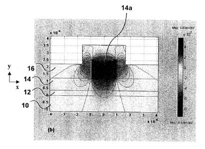
100331 An example of cladding induced stress field in SOI waveguides is shown
in
Figs. 4a and 4b. Here the cladding material is SiO2, which is commonly used.
Other
types of materials such as silicon nitride may also be used as cladding. The
upper
cladding is deposited after the formation of the waveguide ridge. Common
deposition
methods include PECVD (plasma-enhanced chemical vapor deposition) and LPCVD
(low pressure chemical vapor deposition), with wafers usually processed at
elevated
temperatures. It will be appreciated that other suitable deposition methods
can be
employed.
[00341 In the structure shown in Figures 4a and 4b, the buried oxide thickness
(lower
cladding 12) is 0.37 gm, top Si (core layer 14) thickness is 2.2 gm, ridge 14a
width is
1.83 gm, etch depth is 1.34 gm, upper oxide cladding (layer 16) thickness is I
gm.
8
CA 02482724 2004-09-28
Figure 4a shows the stress distribution in the x direction; Figure 4 b shows
the stress
distribution in the y direction.
[00351 The larger thermal expansion coefficient of SiO2 than that of Si is the
main
reason that a compressive stress resides in the oxide film when the samples
are cooled
to room temperature. Other than the miss-match of thermal expansion
coefficients
between different films, the stress is also affected by the film
microstructure and
stoichiometry. In the absence of a ridge, the stress in the cladding film is a
material
related parameter, determined by the deposition conditions and material
properties.
For SiO2 films, the stress usually varies from -100 MPa to -400 MPa, although
other
stress values may be obtained if so desired by changing processing conditions.
From
the modified index distribution, the corresponding effective indices and modal
birefringence can be calculated. Examples of the calculated birefringence
results are
shown in Fig. 5.
100361 As illustrated in Figs. 5a to 5e, a cladding with compressive stress
induces a
positive shift in Anff. Fig. 5(a) shows the modal birefringence Anff of a
waveguide with
oxide claddings, as a function of the upper cladding thickness and stress
level. The stress
in the oxide is compressive (negative), and stress levels shown represent the
in-plane
stress values in the absence of a Si ridge; Figures 5b to 5e shows other
examples of
channel waveguides: (b) vertical ridge; (c) trapezoidal ridge (arbitrary
angle); (d) vertical
rib; and (e) trapezoidal rib (arbitrary angle).
[0037] This shift increases with the cladding thickness initially, and
eventually reaches a
plateau. If a cladding material with tensile stress (such as silicon nitride)
is used, a
negative shift in Aneff is induced. This therefore provides two tuning
parameters: one is
9
CA 02482724 2004-09-28
the cladding thickness; the other is the cladding stress magnitude and sign.
Waveguide
profiles shown in Fig. 5 (b)-(e) typically lead to different MgeO. Depending
on the value
and sign of MgeOi an appropriate cladding can be chosen to meet the
birefringence-free
requirement Meff =0.
[00381 As can be observed in Fig. 5, cladding films with lower stress levels
give finer
tuning resolution but limited tuning range. Changes in thickness give larger
tuning for
small cladding thicknesses, and An& practically varies linearly with the
thickness. While
for thicknesses where Meff approaches the plateau finer tuning resolution can
be
obtained. Different combinations of these parameters can be selected to
optimize the
tuning sensitivity and tuning range, giving enhanced flexibility.
100391 Eq. (2) shows that the material birefringence scales linearly with the
stress
tensor. Due to the large index contrast in HIC waveguides such as SOI, the
cladding
stress induced index changes are typically orders of magnitude smaller than
the value of
the index contrast. Consequently, the stress causes little change in the mode
shape. Our
simulations have revealed that the modal birefringence Meff can be considered
to scale
linearly with the stress magnitude for a fixed cladding thickness for
practical designs.
Due to the minimum change in mode shape caused by the stress, there is also
little
mode-mismatch induced polarization dependent loss (PDL), and negligible mode
mismatch loss between sections of waveguides with different stress levels.
[00401 Stress-induced birefringence has been used to reduce the birefringence
in
silica-on-silicon waveguides. This issue, however, has not been addressed in
the SOI
system. In silica-based waveguides where index contrast is low, large cladding
thickness is required as the optical field penetrates deeper into the
cladding. Required
CA 02482724 2004-09-28
cladding thicknesses are so large that changing the thickness has little
effect on the
birefringence.
[0041] As it is demonstrated in this invention, tuning cladding thickness for
birefringence control is an efficient technique for HIC waveguides where the
optical
field is largely confined within the core area, and its penetration into the
cladding is
weak. The invention is described for the particular case of SOI waveguides,
but the
same principle is also applicable to other HIC waveguides.
[0042] As discussed above and illustrated in Fig. 3, waveguide aspect ratios
determine
the sensitivity of birefringence to ridge dimensions. Wide waveguides (W>H)
are less
sensitive to dimension fluctuations (e.g. etch depth change as shown in Fig.
6).
However, a negative Angeo persists. By incorporating a cladding layer with
compressive stress, the modal birefringence Anff can be eliminated, as shown
by the
curves for W=2.5 gm guides in Fig. 6. In this example the oxide cladding film
was 0.7
gm thick, the ridge height (H) 2.2 gm, and ridge width (W) 1.6, 2.0, and 2.5
m,
respectively. The solid curves show the modal birefringence including both
geometrical and stress-induced birefringence for an oxide stress of 6film = -
70 MPa;
the dashed curves show the waveguide birefringence in the absence of stress.
Significantly improved process latitude can be obtained.
[0043] Prototype arrayed waveguide grating (AWG) demultiplexers have been
produced which demonstrated the proposed techniques of birefringence control.
In
AWG demultiplexers, modal birefringence is determined from the polarization
dependent wavelength shift (AX) between the central wavelengths for TM and TE,
modes (& =A,TM-XTE), which is related to the waveguide birefringence in the
arrayed
11
CA 02482724 2004-09-28
grating section by Aneff= ng &.JX0 (X0 is the wavelength in vacuum, ng is the
waveguide group index).
[00441 Using AWG demultiplexers fabricated on SO] substrates, the inventors
have
shown (Fig. 7) that AX in AWGs can be varied over a wide range by changing top
oxide
thickness for a given stress level. With appropriately chosen oxide thickness
and stress
level, polarization sensitivity was virtually eliminated. The polarization
induced
channel wavelength shift, shown in Figure 7(b), was reduced to 20 pm by
depositing a
0.8 .tm cladding oxide with a stress of -320 MPa. Without the upper cladding,
AX was
approximately -0.54 nm. PDL was also negligible in these devices.
[00451 Post-process tuning can be achieved by adding or removing the
appropriate
thickness of the cladding layer. It can also be accomplished by changing the
cladding
stress using techniques such as thermal treatments, and IR or UV irradiations
etc. The
inventors have demonstrated post-process tuning of birefringence using rapid
thermal
anneals (Fig. 8). Thermal anneals decreased the stress in the oxide film,
which in turn
reduced AX. In the example shown in Fig. 8, AX was reduced by RTA from 0.3 nm
to
below 0.1 nm. ). Initial top cladding oxide thickness was 0.35 m and the
stress was -
335 MPa (compressive). The anneals were done at 600 C in nitrogen ambient.
[00461 Because of the large cladding-core index step, there is virtually no
change in
optical mode shape, and hence no mode-mismatch loss, between the SOI
waveguides
with and without a stressed cladding. A low polarization dependent loss (PDL)
is
expected. Stress-engineering provides an effective means of birefringence
control
while incurring negligible mode-mismatch loss. This makes it a superior
technique
compared to other methods.
12
CA 02482724 2004-09-28
[0047] Compared to other compensation method where regions with modified
birefringence are introduced, this method mitigates the birefringence directly
at its
source, i.e. in the waveguides, which are the basic building elements of
integrated
optic circuits. The invention is broadly applicable in waveguide devices.
[00481 In the context of the discussion of this invention, the example of SOI
channel
waveguides with oxide SiO2 cladding layers is used. However, the same design
constraints and the principles of this invention also apply to other high-
index-contrast
(HIC) waveguide systems
[00491 It will now be understood that the invention incorporates cladding
stress in the
design of waveguides, and in particular HIC waveguides, to allow for the
further
optimization of other design criteria, such as mode shape and waveguide bend
radii
with the waveguide's cross-section, and tolerance to the fabrication error in
waveguide dimensions.
[0050] The invention permits birefringence free operations to ensure by
selecting
suitable tensile or compressive stress with the appropriate magnitude in the
cladding.
Selecting appropriate combinations of cladding thickness and stress level
optimize the
tuning range and sensitivity. The cladding thickness and stress magnitude can
also be
employed as part of a post-process tuning process.
[0051] The invention is applicable to photonic devices incorporating a
waveguide,
including and not limited to interferometric-based devices, such as the Mach-
Zenhder
interferometer, ring resonator, arrayed-waveguide-grating, truncated arrayed
waveguide grating, and components requiring accurate phase matching, such as
silicon Raman amplifiers.
13