Note: Descriptions are shown in the official language in which they were submitted.
CA 02482803 2004-10-15
WO 03/090383 PCT/US03/11917
SYSTEMS AND METHODS FOR COMPENSATING FOR SIGNAL TRANSIENTS
BACKGROUND OF THE INVENTION
Field of the Invention
The present invention relates generally to optical systems and, more
particularly, to systems and methods for
compensating for the effects of transients in an optical system.
Description of Related Art
In the field of fiber optic communications, systems transmit wavelength-
division multiplexed (WDM) optical
signals along optical fibers to increase the capacity of an optical
communications link. A WDM signal includes
multiple distinct wavelengths of light. Each of the wavelengths carries a
respective optical information signal, known
as an information "channel." , The number of wavelengths (i.e., information
channels) in a WDM signal is a system
parameter and usually ranges from 2 to 128 or more (in the case of "dense" WDM
(DWDM)).
As the WDM signal travels through an optical network, it gradually fades and
is, therefore, amplified at
various points along its route. Because of the large number of wavelengths
that can be carried by a single WDM
signal, and also due to the high data rates of the individual information
channels, amplification is typically performed
by optical means.
Optical amplifiers can perform signal amplification using a doped length of
optical fiber. Suitable candidate
doping components for achieving optical amplification are rare earth doped-
fiber amplifiers, such as erbium doped-
fiber amplifiers (EDFAs). In an amplifier, it is possible to set the total
output power level of the amplifier to a desired
value, thereby establishing a relationship between the power of a WDM input
signal entering the amplifier and the
power of a WDM output signal exiting the amplifier. This also establishes a
gain relationship for the information
channels passing through the amplifier.
Ideally, the gain applied by the amplifier to the information channels remains
at a constant value. Transients
caused by the instantaneous addition or removal of one or more individual
optical information channels affects the-
power of the WDM input signal. Although the amplifier instantaneously reacts
to such a change in input power by
providing a corresponding change in output power, thereby maintaining a
constant gain for a brief amount of time, a
natural recovery process is initiated soon thereafter by the amplifier,
whereby the specified total output power
eventually becomes redistributed among the new number of wavelengths (or
information channels).
In the case of a channel being dropped, the effect of this transient will be
an eventual increase in gain for the
remaining information channels as the amplifier settles into steady-state
operation. Conversely, in the case of an
optical information channel being added, the specified total output power is
shared (possibly unevenly) among the now
larger number of wavelengths, leading to a decrease in gain for the
information channels as the amplifier reaches a
steady state.
The characteristics of these transients may depend upon the physics of the
amplifiers, the number of
amplifiers present, and possibly the distance between the amplifiers. Improper
handling of the transients may result in
degradation in the quality of the information channels reaching downstream
components of the fiber optic network.
As a result, there exists a need for systems and methods for compensating for
transients in an optical system.
CA 02482803 2011-05-31
SijNWARY OF THE INVENTION
Systems and methods consistent with the present invention address this and
other needs by providing transient
compensation logic that compensates for the presence of transients associated
with optical signals.
In accordance with the principles of this invention as embodied and broadly
described herein, a system
compensates for the presence of power transients. The system receives a data
signal and detects the occurrence of a
power transient. The system generates a threshold signal based on the detected
power transient and determines a value
of the data signal based on the threshold signal.
In another implementation consistent with the present invention, a terrestrial
terminal connects to an optical
underwater network. The terrestrial terminal includes a transmitter and a
receiver. The transmitter is configured to
convert terrestrial signals into an optical format for transmission to the
optical underwater network. The receiver is
configured to receive an undersea optical signal from the optical underwater
network. The receiver includes a filter,
an optical-to-electrical converter, signal conditioning logic, and
demultiplexing logic. The filter is configured to filter
the optical signal. The optical-to-electrical converter is configured to
convert the optical signal to an electrical signal.
The signal conditioning logic is configured to process a data signal from the
electrical signal, detect occurrence of a
power transient, and generate a threshold signal based on the detected power
transient. The demultiplexing logic is
configured to receive the data signal and the threshold signal from the signal
conditioning logic and determine
characteristics of the data signal based on the threshold signal.
According to an aspect of the present invention there is provided a receiver
for
compensating for optical power transients, comprising:
demultiplexing logic configured to:
receive a data signal which fluctuates in response to the power transient,
receive a threshold signal, and
determine characteristics of the data signal based on the threshold signal;
and
conditioning logic configured to:
detect occurrence of a power transient,
generate the threshold signal based on the detected power transient,
generate a threshold value which is adjusted to compensate for long-term
changes
in the signal power, and
generate a compensation signal compensating other changes of the power
transients, said threshold value and said compensation signal being added to
generate the
threshold signal sent to the demultiplexing logic.
According to another aspect of the present invention there is provided a
method for
compensating for power transients, comprising:
receiving a data signal;
detecting an occurrence of a power transient;
generating a threshold signal based on the detected power transient; and
determining a state of the data signal based on the threshold signal;
generating a threshold signal which value is adjusted to compensate for
longterm changes
in the signal power;
generating a compensation signal compensating for other changes of the power
transients;
and
adding said threshold value and said compensation signal to generate the
threshold value.
According to a further aspect of the present invention there is provided a
terrestrial terminal
connected to an optical underwater network, comprising:
2
CA 02482803 2011-05-31
a transmitter configured to convert terrestrial signals into an optical format
for transmission
to the optical underwater network; and
a receiver configured to receive an undersea optical signal from the optical
underwater
network, the receiver comprising:
a filter configured to filter the optical signal,
an optical-to-electrical converter configured to convert the optical signal to
an electrical
signal,
signal conditioning logic configured to:
process a data signal from the electrical signal,
detect occurrence of a power transient, and
generate a threshold signal based on the detected power transient, and
demultiplexing logic configured to:
receive the data signal and the threshold signal from the signal
conditioning logic, and
determine characteristics of the data signal based on the threshold signal,
wherein the conditioning logic is configured to:
generate the threshold value adjusted to compensate for lon- term changes in
the
signal power, and
generate a compensation signal compensating other changes of the power
transients,
said threshold value and said compensation signal being added to generate the
threshold value sent to the demultiplexing logic.
According to a further aspect of the present invention there is provided a
system for
compensating for power transients associated with optical signals, comprising:
means for obtaining a data signal from an optical signal;
means for detecting an occurrence of a power transient associated with the
optical signal;
means for generating a threshold signal based on the detected power transient;
and
means for determining a value of the data signal based on the threshold
signal,
the system configured to:
generate a threshold value which value is adjusted to compensate for long-term
changes in the signal power; and
generate a compensation signal compensating other changes of the power
transients, said threshold value and said compensation signal being added to
generate the
threshold' signal:
BRIEF DESCRIPTION OF THE DRAWINGS
The accompanying drawings, which are incorporated in and constitute a part of
this specification, illustrate an
embodiment of the invention and, together with the description, explain the
invention. In the drawings,
Fig. I is a diagram of an exemplary system in which systems and methods
consistent with the present
invention may be implemented;
2a
CA 02482803 2011-05-31
Fig. 2 is an exemplary diagram of a land terminal of Fig. I according to an
implementation consistent with the
principles of the invention;
Fig. 3 is an exemplary diagram of a portion of a long reach
transmitter/receiver (LRTR) of Fig. 2 according to
an implementation consistent with the principles of the invention;
Fig. 4 is an exemplary diagram of a portion of the signal conditioning logic
of Fig. 3 according to an
implementation consistent with the principles of the invention;
Fig. 5 is an exemplary dia :;ere of the transient compensation logic of Fig. 4
according to an implementation
consistent with the principles of the invention;
Fig. 6 is an exemplary diagram of the dcmultiplexing logic of Fig. 3 according
to an implementation
consistent with the principles of the invention;
Fig. 7 is a flowchart of exemplary processing by the signal conditioning logic
illustrated in Fig. 4 according to
an implementation consistent with the present invention;
Figs. 8A and 8B are graphs depicting the effects of transients on power level
in the optical domain;
Fig. 9 is a graph of possible signals input to the demultiplexing logic; and
2b
CA 02482803 2004-10-15
WO 03/090383 PCT/US03/11917
Figs. IOA and I OB are graphs that illustrate how the bit error rate (BER) can
be affected by transients.
DETAILED DESCRIPTION
The following detailed description of implementations consistent with the
present invention refers to the
accompanying drawings. The same reference numbers in different drawings may
identify the same or similar
elements. Also, the following detailed description does not limit the
invention. Instead, the scope of the invention is
defined by the appended claims and equivalents.
Systems and methods consistent with the present invention provide transient
compensation logic that
compensates for the presence of transients associated with optical signals.
EXEMPLARY SYSTEM CONFIGURATION
Fig. 1 is a diagram of an exemplary system 100 in which systems and methods
consistent with the present
invention may be implemented. As illustrated, system 100 includes two land
communication portions that are
interconnected via an underwater communication portion. The underwater portion
may include line units 110 and an
underwater network 120. The land portions may include land networks 130 and
land terminals 140. Two land
networks 130, land terminals 140, and line units 110, and a single underwater
network 120 are illustrated for
simplicity. It will be appreciated that a typical system may include more or
fewer devices and networks than are
illustrated in Fig. 1.
Underwater network 120 may include groups of line units and/or other devices
capable of routing and
amplifying optical signals in an underwater environment. Line units 110 are
sometimes referred to as "repeaters" and
may include devices capable of receiving, processing, and transmitting optical
signals to land terminals 140 or other
line units via underwater network 120. For example, line units 110 may include
pump modules that provide pump
light into optical fibers to amplify data signals traveling in the optical
fibers using, for example, a Raman amplification
scheme.
Land network 130 may include one or more types of networks, such as the
Internet, an intranet, a wide area
network (WAN), a local area network (LAN), or another type of network. Land
terminal 140 may include a device
that converts signals received from land network 130 into optical signals for
transmission to line unit 110, and vice
versa. Land terminal 140 may connect to land network 130 via wired, wireless,
or optical connections. In an
implementation consistent with the present invention, land terminal 140
connects to line unit 110 via optical
connections.
Fig. 2 is a block diagram of land terminal 140 according to an implementation
consistent with the principles
of the invention. In Fig. 2, land terminal 140 may include single channel long
reach transmitters/receivers (LRTRs)
210, wavelength division multiplexers (WDMs) and optical conditioning logic
220, link monitor equipment 230, line
current equipment 240, a backplane 250, and a network management system 260.
Backplane 250 connects network
management system 260 to WDM and optical conditioning logic 220 and line
current equipment 240.
Each of LRTRs 210 may convert terrestrial signals into an optical format for
long haul transmission, convert
the undersea optical signal back into its original terrestrial format and
provide forward error correction. WDM and
optical conditioning logic 220 may include logic that multiplexes and
amplifies the optical signals in preparation for
3
CA 02482803 2004-10-15
WO 03/090383 PCT/US03/11917
their transmission over a long reach cable and, in the opposite direction,
demultiplexes optical signals received from
the long reach cable.
Link monitor equipment 230 may include logic that monitors the undersea
optical signals and undersea
equipment for proper operation. Line current equipment 240 may provide power
to line unit 110. Network
management system 260 may control the operation of the other components in
land terminal 140, as well as send
commands to line units, such as line unit 110, via link monitor equipment 230.
EXEMPLARY LONG REACH TRANSMITTER/RECEIVER
Fig. 3 is an exemplary diagram of a portion of LRTR 210 for converting optical
signals to electrical signals
according to an implementation consistent with the principles of the
invention. LRTR 210 may include optical
bandpass filter 310, optical-to-electrical (O/E) converter 320, signal
conditioning logic 330, and demultiplexing
(demuxing) logic 340. Bandpass filter 310 may receive optical signals from,
for example, line unit 110 and filter the
signals to allow signals of certain wavelengths to pass.
O/E converter 320 may include a photodiode that converts the optical signals
from bandpass filter 310 to
electrical signals. Signal conditioning logic 330 may include, for example, an
electrical amplifier and/or an electrical
filter to process (or condition) the electrical signals from O/E converter
320. Demultiplexing logic 340 may include a
conventional demultiplexer and support circuitry that separates the electrical
signals for transmission over a network,
such as land network 130. Demultiplexing logic 340 may also include clock and
data recovery logic to facilitate the
extraction of clock and data signals from a signal stream.
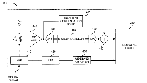
Fig. 4 is an exemplary diagram of a portion of signal conditioning logic 330
according to an implementation
consistent with the principles of the invention. In one implementation, the
portion of signal conditioning logic 330
shown in Fig. 4 is a receiver portion. Signal conditioning logic 330 may
include O/E converter 410, low pass filter
(LPF) 420, wideband amplifier 430, operational amplifier (op amp) 440, analog-
to-digital (A/D) converter 450,
microprocessor 460, digital-to-analog (D/A) converter 470, transient
compensation circuit 480, and summer 490.
O/E converter 410 may include a photodiode or the like that converts a
received optical signal into an
electrical signal. In one implementation consistent with the principles of the
invention, O/E converter 320 (Fig. 3)
includes, or is the same as, O/E converter 410. Low pass filter 420 may filter
the electrical signals output from O/E
converter 410 to allow signals under a certain frequency to pass. Wideband
amplifier 430 may amplify the signals
from low pass filter 420 and provide the amplified signals to demultiplexing
logic 340. In one implementation
consistent with the principles of the invention, the signals output by
wideband amplifier 430 include data signals with
embedded clock signals.
O/E converter 410, in operation, draws power from a power voltage VPD.
Amplifier 440 may monitor the
amount of current that is drawn from the power voltage VPD, which is
proportional to the amount of optical power that
is incident on O/E converter 410. During normal operation, this power may
remain relatively constant. When a
transient occurs, however, the power may rapidly increase or decrease for a
period of time. Amplifier 440 may detect
this power fluctuation by monitoring the voltage across a resistor (R) 445. In
an implementation consistent with the
present invention, resistor 445 may have a value of 500 92. A/D converter 450
may convert the analog signal from
amplifier 440 to a digital signal for use by microprocessor 460.
4
CA 02482803 2004-10-15
WO 03/090383 PCT/US03/11917
Microprocessor 460 may be physically located within signal conditioning logic
330 or elsewhere.
Microprocessor 460 may generate a dynamic (steady-state) threshold value,
based on the digital signal from A/D
converter 450, that compensates for long term changes in the signal power.
Microprocessor 460 monitors long term
changes in the signal power and then adjusts the threshold value to
compensate. Transients result in short term
changes in the signal power, which may not be adequately compensated for by
microprocessor 460. D/A converter
470 may convert the digital signal (e.g., threshold value) from microprocessor
460 back into an analog signal for
transmission to summer 490.
Transient compensation logic 480 compensates for signal transients for which
microprocessor 460 does not
compensate. Fig. 5 is an exemplary diagram of transient compensation logic 480
according to an implementation
consistent with the principles of the invention. Transient compensation logic
480 may include capacitor 510, resistor
520, operational amplifier (op amp) 530, resistor 540, and capacitor 550.
Operational amplifier 530 may include a
conventional operational amplifier that receives a signal from amplifier 440
(Fig. 4) and provides an output signal to
summer 490.
Capacitor 510 may connect in series with resistor 520 to the inverting input
of operational amplifier 530. In
one implementation consistent with the principles of the invention, capacitor
510 may include a 3.2 nF capacitor and
resistor 520 may include a 1 kS) resistor. Resistor 540 and capacitor 550 may
connect in parallel between the inverting
input and the output of operational amplifier 530. In one implementation
consistent with the principles of the
invention, resistor 540 may include a I k) resistor and capacitor 550 may
include a 16 pF capacitor.
These components of transient compensation logic 480 use the output of
amplifier 440 to generate a
compensation signal. If no transient exists, the compensation signal has a
zero value.
Returning to Fig. 4, the compensation signal from transient compensation logic
480 is combined with the
dynamic threshold value from microprocessor 460 by summer 490. Summer 490 may
include conventional
mechanisms to generate a threshold signal by combining the threshold value
from microprocessor 460 and the
compensation signal from transient compensation logic 480. When no transient
is present, the output of transient
compensation logic 480 is zero. When a transient exists, however, the
compensation signal from transient
compensation logic 480 is added to the dynamic threshold value from
microprocessor 460 and provided to
demultiplexing logic 340.
Demultiplexing logic 340 may use the threshold signal from summer 490 in
analyzing the signal received
from wideband amplifier 430. For example, in an implementation consistent with
the present invention,
demultiplexing logic 340 uses the threshold signal to determine the
characteristics of the signal received from
wideband amplifier 430. For example, demultiplexing logic 340 may determine
whether the signal is a one or a zero.
Fig. 6 is an exemplary diagram of demultiplexing logic 340 according to an
implementation consistent with
the principles of the invention. Demultiplexing logic 340 may include
flip/flop (F/F) 610, clock recovery logic 620,
phase shifter 630, demultiplexer 640, and forward error correction (FEC) logic
650. Phase shifter 630 and forward
error correction logic 650 have been illustrated using dotted lines. This
means that these components may be
eliminated or located somewhere other than in demultiplexing logic 340 in
other implementations consistent with the
principles of the invention.
5
CA 02482803 2004-10-15
WO 03/090383 PCT/US03/11917
Flip/flop 610 may include a D flip/flop with threshold (VTH), D, T5, and clock
(CLK) inputs and Q and Q
outputs. The threshold input may receive the threshold signal from summer 490.
The D input may receive the output
from wideband amplifier 430. The clock input may receive the output of phase
shifter 630 or clock recovery logic
620. The Q and Q outputs may provide the outputs of flip/flop 610 to
demultiplexer 640. Flip/flop 610 may use the
threshold input to determine the characteristics of the data received by the D
input. For example, flip/flop 610 may
use the threshold input to assist in determining whether the data received at
the D input is a one or a zero.
Clock recovery logic 620 may extract a clock signal from the signal output
from wideband amplifier 430.
Clock recovery logic 620 may use conventional techniques to extract the clock
signal. Phase shifter 630 may receive
an input ("phase adjust") that permits the phase of the clock signal extracted
by clock recovery logic 620 to be
adjusted. Such a phase adjustment permits the point at which the data signal
is sampled with respect to time to be
varied.
Demultiplexer 640 may include a conventional demultiplexer that receives the Q
and Q outputs from
flip/flop 610 and separates the data signals for transmission on an output bus
to FEC logic 650. FEC logic 650 may
provide forward error correction on the data signals from demultiplexer 640.
FEC logic 650 may use conventional
techniques to perform the forward error correction.
SYSTEM PROCESSING
Fig. 7 is a flowchart of exemplary processing by signal conditioning logic 330
according to an
implementation consistent with the present invention. Processing may begin
with a transient occurring due to a
relatively rapid change in power. For example, a transient may occur due to
instantaneous signal power changes
resulting from the addition or removal of one or more individual optical
channels. The characteristics (e.g., frequency
and duration) of the transient may vary based on factors, such as the physics
of the signal amplifiers and the number
and distance between the amplifiers.
Figs. 8A and 8B are graphs depicting the effects of transients on power levels
in the optical domain. Such
power levels may occur at the input of O/E converter 410. Fig. 8A illustrates
the effects of a transient resulting from a
relatively rapid increase in power. As shown in Fig. 8A, the power level
remains relatively constant (at PLO) until the
occurrence of the transient (at TO). At this point, the power level increases
(to PLI) for the duration of the transient
(until Ti) and then returns to its initial power level (at PLO). Fig. 8B
illustrates the effects of a transient resulting from
a relatively rapid decrease in power. As shown in Fig. 8B, the power level
remains relatively constant (at PLO) until
the occurrence of the transient (at TO). At this point, the power level
decreases (to PLI) for the duration of the
transient (until T1) and then returns to its initial power level (at PLO).
Returning to Fig. 7, amplifier 440 detects fluctuations in the optical power
incident upon O/E converter 410,
due, for example, to the occurrence of a power transient, by monitoring
changes in the voltage across resistor 445 (act
710). A/D converter 450 converts the output from amplifier 440 to a digital
signal and provides it to microprocessor
460. From this signal, microprocessor 460 generates and/or adjusts a dynamic
threshold value. Microprocessor 460
provides the threshold value to D/A converter 470, which converts it to an
analog signal and provides it to summer
490.
6
CA 02482803 2004-10-15
WO 03/090383 PCT/US03/11917
Transient compensation logic 480 also receives the output from amplifier 440
and generates a compensation
signal that compensates for the presence of the power transient (act 720).
When no transient is present, the
compensation signal has a value of zero. Transient compensation logic 480
provides the compensation signal to
summer 490, which combines it with the dynamic threshold value from
microprocessor 460 to generate a threshold
signal (act 730). Summer 490 provides the threshold signal to the threshold
input (VTH) of flip/flop 610 (Fig. 6) of
demultiplexing logic 340 (act 740).
Meanwhile, O/E converter 410 converts the received optical signal to an
electrical signal. Low pass filter 420
filters the electrical signal. Wideband amplifier 430 amplifies the filtered
signal and provides its output to
demultiplexing logic 340. As described above, the output of wideband amplifier
430 is a data signal with an
embedded clock signal. Wideband amplifier 430 provides the data signal to the
D input of flip/flop 610 (Fig. 6) of
demultiplexing logic 340.
Fig. 9 is a graph of possible signals input to demultiplexing logic 340. As
shown in Fig. 9, the data signal
from wideband amplifier 430 begins at a constant level and spikes upward when
the transient occurs (assuming the
transient involves an increase in power). Once the transient ends, the data
signal spikes downward and returns to the
constant level.
The threshold signal output from summer 490 is also shown in Fig. 9. The
threshold signal tracks the changes
in the data signal. In other words, the threshold signal begins at a constant
level, spikes upward when the transient
occurs, spikes downward at the end of the transient, and then returns to the
constant level. The transient compensation
logic 480 makes this tracking possible.
EXEMPLARY RESULTS
Figs. IOA and I OB are graphs that illustrate how the bit error rate (BER) is
affected by transients. Assume
for purposes of this example, that the transient occurs at time 0 and ends at
time 100. Fig. IOA illustrates the case
where signal conditioning logic 330 includes no transient compensation logic
480. As shown in Fig. 10A, the bit error
rate increases at the start and end of the transient. Fig. IOB illustrates the
case where signal conditioning logic 330
includes transient compensation logic 480. As shown in Fig. I OB, the bit
error rate remains relatively constant despite
the occurrence of the transient.
CONCLUSION
Systems and methods, consistent with the present invention, compensate for the
occurrence of power
transients. The systems and methods alter a threshold value used by
demultiplexing logic to track the increase or
decrease in power caused by the transient.
The foregoing description of exemplary embodiments of the present invention
provides illustration and
description, but is not intended to be exhaustive or to limit the invention to
the precise form disclosed. Modifications
and variations are possible in light of the above teachings or may be acquired
from practice of the invention. For
example, certain portions of the invention have been described as "logic" that
performs one or more functions. This
logic may include hardware, such as analog or digital circuitry or an
application specific integrated circuit, software, or
a combination of hardware and software.
7
CA 02482803 2004-10-15
WO 03/090383 PCT/US03/11917
No element, act, or instruction used in the description of the present
application should be construed as
critical or essential to the invention unless explicitly described as such.
Also, as used herein, the article "a" is intended
to include one or more items. Where only one item is intended, the term "one"
or similar language is used. The scope
of the invention is defined by the claims and their equivalents.
8