Note: Descriptions are shown in the official language in which they were submitted.
CA 02482976 2004-10-19
WO 03/090335 PCT/EP03/03826
Circuit arrangement with power factor correction, and
corresponding appliance
The present invention relates to a circuit arrangement
having a switch-mode power supply as claimed in the
preamble clause of claim 1, and on an appliance having
a corresponding circuit arrangement.
Switch-mode power supplies produce a~ heavily pulsed
load on the electrical power supply system, which leads
to harmonic currents in electrical power supply
systems. This load occurs in the region of the voltage
maxima of the sinusoidal mains voltage, at which
voltage maxima an energy-storage capacitor for the
switch-mode power supply is recharged. Appliances
having a relatively high power consumption, such as
televisions with relatively large picture tubes, now
therefore have to comply with specific regulations
relating to harmonic currents. The harmonic load on the
electrical power supply system caused by an appliance
can in this case be stated as a so-called power factor.
Widely differing circuit concepts are known for
improving the power factor, for example from
DE-A-196 10 762, EP-A-0 700 145 and US 5,986,898. These
contain a second current path with a coil between the
mains rectifier and the primary winding of the
transformer, with the inductance of this coil acting
like a current pump, which is controlled by a switching
transistor in the switch-mode power supply and in
consequence broadens the pulsed current flow of the
switch-mode power supply.
A further possible way to improve the power factor of a
switch-mode power supply is to use a coil in the input
area of the switch-mode power supply. This coil is also
referred to as a 50 Hz coil, a mains frequency coil or
a power factor coil. In order to avoid confusion with
CA 02482976 2004-10-19
WO 03/090335 PCT/EP03/03826
- 2 -
other coils, the description therefore always uses the
expression power factor coil for this coil.
However, this power factor coil has the disadvantage
that the current flow in the power factor coil is
interrupted suddenly when the mains switch is operated
in order to switch off the appliance. The energy which
is stored in the coil must be dissipated, however.
Since the open mains switch represents the highest
impedance in the circuit, a very high voltage is
therefore developed across the switching contacts of
the mains switch, and causes an arc. This causes the
mains switch to age more quickly, and the switch
represents a safety risk since, in the worst case, it
becomes a potential fire source.
Other mains switches, in which the switching contacts
open at a slow rate, are likewise at risk. In this
case, although the voltage across the contacts is not
very high, an arc is nevertheless produced, however,
and burns until the end of the corresponding power
supply system half-cycle. In this case as well, a large
amount of energy is lost in the switch, which leads to
rapid aging.
The object of the present invention is to specify a
circuit arrangement and a corresponding appliance of
the type mentioned initially, which have a high
reliability, combined with a low circuit complexity.
For a circuit arrangement, this object is achieved by
the features of claims 1, 7 and 8, and for an appliance
it is achieved by the features of claim 9. Advantageous
developments of the invention are specified in the
dependent claims.
The circuit arrangement according to the invention has
a mains connection, a mains switch with two switching
CA 02482976 2004-10-19
WO 03/090335 PCT/EP03/03826
- 3 -
contacts, a demagnetization coil and a switch-mode
power supply, which comprises a driver circuit for
producing a control voltage for the switching
transistor of the switch-mode power supply. A first
switching contact of the mains switch is arranged here
between the mains connection and the demagnetization
coil in order to switch the demagnetization coil on and
off, and the second switching contact is connected to a
supply or control voltage for the driver circuit, in
order to switch off the control voltage for the
switching transistor or in order to switch off the
switch-mode power supply.
This has the advantage that a power factor coil between
the mains connection and the switch-mode power supply
can be used for power factor correction, and that the
mains switch is not loaded by the inductance of the
power factor coil. Admittedly, this results in the
switch-mode power supply being connected to the mains
even when it is switched off. However, this is not
disadvantageous for the user and leads only to a slight
power loss resulting from the starting circuit, when
the switch-mode power supply is switched off.
The circuit arrangement can be used in particular' in
appliances having a picture tube, for example
televisions and computer monitors. This mains switch
circuitry in this case ensures that the picture tube is
demagnetized whenever the appliance is switched on.
The invention will be explained in more detail in the
following text using, by way of example, an exemplary
embodiment which is illustrated schematically in the
figures, in which:
Figure 1 shows a circuit arrangement having a mains
connection, a power factor coil and a switch-
CA 02482976 2004-10-19
WO 03/090335 PCT/EP03/03826
- 4 -
mode power supply, as well as a mains switch,
and
Figure 2 shows the use of the arrangement in a chassis
of a television.
Figure 1 shows a switch-mode power supply I
schematically, which has a rectifier means, in this
exemplary embodiment a bridge rectifier BR with four
diodes, an energy-storage capacitor C1 and transformer
TR with a primary winding W1, an auxiliary winding W2
arranged on the primary side and secondary windings W3,
W4 and W5 arranged on the secondary side. The energy-
storage capacitor C1 is in this case arranged between
the bridge rectifier BR and the primary winding W1. A
switching transistor T1 is connected in series with the
primary winding W1 and is controlled by a control
voltage DS for a driver circuit DC. A supply voltage
VCC is provided for operation of the switch-mode power
supply via the auxiliary winding W2, a diode D1 and
capacitor C2, and is supplied to the driver circuit DC.
The switch-mode power supply I in Figure 1 is a part of
a circuit arrangement which also has a mains connection
NA, a demagnetization coil (which is not illustrated)
and a mains switch S1 with two switching contacts 1, 2.
The circuit arrangement is preferably integrated in an
appliance, for example a television, which has a
picture tube.
Picture tubes, which are used in televisions or
computer monitors, need to be demagnetized from time to
time in order to preserve the color purity of the
picture tube. This is accomplished by means of a
demagnetization coil, through which an AC voltage
normally flows during the process of switching on the
appliance. The 220 volt mains voltage is used as the AC
voltage in this case and produces a high current surge
at the time when the appliance is switched on, and
CA 02482976 2004-10-19
WO 03/090335 PCT/EP03/03826
- 5 -
which then subsequently decays gradually. The decay is
accomplished by means of a posistor, which is heated by
the high current with its impedance in consequence
becoming high.
In order to regulate the switch-mode power supply, the
driver circuit DC is supplied with a regulating signal
RS which is derived from a supply voltage U4 on the
secondary side, for example from the system voltage in
a television, and is transmitted via an opto coupler or
an isolating transformer (which is not illustrated) to
the primary side of the switch-mode power supply.
A so-called snubber network SN is arranged in parallel
with the primary winding W1 and is used to damp voltage
spikes which occur during the process of switching off
the switching transistor T1. The switch-mode power
supply also contains a starting circuit AS, which
supplies the driver stage DC with a current for the
starting phase of the switch-mode power supply after
the appliance in which the circuit arrangement is
integrated has been switched on. The starting circuit
AS is normally a high-value resistor chain, which
produces a connection between the bridge rectifier BR
and the capacitor C2. During operation, the supply
voltage VCC is produced by the auxiliary winding W2, as
well as by the diode D1 and the filter capacitor C2.
The switch-mode power supply illustrated in the figure
preferably operates on the basis of the fly back
converter principle, although other circuit principles
are likewise possible. Fly back converters are
preferably used in entertainment electronics
appliances, for example in televisions and video
recorders. In a fly back converter, energy is in this
case stored in the transformer TR during the phase in
which the switching transistor T1 is switched on, and
is then subsequently transmitted to the windings W3-WS
CA 02482976 2004-10-19
WO 03/090335 PCT/EP03/03826
- 6 -
on the secondary side, and to the auxiliary winding W2
on the primary side, in the phase during which the
switching transistor is switched off. Fly back
converters are used both as AC/DC converters and as
DC/DC converters.
Switch-mode power supplies of this type have a low
power factor, since the energy-storage capacitor C1 is
recharged only in the region of the voltage maxima and
minima of the 50 Hz mains voltage, when the output
voltage U2 of the bridge rectifier BR exceeds the
voltage value across the energy-storage capacitor C1.
One simple possible way to improve the power factor of
a switch-mode power supply is to use a mains frequency
coil or power factor coil NS, which is arranged between
the mains connection NA and the energy-storage
capacitor C1. In this exemplary embodiment, it is
connected between the mains connection NA and the mains
rectifier BR.
The power factor coil NS results in the pulsed current
flow which is used to recharge the energy-storage
capacitor C1 being broadened and shifted in phase,
since the inductance of this coil, for example 50 mH,
means that the current flow through the coil rises only
gradually, and decays again in a damped manner. A power
factor which complies with the requirements is achieved
in this case by appropriate choice of the inductance
value.
Figure 1 likewise shows a mains switch S1, which has
two switching contacts 1 and 2, as well as
corresponding connections a and b for the switching
contact 1, and c and d for the switching contact 2. The
mains switch S1 is in this case normally arranged on
the front face of the appliance, such that it is easily
accessible for a user. The connections c and d are in
this case according to the invention connected to the
CA 02482976 2004-10-19
WO 03/090335 PCT/EP03/03826
connections c' and d' for switching the driver circuit
DC of the switch-mode power supply on and of f , and the
connections a and b are connected to the magnetization
coil for switching the demagnetization coil on and off.
In consequence, the power factor coil NS is not
arranged in the current path of the mains switch S1.
The mains switch is therefore not loaded by the power
factor coil NS when the appliance is switched on and
off. At the same time, this arrangement ensures that
the demagnetization coil is switched on, in order to
demagnetize the picture tube, on each occasion when the
appliance is switched on.
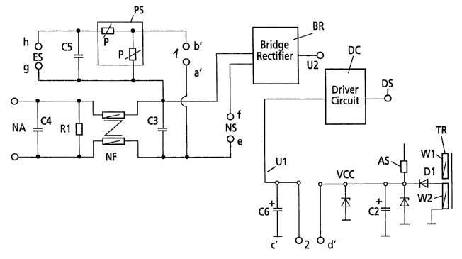
Figure 2 shows the major components of the circuit
arrangement , to the extent that they are integrated on
a chassis of a television in an advantageous
refinement. On the input side, the arrangement has a
filter section with a mains filter NF, capacitors C3
and C4 and a resistor R1, which filter section is
connected to the mains connection NA of the
arrangement. This filter section prevents radiated
interference from the appliance entering the mains
system and suppresses any interference which is already
present on the mains system. On the output side, the
filter section is connected to the bridge rectifier BR,
which provides the rectified voltage U2 for operation
of the switch-mode power supply.
Connections a and f are arranged in the connection
between the bridge rectifier and the filter section, to
which the power factor coil NS, which is not
illustrated in Figure 2, is connected. The power factor
coil is arranged separately, so that the switch-mode
power supply can be kept compact and, in particular,
such that an already existing switch-mode power supply
which does not have power factor correction can be used
without any major design change. The arrangement of the
CA 02482976 2004-10-19
WO 03/090335 PCT/EP03/03826
_ g _
power factor coil NS upstream of the bridge rectifier
BR means that it is located in the current path of the
sinusoidal AC voltage of the mains system.
The driver circuit DC and the transformer TR for the
switch-mode power supply are indicated only
schematically in Figure 2, to the extent that it is
necessary for understanding of the invention. As
already explained with reference to Figure 1, a diode
D1 and a capacitor C2 are arranged on the auxiliary
winding W2, which is arranged on the primary side, in
order to produce the operating voltage vCC for the
driver circuit. Two connection points c' and d' are
arranged on the chassis in the connection between the
capacitor C2 and the driver circuit DC, and are
connected to the connection points c and d of the mains
switch S1.
A capacitor C6 with a capacitance of 1 ~.F is also
advantageously connected to ground between the
connection c' and the driver circuit DS, and is used to
avoid switch bouncing of the switching contact 2 and to
provide filtering for the long supply line to the mains
switch S1. The capacitance of this capacitor in this
case also influences the number of switching cycles
after which the switching transistor T1 is completely
switched off.
A posistor PS and a capacitor C5 to which the
demagnetization coil ES (which is not illustrated) is
connected via connection points g and h are also
arranged on the chassis. On the input side, the
posistor PS is arranged in parallel with the capacitor
C3. Connection points a' and b', which are connected to
the connection points a and b of the mains switch S1,
are in this case located in a supply. In consequence,
the demagnetization coil ES is switched on whenever the
mains switch S1 is operated in order to switch on the
CA 02482976 2004-10-19
WO 03/090335 PCT/EP03/03826
_ g _
appliance. The posistor PS in this case ensures a large
current surge at the moment of switching on, which is
reduced continuously to a low loss level by the heating
of the posistor.
Whenever the appliance is switched, when the mains
switch S1 is pressed, the switching contacts 1 and 2
are closed, so that the switch-mode power supply can be
started via the switching contact 2, since the driver
circuit DC is in this case supplied with the operating
voltage VCC. On being switched on, the switch-mode
power supply thus behaves in precisely the same way as
when using the mains switch S1 in appliances of a
conventional type.
Whenever the appliance is switched off, when the mains
switch S1 is opened, the switching contact 2 switches
off the switching transistor T1 in a short time, so
that no more energy is transmitted in the transformer
TR to the second windings W2 - W5. The switching
voltage DS for the switching transistor T1 is switched
off directly or indirectly by the driver circuit. The
switching contact 2 is advantageously connected to the
connection points c' and d', as described with
reference to Figure 2, so that the driver circuit DC is
disconnected from the supply voltage VCC during the
switching-off process. However, another voltage of the
driver circuit DC, for example a control voltage for
the driver circuit DC, can also be switched off in a
corresponding manner by the switching contact 2, or the
switching contact 2 can be used to regulate the
regulating signal RS at a predetermined voltage level,
so that the switching transistor T1 is likewise
switched off permanently.
According to the invention, the mains connection NA is
thus connected to the bridge rectifier BR without being
switched, without a mains switch. The switch-mode power
CA 02482976 2004-10-19
WO 03/090335 PCT/EP03/03826
- 10 -
supply I is thus always connected to the electrical
power supply system whenever the mains plug of the
appliance is connected to the electrical power supply
system. In consequence, the power factor coil NS is not
arranged in the current path of the mains switch S1, so
that the life of the mains switch S1 is considerably
improved.
Further refinements of the invention are within the
scope of a person skilled in the art . The invention is
not restricted to switch-mode power supplies based on
the flyback converter principle, as already explained
above, and can also be used for other switch-mode power
supply concepts when power factor correction is
required. The invention can also be used in appliances
which do not have power factor correction. Thus, for
example, the connection points a and f can be short-
circuited in appliances for countries which do not
require power factor correction. In consequence, there
is no need to modify the chassis in these appliances
for these countries.