Note: Descriptions are shown in the official language in which they were submitted.
CA 02483237 2004-09-30
Y-K Chen 31-5-3
OPTICAL DIGITAL-TO-ANALOG CONVERTER
Technical Field
This invention relates to optical waveform generation systems and, more
particularly, to conversion of digital signals into analog optical signals.
Background of the Invention
Digital-to-analog (D/A) converters are key elements in both electronic and
photonic signal processing and data transmission. In many optical transmission
systems, digital data has to be converted to analog form for processing and/or
transmission. Indeed, there are many advantages for using optical technology
to
implementing D/A converters, for example, high-speed clocking and signal
sampling,
wide-bandwidth, light-weight components and the like. Additionally, a high-
speed
arbitrary analog waveform generator can be implemented using a very high-speed
D/A converter.
One such optical D/A converter is described in an article entitle "Digital-to-
Analog Conversion Using Electrooptic Modulators", authored by A. Yacoubian et
al.,
IEEE Photonics Technology Letters, Vol. 15, No. 1, January 2003, pages 117-
119.
However, the disclosed implementation is limited to a so-called 2-bit photonic
D/A
converter.
Summary of the Invention
These and other problems and limitations of prior known optical modulation
arrangements are overcome in applicants' unique invention by utilizing a
continuous
wave or pulsed laser optical signal, which is split into a plurality of
mutually coherent
optical beams. Each of the plurality of optical beams is phase shift modulated
by bits
(control signals) of a data sequence to generate a corresponding plurality of
phase
shift modulated mutually coherent optical signals. The modulated optical
signals are
recombined to form the desired digital-to-analog converted optical signal for
use as
desired.
In one specific embodiment of the invention, the phase modulation is effected
by splitting optical signal comprising a continuous wave laser optical signal
into a
plurality of similar mutually coherent optical signals, phase shift modulating
the
continuous wave optical coherent signal of each of the similar continuous wave
laser
CA 02483237 2006-07-14
2
optical signals with the digital data bits (control signals). Then, the
plurality of phase
shifted modulated continuous wave optical signals are combined to yield the
resulting
converted digital-to-analog signal.
In another embodiment of the invention, the supplied digital data sequence is
preprocessed via a processor before the data bits of the sequence are supplied
to
modulate the plurality of mutually coherent versions of the supplied
continuous wave
laser optical signal.
In yet another embodiment of the invention, a pulsed laser signal is supplied
as
an input to the optical digital-to-analog converter. The pulsed laser optical
signal is split
into a plurality of mutually coherent optical beams, which are phase shift
modulated by
data sequences stored in a memory to generate a substantially jitter free
analog optical
signal after the phase shift modulated optical beams are recombined. The
pulsed laser
optical signal is controlled to have the same repetition rate as the data
sequence from
the memory unit. By properly aligning the data sequence with the pulses of the
pulsed
laser optical signal, the effect of timing jitter is canceled.
In still another embodiment of the invention, instead of stacking more phase
shift modulators in a single stage digital-to-analog converter, a plurality of
digital-to-
analog converter stages having fewer phase shift modulators are cascaded to
form the
overall digital-to-analog converter, in accordance with the invention. This
embodiment
of the invention is advantageous to realize a desired distribution of discrete
output
levels.
In an exemplary embodiment, the present invention provides a method of
optically converting a digital signal to an analog signal, by employing a
conversion
module, comprising the steps of: receiving a predetermined optical signal;
splitting the
received optical signal into a plurality of mutually coherent optical beams;
supplying
said plurality of optical beams on a one-to-one basis to a corresponding
plurality of
optical phase shifters; supplying bits of a digital data sequence to said
plurality of
optical phase shifters for controlling the phase shift of the optical beams
supplied to the
individual ones of said plurality of phase shifters; supplying said phase
shifted optical
beams to a combiner for recombining mutually coherent phase shifted optical
beams;
and said combined mutually coherent phase shifted optical beams representing
an
optically converted digital-to-analog optical signal.
CA 02483237 2006-07-14
2a
Brief Description of the Drawings
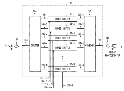
FIG. 1 shows, in simplified block diagram form, one embodiment of the
invention;
FIG. 2 also shows, in simplified block diagram form, a second embodiment of
the invention;
FIG. 3 illustrates, in simplified block diagram form, a third embodiment of
the
invention; and
CA 02483237 2004-09-30
Y-K Chen 31-5-3 3
FIG. 4 shows, in simplified block diagram form, details of a fourth
embodiment of the invention.
Detailed Description of Embodiments of the Invention
FIG. 1 shows, in simplified block diagram form, one embodiment of the
invention. Specifically, shown is optical light source 101 typically including
a
continuous wave or pulsed laser to generate an optical signal at a desired
wavelength.
Exemplary optical signals to be processed have optical frequencies of about
2.3x10¹⁴
Hertz to about 1.8x10¹⁴ Hertz, i.e., a wavelength of about 1.3 microns to
about 1.7
microns. In one example, a continuous wave optical signal having a wavelength
of
approximately 1.55 microns, i.e., a frequency of 1.93 x10¹⁴ Hertz, is
generated by
light source 101 and supplied via 102 to optical digital-to-analog converter
100. In
optical digital-to-analog converter 100 the continuous wave optical signal is
supplied
via optical path 103 to splitter 104, which generates a plurality of N
mutually coherent
optical beams 105-1 through 105-N. The number N of the mutually coherent beams
has to be at least two (2), but four (4) to eight (8) optical beams are
typically
employed. The importance of the plurality N of optical beams being mutually
coherent in this application will be discussed below. In this example,
splitter 104 is a
multimode interference (MMI) coupler. The plurality N of mutually coherent
optical
beams are supplied on a one-to-one basis to a corresponding plurality of
optical phase
shifters 106-1 through 106-N, respectively. . Also supplied via 112-1 through
112-N
to phase shifters 106-1 through 106-N are bits, i.e., control signals, of a
data sequence
for causing the phase shifts in phase shifters 106-1 through 106-N to effect
the desired
digital-to-analog conversion. Thus, in this example, the digital-to-analog
conversion is
realized by use of an electro-optical phase shift modulation scheme through
either
direct phase shift modulation of the continuous wave optical beams from laser
101 or
by an external phase shift modulation using, for example, a Mach Zehnder phase
shift
modulator. The frequency of the modulation signal is in the
microwave/millimeter-
wave range. The phase shift modulated outputs from phase shifters 106-1
through
106-N are supplied via optical paths 107-1 through 107-N, respectively, to
optical
combiner 108, where they are recombined to form the desired optical analog
signal. In
CA 02483237 2004-09-30
Y-K Chen 31-5-3 4
this example, combiner 108 is a multimode interference (MMI) coupler. This
analog
optical signal is supplied via optical paths 109 and 110 to linear photodiode
111,
which yields an electrical signal for use as desired.
The recombined phase shift modulated optical signal being detected by
photodiode 111 developes current ipõ through photodiode 111 which is
calculated as
follows:
2
i po = RP,,, exp jTr V
V"
where R is the responsivity of photodiode 111, P.,, the launched optical
power, V,. the
control voltage for the i-th phase shift modulator and V,, the switching
voltage for a
1 o phase shift -modulator. If the control voltages are now configured such
that each of
them can have two different levels, namely, V,,,,, and V,,i , 2' output
current ipD levels
are realizable. If the two different control voltage levels V r~w and V Mi are
switched
between at a "high" rate an arbitrary waveform is developed at the output of
photodiode I l 1. The so-called "high" rate is typically 10-40 Gbits/s, but
could be as
high as 160 Gbits/s.
The phase shift modulator 106 of each branch can be fabricated e.g. in a
material system with linear electro-optic effect, as InP, GaAs or LiNbO3. The
effective refractive index of an optical waveguide changes in proportion to
the applied
electrical field perpendicular to this waveguide. A high frequency distributed
electrical waveguide is engineered to co-propagate with the optical wave with
matched propagating velocity to deliver the local electrical field with high
modulation
bandwidth. The different branches will delay the optical signal by a different
length
of time. This results in different phases at the outputs of phase shifters
106. In the
combiner 108, these different output phase signals that interfere
constructively have a
different optical signal phase due to the different time delays these signals
experienced. The resulting optical signal after the MMI coupler, i.e.,
combiner 108, is
the sum of all the phase shifted optical signals that interfere
constructively.
CA 02483237 2004-09-30
Y-K Chen 31-5-3 5
FIG. 2 also shows, in simplified block diagram form, a second embodiment of
the invention. The embodiment of FIG. 2 is similar to that of FIG. I and
includes
similar elements that are essentially identical from both a physical and
functional
standpoint. These similar elements have been similarly numbers as those in
FIG. 1
and will not be discussed again in detail. The only significant difference
between the
embodiments of FIG. 1 and FIG. 2 is the use of processor 201. As can be seen,
one or
more data signals are supplied to processor 201 via input connection 202. In
processor 201, the data signals are employed to code and generate control
voltage
signals for driving, phase shift modulators 106-1 through 106-N. These
coritrol
voltage signals are supplied via output connections 112-1 through 107-N to
phase
shifters 106-1 through 106-N, respectively.
FIG. 3 illustrates, in simplified block diagram form, a third embodiment of
the
invention. The embodiment of FIG. 3 is also similar to that of FIG. 1 and
includes
similar elements that are essentially identical from both a physical and
functional
standpoint. These similar elements have been similarly numbers as those in
FIG. I
and will not be discussed again in detail. The only significant difference
between the
embodiments of FIG. 1 and FIG. 3 is that a pulsed laser signal is supplied as
an input
from pulsed laser 301 to the optical digital-to-analog converter 100, and that
the
pulsed laser optical signal 102 is controlled to have the same repetition rate
as the data
sequence from memory unit 302. The pulsed laser optical signal is split into a
plurality of mutually coherent optical beams 105-1 through 105-N via splitter
104,
which are phase shift modulated via phase shifters 106-1 through 106-N by data
sequences stored in a memory to generate a substantially jitter free analog
optical
signal after the phase shift modulated optical beams are recombined. The
pulsed laser
optical signal 102 is controlled via clock 303 to have the same repetition
rate as the
data sequence from memory unit 302. By properly aligning the data sequence
with
the pulses of the pulsed laser optical signal, the effect of timing jitter is
canceled.
FIG. 4 shows, in simplified block diagram form, details of another digital-to-
analog converter 100 in accordance with the invention. In this embodiment a
plurality
of digital-to-analog converter stages 100-1 through 100-J are cascaded in
order to
CA 02483237 2004-09-30
Y-K Chen 31-5-3 6
realize a desired number of phase shift modulated optical beams in obtaining
the
overall digital-to-analog conversion. As noted above at least two (2) branches
are
required in each stage with an overall number of stages being two (2) to four
(4), i.e.,
between four (4) and eight (8) branches of optical beams to be phase shift
modulated
by the bits of the data sequence, i.e., the control voltage signals. This
analog optical
signal is supplied via optical paths 109 and 110 to linear photodiode 111,
which yields
an electrical signal for use as desired. This embodiment is advantageous to
realize a
desired distribution of discrete output levels.
The recombined phase shift modulated optical signal being detected by
photodiode 111 developes current iPD through photodiode 111, which is
calculated as
follows:
~I . 2
iYD = RPn, fl Y exp j7r
;
wherej is the running index for the j-th stage.
The above-described embodiments are, of course, merely illustrative of the
principles of the invention. Indeed, numerous other methods or apparatus may
be
devised by those skilled in the art without departing from the spirit and
scope of the
invention.