Note: Descriptions are shown in the official language in which they were submitted.
CA 02483731 2007-11-02
TECHNICAL FIELD
The present invention relates to an optical disk.
BACKGROUND ART
Recently, optical disks having various structures with enhanced features and
dramatically
increased storage capacities have been developed to improve, among other
things, their recording
density. The currently-used high density optical disks include DVD-R, DVD-RAM,
and the like.
Figure 1 and Figure 2 illustrate diagrams of a high-density optical disk
according to a related art
and the dimensions of various elements. These figures show a disk 20 having a
thickness of 1
mm and a diameter of 120 mm. A via hole 22 is formed at a central portion of
the disk 20. The
disk 20 has an outer recording layer 10 and a central portion 24 of the disk
20 having the via hole
22. A diameter of the via hole is about 15 mm, and a diameter of the central
portion is about 44
mm. The recording layer 10 is formed at a location about 0.1 mm from a surface
of the disk 20
on which light is incident.
In the illustrated disk, a protecting layer 30 is formed on the recording
layer 10 to protect the
recording layer 10. The protecting layer 30 is formed by attaching a
transparent plastic film, such
as a polycarbonate sheet, to the recording layer 10 or spin-coating a UV-
hardening resin on the
recording layer 10.
The process of spin-coating on the protecting layer 30 is explained as
follows.
First, a UV-hardening resin in a liquid state is dropped on the recording
layer 10 adjacent to the
central portion 24 of the disk 20. The disk 20 is then rotated at a
predetermined spin speed
based, in part, on the viscosity of the resin. The spinning disk causes the UV-
hardening resin to
spread across the recording layer 10 from the central portion to the
circumference in response to
centrifugal force. Once the resin spreads across the surface of the recording
layer 10, the UV-
hardening resin coated on the disk is hardened by exposing the resin to UV
rays.
-1-
CA 02483731 2007-11-02
However, spin-coating fails to evenly distribute the UV-hardening resin across
the recording
layer 10 in creating a protecting layer of a uniform thickness. Instead, as
illustrated in Figure 1,
the thickness of the UV-hardening resin formed on the recording layer 10
becomes thicker as the
protecting layer 10 approaches the outer circumference of the disk 20.
Hence, thickness deviations in the protecting layer 30 interfere with the
recording/reading of
information on/from the recording layer 10.
DISCLOSURE OF INVENTION
Accordingly, the present invention is directed to an optical disk that
substantially obviates one or
more problems due to limitations and disadvantages of the related art.
An object of the present invention is to provide an optical disk enabling with
a protecting layer
having a uniform thickness thereon.
Additional advantages, objects and features of the invention will be set forth
in part in the
description which follows and in part will become apparent to those having
ordinary skill in the
art upon examination of the following or may be learned from practice of the
invention. The
objectives and other advantages of the invention may be realized and attained
by the structure
particularly pointed out in the written description and claims hereof as well
as the appended
drawings.
To achieve these objects and other advantages and in accordance with the
purpose of the
invention, as embodied and broadly described herein, an optical disk according
to the present
invention includes a plate having a first area enabling to record information
thereon and a second
area unable to record the information thereon and a projection on the second
area of the plate.
The optical disk, according to one embodiment of the invention, includes a
first area for
-2-
CA 02483731 2007-11-02
recording information thereon, the first area having an outer circumferential
edge, an inner
circumferential edge and an upper surface; a second area located within the
inner circumferential
edge of the first area; and, a projection, located within the second area,
that vertically extends
beyond the upper surface of the first area which prevents full contact with
the upper surface of
first area when engaging a supporting surface.
It is to be understood that both the foregoing general description and the
following detailed
description of the present invention are exemplary and explanatory and are
intended to provide
further explanation of the invention as claimed.
BRIEF DESCRIPTION OF THE DRAWINGS
The accompanying drawings, which are included to provide a further
understanding of the
invention and are incorporated in and constitute a part of this application,
illustrate
embodiment(s) of the invention and together with the description serve to
explain the principle of
the invention.
In the drawings:
Figure 1 and Figure 2 illustrate diagrams of a high-density optical disk
according to a related art;
Figure 3 illustrates a diagram of a thickness of a protecting layer formed by
spin-coating;
Figures 4 to 6 illustrate cross-sectional views of optical disks according to
embodiments of the
present invention;
Figure 7A and Figure 7B illustrate cross-sectional views of a process of
forming a protecting
layer of an optical disk according to the present invention; and
Figure 8 illustrates a diagram for protecting a disk surface by a projection
of an optical disk
-3-
CA 02483731 2007-11-02
according to the present invention.
BEST MODE FOR CARRYING OUT THE INVENTION
Reference will now be made in detail to the preferred embodiments of the
present invention,
examples of which are illustrated in the accompanying drawings. Wherever
possible, the same
reference numbers will be used throughout the drawings to refer to the same or
like parts.
Figures 4 to 6 illustrate cross-sectional views of optical disks according to
preferred
embodiments of the present invention that include various configurations of a
projection that
facilitates fabrication of the protecting layer and provides protection for
the recording surface of
the disk once formed.
These figures illustrate an optical disk 45 according to the present invention
that includes a first
area for recording information thereon and a second area that is not used to
record information.
The first area extends to the circumferential edge of the optical disk. In
each of the various
embodiments, the first area includes a recording layer 50 that is covered by a
protecting layer 60.
Both of the recording and protecting layers are supported on a substrate or
plate 40.
The second area is located inside the first area of the optical disk in a
central portion 80 of the
plate 40. In contrast with the first area, neither the protecting layer 50 nor
the recording layer 60
extends into the second area. The second area is non-recordable. As reflected
in each of the
figures, the second area also includes a via hole formed in the central
portion 80 of the plate 40
near the rotational center of the optical disk 45.
The second area of the optical disk 20 also includes a projection 70 formed
near the
circumferential outer edge of the central portion 80. The projection is formed
to accomplish at
least two functions. As explained later, the structure of the projection
facilitates fabrication of
-4-
CA 02483731 2007-11-02
the optical disk by preventing material for collecting in the central portion
of the disk, such as
during the processing of spinning resin to form a protecting layer.
Additionally, the projection serves the function of protecting the recording
surface of the disk
from scratches and other damages. Each embodiment of the projection is
designed to prevent
full impact of the disk when engaging a supporting surface, such as the
ground.
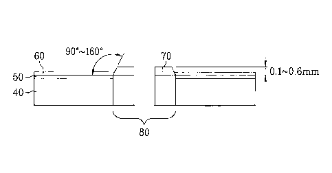
Figure 4 illustrates a first preferred embodiment of an optical disk with the
projection. There, the
projection 70 is formed to have at least one lateral side, which is inclined.
A flank angle of the
projection 70 is preferably formed to be about 90.about.160°. The flank
angle of the
projection 70 is defined as the angle formed between the upper surface of the
recording layer 10
and the lateral side of the projection 70 where the vertex of the angle is
located at the intersection
of the inner circumferential edge of the upper surface of recording layer 50
with the control
portion 80. The upper surface of the projection 70 is formed to be higher than
the upper surface
of the protecting layer 60. For example, when the optical disk has a thickness
of 1.2 mm, a
diameter of 120 mm, a diameter of the via hole of about 15 mm, and a diameter
of the central
portion of about 44 mm, a height of the projection 70 is preferably about
0.1.aboutØ6 mm.
Figure 5 shows a second preferred embodiment of the optical disk 20 where the
projection 70 is
similar to the embodiment shown in Figure 4 except the projection 70 includes
a second lateral
side formed on an inner lateral wall of the projection that is also angled. In
a related example,
the flank angle of the inner lateral projection wall is equal to the flank
angle of the outer lateral
projection wall. In this embodiment, the flank angle of the inner wall is
measured between the
upper surface of the central portion and the inner lateral projection wall.
Figure 6 shows a third preferred embodiment of an optical disk having a
projection that is similar
to the preferred embodiment of Figure 4 except the base of the outer
projection wall is offset
from the protecting layer 50. In one example, the vertex of the flank angle
occurs nearer the
center of the optical disk. One side of the flank angle is defined by the
upper surface of the
central portion 80 that is parallel to the upper surface of the protecting
layer 50.
-5-
CA 02483731 2007-11-02
,
,
'
A process for fabricating an optical disk in accordance with a preferred
embodiment of the
invention having the step of spin-coating a material for forming the
protecting layer 60 on the
disk having the projection 70 thereon is explained as follows.
Figure 7A and Figure 7B illustrate cross-sectionalal views of the constituent
elements of an
optical disk formed by a process according to the present invention.
Referring to Figure 7A, a liquefied UV-hardening resin 60 is dropped on a
recording layer 50
near the projection 70.
Referring to Figure 7B, the optical disk is spun causing centrifugal force to
move the UV-
hardening resin coated on the disk from the center portion toward the outer
circumferential edge
of the first area. The coated UV-hardening resin is then hardened by UV light.
When the step of spin-coating is carried out on the UV-hardening resin, the
projection 70 having
an inclined lateral side prevents the liquefied UV-hardening resin from
flowing into and
collecting within the central portion of the disk.
Moreover, the projection 70 maintains a uniform flow of the liquefied UV-
hardening resin during
spin-coating, thereby enabling the process to form a protecting layer 60 that
is uniform in
thickness.
INDUSTRIAL APPLICABILITY
The present invention provides an optical disk enabling to form a protecting
layer having a
uniform thickness and also provides an optical disk enabling to facilitate a
fabricating process
thereof.
It will be apparent to those skilled in the art that various modifications and
variations can be
-6-
CA 02483731 2007-11-02
=
made in the present invention. Thus, it is intended that the present invention
covers the
modifications and variations of this invention provided they come within the
scope of the
appended claims and their equivalents.
-7-