Sélection de la langue

Search

Sommaire du brevet 2483731 

Énoncé de désistement de responsabilité concernant l'information provenant de tiers

Une partie des informations de ce site Web a été fournie par des sources externes. Le gouvernement du Canada n'assume aucune responsabilité concernant la précision, l'actualité ou la fiabilité des informations fournies par les sources externes. Les utilisateurs qui désirent employer cette information devraient consulter directement la source des informations. Le contenu fourni par les sources externes n'est pas assujetti aux exigences sur les langues officielles, la protection des renseignements personnels et l'accessibilité.

Disponibilité de l'Abrégé et des Revendications

L'apparition de différences dans le texte et l'image des Revendications et de l'Abrégé dépend du moment auquel le document est publié. Les textes des Revendications et de l'Abrégé sont affichés :

  • lorsque la demande peut être examinée par le public;
  • lorsque le brevet est émis (délivrance).
(12) Brevet: (11) CA 2483731
(54) Titre français: DISQUE OPTIQUE
(54) Titre anglais: OPTICAL DISK
Statut: Périmé et au-delà du délai pour l’annulation
Données bibliographiques
(51) Classification internationale des brevets (CIB):
  • G11B 07/24027 (2013.01)
(72) Inventeurs :
  • LEE, SEOUNG-WON (Republique de Corée)
  • SEO, HUN (Republique de Corée)
  • LEE, JUN-SEOK (Republique de Corée)
  • KIM, JIN-HONG (Republique de Corée)
  • PARK, KYUNG-CHAN (Republique de Corée)
(73) Titulaires :
  • LG ELECTRONICS INC.
(71) Demandeurs :
  • LG ELECTRONICS INC. (Republique de Corée)
(74) Agent: MOFFAT & CO.
(74) Co-agent:
(45) Délivré: 2015-06-30
(86) Date de dépôt PCT: 2003-04-17
(87) Mise à la disponibilité du public: 2004-03-25
Requête d'examen: 2007-11-02
Licence disponible: S.O.
Cédé au domaine public: S.O.
(25) Langue des documents déposés: Anglais

Traité de coopération en matière de brevets (PCT): Oui
(86) Numéro de la demande PCT: PCT/KR2003/000787
(87) Numéro de publication internationale PCT: KR2003000787
(85) Entrée nationale: 2004-10-15

(30) Données de priorité de la demande:
Numéro de la demande Pays / territoire Date
10-2002-0054603 (Republique de Corée) 2002-09-10

Abrégés

Abrégé français

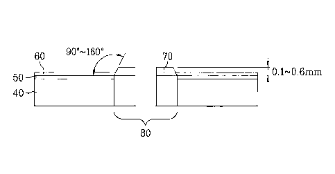
L'invention concerne un disque optique qui comporte une première zone, sur laquelle des informations peuvent être enregistrées, et une seconde zone, sur laquelle les informations ne peuvent pas être enregistrées, ladite seconde zone présentant une saillie. Selon l'invention, il est possible de former sur ce disque optique une couche protectrice d'une épaisseur uniforme.


Abrégé anglais


The present invention is directed to an optical disk having a projection that
prevents full contact
of the upper surface of the disk when engaging a supporting surface. The
optical disk includes a
projection formed in a central portion of the optical disk that abuts or is
near the upper surface of
a protecting layer.

Revendications

Note : Les revendications sont présentées dans la langue officielle dans laquelle elles ont été soumises.


WHAT IS CLAIMED:
1. An optical disk comprising:
a first side being recordable and a second side opposite the first side being
non-
recordable;
a recordable first area and a non-recordable second area, each of which is
located
between the first and second sides, respectively;
a recording layer located about 0.1 mm below a surface of the first side; and
a projection extending from the first side on the non-recordable second area
and around
a center hole;
wherein the projection is formed on a first portion of the non-recordable
second area,
the first portion being located at a diameter of larger than 15mm and nearer
the center hole
than the recordable first area, a second portion being on the first side of
the non-recordable
second area on which the projection is not formed; and
wherein the projection has at least one inclined lateral side, an upper side
and a bottom
side, a width of the upper side being smaller than that of the bottom side,
the inclined lateral
side being gradually inclined from an end of the upper side to an end of the
bottom side, and
wherein the projection is configured to prevent the first side from direct
contact with a
surface on which the optical disk is placed.
2. The optical disk of claim 1, wherein a flank angle of the projection is
greater than 90
degrees and less than 160 degrees.
3. The optical disk of claim 1 or 2, wherein an upper surface of the
projection is higher
than that of the recordable first area.
4. The optical disk of any one of claims 1 to 3, wherein a height, h, of the
projection
above the recording layer is in a range as follows, (about 0.1 mm)<h<(about
0.6 mm).
5. The optical disk of any one of claims 1 to 4, the recordable first area
comprising:
-8-

a recording layer to record the information thereon; and
a protecting layer on the recording layer to protect the recording layer.
6. The optical disk of claim 1, wherein the recordable first area and non-
recordable
second area are located on circumferential and central portions of a plate,
respectively.
7. The optical disk of any one of claims 1 to 6, wherein the non-recordable
second area
has an inner diameter equal to or greater than about 15 mm and an outer
diameter equal to or
less than about 44 mm.
8. The optical disk of any one of claims 1 to 6, wherein the projection has an
inner
diameter equal to or greater than about 17 mm and an outer diameter equal to
or less than
about 21 mm.
9. The optical disk of any one of claims 1 to 8, wherein the recordable first
area includes
a recording layer having an upper surface and a protecting layer formed on the
upper surface
of the recording layer.
10. The optical disk of any one of claims 1 to 3, wherein the height of the
projection
above the recording layer is less than or equal to about 0.12 mm.
11. The optical disk of claim 10, wherein the height of the projection above
the
recording layer is less than or equal to about 0.6 mm.
12. The optical disk of any one of claims 1 to 11, wherein the projection is
continuous.
13. An optical disk comprising:
a center hole;
a first side being an entrance surface with respect to a light beam and a
second side,
opposite to the first side, being a non-entrance surface;
-9-

a recordable first area and a non-recordable second area;
a recording layer located at about 0.1 mm below the surface of the first side;
and
a projection extending from the surface of the first side on the non-
recordable second
area;
wherein the projection formed near the center hole has two inclined lateral
sides, an
upper side and a bottom side, a width of the upper side being smaller than
that of the bottom
side, the inclined lateral sides being gradually inclined from an end of the
upper side to an end
of the bottom side, and the height of the projection is equal to or smaller
than 0.6 mm, and
wherein the projection is configured to prevent the first side from direct
contact with a
surface on which the optical disk is placed.
14. The optical disc of claim 13, wherein the projection has an inner diameter
equal to
or greater than 17 mm and an outer diameter equal to or less than 21 mm.
15. The optical disc of claim 13 or 14, wherein the projection is continuous
around the
center hole.
-10-

Description

Note : Les descriptions sont présentées dans la langue officielle dans laquelle elles ont été soumises.


CA 02483731 2007-11-02
TECHNICAL FIELD
The present invention relates to an optical disk.
BACKGROUND ART
Recently, optical disks having various structures with enhanced features and
dramatically
increased storage capacities have been developed to improve, among other
things, their recording
density. The currently-used high density optical disks include DVD-R, DVD-RAM,
and the like.
Figure 1 and Figure 2 illustrate diagrams of a high-density optical disk
according to a related art
and the dimensions of various elements. These figures show a disk 20 having a
thickness of 1
mm and a diameter of 120 mm. A via hole 22 is formed at a central portion of
the disk 20. The
disk 20 has an outer recording layer 10 and a central portion 24 of the disk
20 having the via hole
22. A diameter of the via hole is about 15 mm, and a diameter of the central
portion is about 44
mm. The recording layer 10 is formed at a location about 0.1 mm from a surface
of the disk 20
on which light is incident.
In the illustrated disk, a protecting layer 30 is formed on the recording
layer 10 to protect the
recording layer 10. The protecting layer 30 is formed by attaching a
transparent plastic film, such
as a polycarbonate sheet, to the recording layer 10 or spin-coating a UV-
hardening resin on the
recording layer 10.
The process of spin-coating on the protecting layer 30 is explained as
follows.
First, a UV-hardening resin in a liquid state is dropped on the recording
layer 10 adjacent to the
central portion 24 of the disk 20. The disk 20 is then rotated at a
predetermined spin speed
based, in part, on the viscosity of the resin. The spinning disk causes the UV-
hardening resin to
spread across the recording layer 10 from the central portion to the
circumference in response to
centrifugal force. Once the resin spreads across the surface of the recording
layer 10, the UV-
hardening resin coated on the disk is hardened by exposing the resin to UV
rays.
-1-

CA 02483731 2007-11-02
However, spin-coating fails to evenly distribute the UV-hardening resin across
the recording
layer 10 in creating a protecting layer of a uniform thickness. Instead, as
illustrated in Figure 1,
the thickness of the UV-hardening resin formed on the recording layer 10
becomes thicker as the
protecting layer 10 approaches the outer circumference of the disk 20.
Hence, thickness deviations in the protecting layer 30 interfere with the
recording/reading of
information on/from the recording layer 10.
DISCLOSURE OF INVENTION
Accordingly, the present invention is directed to an optical disk that
substantially obviates one or
more problems due to limitations and disadvantages of the related art.
An object of the present invention is to provide an optical disk enabling with
a protecting layer
having a uniform thickness thereon.
Additional advantages, objects and features of the invention will be set forth
in part in the
description which follows and in part will become apparent to those having
ordinary skill in the
art upon examination of the following or may be learned from practice of the
invention. The
objectives and other advantages of the invention may be realized and attained
by the structure
particularly pointed out in the written description and claims hereof as well
as the appended
drawings.
To achieve these objects and other advantages and in accordance with the
purpose of the
invention, as embodied and broadly described herein, an optical disk according
to the present
invention includes a plate having a first area enabling to record information
thereon and a second
area unable to record the information thereon and a projection on the second
area of the plate.
The optical disk, according to one embodiment of the invention, includes a
first area for
-2-

CA 02483731 2007-11-02
recording information thereon, the first area having an outer circumferential
edge, an inner
circumferential edge and an upper surface; a second area located within the
inner circumferential
edge of the first area; and, a projection, located within the second area,
that vertically extends
beyond the upper surface of the first area which prevents full contact with
the upper surface of
first area when engaging a supporting surface.
It is to be understood that both the foregoing general description and the
following detailed
description of the present invention are exemplary and explanatory and are
intended to provide
further explanation of the invention as claimed.
BRIEF DESCRIPTION OF THE DRAWINGS
The accompanying drawings, which are included to provide a further
understanding of the
invention and are incorporated in and constitute a part of this application,
illustrate
embodiment(s) of the invention and together with the description serve to
explain the principle of
the invention.
In the drawings:
Figure 1 and Figure 2 illustrate diagrams of a high-density optical disk
according to a related art;
Figure 3 illustrates a diagram of a thickness of a protecting layer formed by
spin-coating;
Figures 4 to 6 illustrate cross-sectional views of optical disks according to
embodiments of the
present invention;
Figure 7A and Figure 7B illustrate cross-sectional views of a process of
forming a protecting
layer of an optical disk according to the present invention; and
Figure 8 illustrates a diagram for protecting a disk surface by a projection
of an optical disk
-3-

CA 02483731 2007-11-02
according to the present invention.
BEST MODE FOR CARRYING OUT THE INVENTION
Reference will now be made in detail to the preferred embodiments of the
present invention,
examples of which are illustrated in the accompanying drawings. Wherever
possible, the same
reference numbers will be used throughout the drawings to refer to the same or
like parts.
Figures 4 to 6 illustrate cross-sectional views of optical disks according to
preferred
embodiments of the present invention that include various configurations of a
projection that
facilitates fabrication of the protecting layer and provides protection for
the recording surface of
the disk once formed.
These figures illustrate an optical disk 45 according to the present invention
that includes a first
area for recording information thereon and a second area that is not used to
record information.
The first area extends to the circumferential edge of the optical disk. In
each of the various
embodiments, the first area includes a recording layer 50 that is covered by a
protecting layer 60.
Both of the recording and protecting layers are supported on a substrate or
plate 40.
The second area is located inside the first area of the optical disk in a
central portion 80 of the
plate 40. In contrast with the first area, neither the protecting layer 50 nor
the recording layer 60
extends into the second area. The second area is non-recordable. As reflected
in each of the
figures, the second area also includes a via hole formed in the central
portion 80 of the plate 40
near the rotational center of the optical disk 45.
The second area of the optical disk 20 also includes a projection 70 formed
near the
circumferential outer edge of the central portion 80. The projection is formed
to accomplish at
least two functions. As explained later, the structure of the projection
facilitates fabrication of
-4-

CA 02483731 2007-11-02
the optical disk by preventing material for collecting in the central portion
of the disk, such as
during the processing of spinning resin to form a protecting layer.
Additionally, the projection serves the function of protecting the recording
surface of the disk
from scratches and other damages. Each embodiment of the projection is
designed to prevent
full impact of the disk when engaging a supporting surface, such as the
ground.
Figure 4 illustrates a first preferred embodiment of an optical disk with the
projection. There, the
projection 70 is formed to have at least one lateral side, which is inclined.
A flank angle of the
projection 70 is preferably formed to be about 90.about.160°. The flank
angle of the
projection 70 is defined as the angle formed between the upper surface of the
recording layer 10
and the lateral side of the projection 70 where the vertex of the angle is
located at the intersection
of the inner circumferential edge of the upper surface of recording layer 50
with the control
portion 80. The upper surface of the projection 70 is formed to be higher than
the upper surface
of the protecting layer 60. For example, when the optical disk has a thickness
of 1.2 mm, a
diameter of 120 mm, a diameter of the via hole of about 15 mm, and a diameter
of the central
portion of about 44 mm, a height of the projection 70 is preferably about
0.1.aboutØ6 mm.
Figure 5 shows a second preferred embodiment of the optical disk 20 where the
projection 70 is
similar to the embodiment shown in Figure 4 except the projection 70 includes
a second lateral
side formed on an inner lateral wall of the projection that is also angled. In
a related example,
the flank angle of the inner lateral projection wall is equal to the flank
angle of the outer lateral
projection wall. In this embodiment, the flank angle of the inner wall is
measured between the
upper surface of the central portion and the inner lateral projection wall.
Figure 6 shows a third preferred embodiment of an optical disk having a
projection that is similar
to the preferred embodiment of Figure 4 except the base of the outer
projection wall is offset
from the protecting layer 50. In one example, the vertex of the flank angle
occurs nearer the
center of the optical disk. One side of the flank angle is defined by the
upper surface of the
central portion 80 that is parallel to the upper surface of the protecting
layer 50.
-5-

CA 02483731 2007-11-02
,
,
'
A process for fabricating an optical disk in accordance with a preferred
embodiment of the
invention having the step of spin-coating a material for forming the
protecting layer 60 on the
disk having the projection 70 thereon is explained as follows.
Figure 7A and Figure 7B illustrate cross-sectionalal views of the constituent
elements of an
optical disk formed by a process according to the present invention.
Referring to Figure 7A, a liquefied UV-hardening resin 60 is dropped on a
recording layer 50
near the projection 70.
Referring to Figure 7B, the optical disk is spun causing centrifugal force to
move the UV-
hardening resin coated on the disk from the center portion toward the outer
circumferential edge
of the first area. The coated UV-hardening resin is then hardened by UV light.
When the step of spin-coating is carried out on the UV-hardening resin, the
projection 70 having
an inclined lateral side prevents the liquefied UV-hardening resin from
flowing into and
collecting within the central portion of the disk.
Moreover, the projection 70 maintains a uniform flow of the liquefied UV-
hardening resin during
spin-coating, thereby enabling the process to form a protecting layer 60 that
is uniform in
thickness.
INDUSTRIAL APPLICABILITY
The present invention provides an optical disk enabling to form a protecting
layer having a
uniform thickness and also provides an optical disk enabling to facilitate a
fabricating process
thereof.
It will be apparent to those skilled in the art that various modifications and
variations can be
-6-

CA 02483731 2007-11-02
=
made in the present invention. Thus, it is intended that the present invention
covers the
modifications and variations of this invention provided they come within the
scope of the
appended claims and their equivalents.
-7-

Dessin représentatif
Une figure unique qui représente un dessin illustrant l'invention.
États administratifs

2024-08-01 : Dans le cadre de la transition vers les Brevets de nouvelle génération (BNG), la base de données sur les brevets canadiens (BDBC) contient désormais un Historique d'événement plus détaillé, qui reproduit le Journal des événements de notre nouvelle solution interne.

Veuillez noter que les événements débutant par « Inactive : » se réfèrent à des événements qui ne sont plus utilisés dans notre nouvelle solution interne.

Pour une meilleure compréhension de l'état de la demande ou brevet qui figure sur cette page, la rubrique Mise en garde , et les descriptions de Brevet , Historique d'événement , Taxes périodiques et Historique des paiements devraient être consultées.

Historique d'événement

Description Date
Le délai pour l'annulation est expiré 2019-04-17
Lettre envoyée 2018-04-17
Accordé par délivrance 2015-06-30
Inactive : Page couverture publiée 2015-06-29
Préoctroi 2015-03-30
Inactive : Taxe finale reçue 2015-03-30
Requête visant le maintien en état reçue 2015-03-23
Un avis d'acceptation est envoyé 2015-01-14
Lettre envoyée 2015-01-14
Un avis d'acceptation est envoyé 2015-01-14
Inactive : Approuvée aux fins d'acceptation (AFA) 2014-11-14
Inactive : QS réussi 2014-11-14
Inactive : CIB enlevée 2014-05-15
Inactive : CIB en 1re position 2014-05-15
Inactive : CIB attribuée 2014-05-15
Inactive : CIB enlevée 2014-05-15
Requête visant le maintien en état reçue 2014-03-18
Modification reçue - modification volontaire 2014-03-03
Inactive : Dem. de l'examinateur par.30(2) Règles 2013-09-27
Requête visant le maintien en état reçue 2013-03-05
Modification reçue - modification volontaire 2013-02-07
Inactive : CIB expirée 2013-01-01
Inactive : CIB enlevée 2012-12-31
Inactive : Dem. de l'examinateur par.30(2) Règles 2012-08-07
Lettre envoyée 2007-11-23
Toutes les exigences pour l'examen - jugée conforme 2007-11-02
Exigences pour une requête d'examen - jugée conforme 2007-11-02
Modification reçue - modification volontaire 2007-11-02
Requête d'examen reçue 2007-11-02
Inactive : CIB de MCD 2006-03-12
Inactive : Page couverture publiée 2004-12-30
Exigences relatives à une correction du demandeur - jugée conforme 2004-12-23
Lettre envoyée 2004-12-23
Inactive : Notice - Entrée phase nat. - Pas de RE 2004-12-23
Demande reçue - PCT 2004-11-29
Exigences pour l'entrée dans la phase nationale - jugée conforme 2004-10-15
Demande publiée (accessible au public) 2004-03-25

Historique d'abandonnement

Il n'y a pas d'historique d'abandonnement

Taxes périodiques

Le dernier paiement a été reçu le 2015-03-23

Avis : Si le paiement en totalité n'a pas été reçu au plus tard à la date indiquée, une taxe supplémentaire peut être imposée, soit une des taxes suivantes :

  • taxe de rétablissement ;
  • taxe pour paiement en souffrance ; ou
  • taxe additionnelle pour le renversement d'une péremption réputée.

Les taxes sur les brevets sont ajustées au 1er janvier de chaque année. Les montants ci-dessus sont les montants actuels s'ils sont reçus au plus tard le 31 décembre de l'année en cours.
Veuillez vous référer à la page web des taxes sur les brevets de l'OPIC pour voir tous les montants actuels des taxes.

Historique des taxes

Type de taxes Anniversaire Échéance Date payée
Enregistrement d'un document 2004-10-15
Taxe nationale de base - générale 2004-10-15
TM (demande, 2e anniv.) - générale 02 2005-04-18 2005-04-15
TM (demande, 3e anniv.) - générale 03 2006-04-18 2006-02-24
TM (demande, 4e anniv.) - générale 04 2007-04-17 2007-04-04
Requête d'examen - générale 2007-11-02
TM (demande, 5e anniv.) - générale 05 2008-04-17 2008-04-16
TM (demande, 6e anniv.) - générale 06 2009-04-17 2009-04-06
TM (demande, 7e anniv.) - générale 07 2010-04-19 2010-04-16
TM (demande, 8e anniv.) - générale 08 2011-04-18 2011-03-22
TM (demande, 9e anniv.) - générale 09 2012-04-17 2012-03-02
TM (demande, 10e anniv.) - générale 10 2013-04-17 2013-03-05
TM (demande, 11e anniv.) - générale 11 2014-04-17 2014-03-18
TM (demande, 12e anniv.) - générale 12 2015-04-17 2015-03-23
Taxe finale - générale 2015-03-30
TM (brevet, 13e anniv.) - générale 2016-04-18 2016-03-07
TM (brevet, 14e anniv.) - générale 2017-04-18 2017-03-07
Titulaires au dossier

Les titulaires actuels et antérieures au dossier sont affichés en ordre alphabétique.

Titulaires actuels au dossier
LG ELECTRONICS INC.
Titulaires antérieures au dossier
HUN SEO
JIN-HONG KIM
JUN-SEOK LEE
KYUNG-CHAN PARK
SEOUNG-WON LEE
Les propriétaires antérieurs qui ne figurent pas dans la liste des « Propriétaires au dossier » apparaîtront dans d'autres documents au dossier.
Documents

Pour visionner les fichiers sélectionnés, entrer le code reCAPTCHA :


Pour visualiser une image, cliquer sur un lien dans la colonne description du document. Pour télécharger l'image (les images), cliquer l'une ou plusieurs cases à cocher dans la première colonne et ensuite cliquer sur le bouton "Télécharger sélection en format PDF (archive Zip)" ou le bouton "Télécharger sélection (en un fichier PDF fusionné)".

Liste des documents de brevet publiés et non publiés sur la BDBC .

Si vous avez des difficultés à accéder au contenu, veuillez communiquer avec le Centre de services à la clientèle au 1-866-997-1936, ou envoyer un courriel au Centre de service à la clientèle de l'OPIC.


Description du
Document 
Date
(aaaa-mm-jj) 
Nombre de pages   Taille de l'image (Ko) 
Dessins 2004-10-14 4 33
Description 2004-10-14 6 221
Revendications 2004-10-14 1 27
Abrégé 2004-10-14 1 9
Dessin représentatif 2004-10-14 1 3
Abrégé 2007-11-01 1 9
Description 2007-11-01 7 259
Revendications 2007-11-01 4 127
Revendications 2013-02-06 4 125
Revendications 2014-03-02 3 96
Dessin représentatif 2015-06-09 1 3
Rappel de taxe de maintien due 2004-12-22 1 109
Avis d'entree dans la phase nationale 2004-12-22 1 191
Courtoisie - Certificat d'enregistrement (document(s) connexe(s)) 2004-12-22 1 105
Accusé de réception de la requête d'examen 2007-11-22 1 177
Avis du commissaire - Demande jugée acceptable 2015-01-13 1 162
Avis concernant la taxe de maintien 2018-05-28 1 178
PCT 2004-10-14 3 115
Taxes 2005-04-14 1 32
Taxes 2006-02-23 1 50
Taxes 2007-04-03 1 58
Taxes 2008-04-15 1 52
Taxes 2009-04-05 1 75
Taxes 2010-04-15 1 57
Taxes 2011-03-21 1 46
Taxes 2012-03-01 1 43
Taxes 2013-03-04 1 44
Taxes 2014-03-17 1 53
Taxes 2015-03-22 1 59
Correspondance 2015-03-29 1 44