Note: Descriptions are shown in the official language in which they were submitted.
CA 02484112 2004-10-15
WO 03/090151 PCT/US03/12349
LASER IMAGEABLE RFID LABEL/TAG
BACKGROUND OF THE INVENTION
[0001] 1. Field of the Invention:
[0002] This invention relates to the field of Radio Frequency Identification
(RFID)
tags and labels, and more particularly to particular structures of RFID tags
and
labels and methods of manufacturing them.
[0003] 2. General Background and State of the Art:
[0004] RFID systems consist of a number of components including tags,
handheld or stationary readers, data input units and system software. The tags
are the backbone of the technology and come in various shapes, sizes and read
ranges including thin and flexible "smart labels" which can be laminated
between
paper or plastic.
[0005] RFID creates an automatic way to collect information about a product,
place, time or transaction quickly, easily and without human error. It
provides a
contactless data link, without need for line of sight or concerns about harsh
or dirty
environments that restrict other automatic ID technologies such as bar codes.
[0006] In addition, RFID is more than just an ID code, it can be used as a
data
carrier, with information being written to and updated on the tag on the fly.
[0007] RFID has been applied to hundreds of applications in dozens of key
industries. Today, RFID is used for such applications as vehicle and personnel
access control, automotive anti-theft systems, product and asset tracking and
supply chain automation. Additional applications include payment and loyalty,
personal and vehicle and personnel access control, automotive security,
product
and asset tracking, sports timing, livestock identification, document
management
and supply chain automation.
[0008] In one application RFID is used as part of a gas-station payment system
using radio frequency signals to enable two-way, wireless communication
between a key ring tag and a gasoline pump or counter-top reader. The desired
-1-
CA 02484112 2004-10-15
WO 03/090151 PCT/US03/12349
purchase is automatically charged to a gas-station customer's credit card of
choice without swiping a credit card or paying an attendant.
[0009] Prior art RFID tags and labels typically come in roll form. Some of
these
tags and labels include images on their surfaces. Typically the images are
created using thermal transfer or direct thermal technology. This technology
is
preferred because the RFID circuits are not exposed to undue stress such as
pressure or heat. However, there is a segment of the hard good distribution
market that batch prints shipping labels via laser printers. Unlike thermal
transfer
technology, laser printing exposes the throughput media to pressure and heat.
In
this and other applications it would be desirable to be able to batch print
tags or
labels having RFID capabilities. There is a strong need in the art for an RFID
tag
or label that is imageable using laser printing.
INVENTION SUMMARY
[0010] A general object of the present invention is to provide an RFID tag or
label that is imageable using laser printing without damaging the RFID
circuit.
Another object of the present invention is to provide a method for
manufacturing
such an RFID tag or label.
[0011] To achieve these goals, RFID tags and labels are produced having
customized variable imprinting. Sheets of paper are used to form a simple and
inexpensive structure for supporting and protecting RFID transponders. The
paper structure also serves as a surface for customized variable imprinting
using
laser printers. The structure includes a base sheet, a cover sheet upon which
a
laser printer applied image is formed by passing the sheet assembly through a
print path of a laser printer, and a mask sheet having at least one window.
The
sheets form a protective pocket within the window for protecting an electronic
circuit from the heat and pressure applied by the laser printer when printing
an
image on the cover sheet. After printing, the structure can be separated into
multiple RFID tags or labels. Identification information is transmitted from
the
electronic circuits inside the protective pockets to an external receiver.
BRIEF DESCRIPTION OF THE DRAWINGS
[0012] FIGURE 1 shows a perspective view of a laser printer and the sheet
assemblies prior to and following passing through the printer.
-2-
CA 02484112 2004-10-15
WO 03/090151 PCT/US03/12349
[0013] FIGURE 2 is a diagrammatic vertical cross-sectional view of a
"protective
pocket" region of an RFID tag or label.
[0014] FIGURE 3 is a top-plan view of a face of an RFID tag or label sheet
assembly.
[0015] FIGURE 4 is an exploded perspective view of an RFID tag or label sheet
assembly.
DETAILED DESCRIPTION OF THE PREFERRED EMBODIMENTS
[0016] While the specification describes particular embodiments of the present
invention, those of ordinary skill can devise variations of the present
invention
without departing from the inventive concept.
[0017] The present invention provides an economical and convenient method for
producing radio-frequency identification (RFID) tags and labels having
customized
variable imprinting. Standard sheets of paper can be used to form a simple and
inexpensive structure for supporting and protecting RFID transponders. At the
same time, the paper structure serves as a surface for customized variable
imprinting using common and inexpensive laser printers.
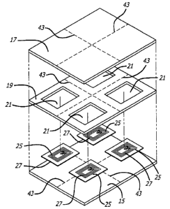
[0018] FIGURE 1 shows imageable electronic-identification sheet assemblies 11
of the present invention both before and after being fed through a laser
printer 13.
Laser printer applied images 33 are printed onto the sheet assemblies 11. Each
of the imageable electronic-identification sheet assemblies 11 is formed from
a
base sheet 15, a cover sheet 17 and a mask sheet 19 (see FIGURES 2 and 4).
The mask sheet 17 has one or more windows 21 formed therein. Four windows
21 are illustrated in the exploded perspective view of an RFID tag or label
sheet
assembly of FIGURE 4.
[0019] The mask sheet 17 is bonded between the base 15 and cover sheets 17
to form one or more protective pockets 23. In the particular embodiment
illustrated in FIGURE 4, the four windows 21 form four protective pockets 23.
Within each protective pocket 23 is one or more electronic circuits 25. Each
electronic circuit 25 can be fit entirely within a protective pocket. The
diagrammatic vertical cross-sectional view of a "protective pocket" region of
an
RFID tag or label of FIGURE 2 in addition to FIGURE 4 illustrates a single
-3-
CA 02484112 2004-10-15
WO 03/090151 PCT/US03/12349
electronic circuit 25 within each of the protective pockets 23. The electronic
circuit
25 can be, for example, an RFID transponder such as one from the Tag-it~ HF-I
Transponder Inlay series from TEXAS INSTRUMENTS.
[0020] The unique protective pockets 23 protect the electronic circuits 25
from
the heat and pressure applied by the laser printer 13 when printing an image
on
the cover sheet 17. The walls forming the windows 21 of the mask 19 absorb
some of the pressure exerted by the feed rollers of the laser printer 13. The
base
sheet 15 and cover sheet 17 also help to spread some of the pressure away from
the electronic circuit 25. The base sheet 15 and cover sheet 17, in addition
to the
protective cavity 23, also serve to insulate and channel away the heat of the
laser
printing from the electronic circuit 25.
[0021] Within the protective pocket 23 is a transmission device 27 for
communicating identification information 29 from the electronic circuit 25 to
an
external transceiver 31 outside the protective pocket 23. The transmission
device
27 can be a helical antenna portion of the electronic circuit 25 as
illustrated in
FIGURES 2 and 4. The electronic circuit 25 includes a microchip 35
electrically
connected to the transmission device 27.
[0022] The base sheet 15, cover sheet 17 and mask sheet 19 can be of any size
that can be fed through a laser printer, however, H'h x 11 inch, A-4 or other
standard-size paper is desirable because of lower cost and greater
compatibility
with standard printers and software packages used to design the laser printer
applied images 33.
[0023] The entire sheet assembly 11 should have a thickness such that it will
fit
through the laser printer 13 for printing the images 33. For use with standard
laser printers, a sheet assembly thickness of less than 15 (fifteen)
thousandths of
an inch (mils) thick is generally appropriate for enabling feeding through a
laser
printer. The sheet assembly can be formed using permanent adhesive 37 to bond
the base sheet 15 to the mask sheet 19 and the electronic circuit 25. In a
particular embodiment, the electronic circuit 25 is formed on a mounting sheet
39
which is bonded to the base sheet 15 using the permanent adhesive 37. The
mounting sheet 39 can be made from polyester. Rubber or other types of
adhesives can be used to bond the sheet assembly together.
-4-
CA 02484112 2004-10-15
WO 03/090151 PCT/US03/12349
[0024) The base sheet 15 and cover sheet 17 can be 20 pound bond paper
while the mask sheet 19 can be 60 pound or 80 pound bond paper, for example.
The windows 21 can be approximately 6 cm x 8.5 cm. These paper thicknesses
and window sizes work well to protect the electronic circuits 25 from the
pressure
and heat of the laser printer. Of course other paper thickness and window
sizes
can be used as well with electronic circuits 25 of different footprints and
with
different laser printers. The base sheet 15 and cover sheet 17 can also have
thicknesses approximately in the range of 3-4 mils while the mask sheet 19 can
have a thickness approximately in the range of 3-8 mils and preferably
approximately 6 mils. The layers of adhesive 37 holding the base sheet 15 and
cover sheet 17 to the mask sheet 19 and holding the electronic circuit 25 to
the
base sheet can be approximately 1 mil thick. The electronic circuit can be 6
mils
or less high in order to fit into the protective pocket 23. However, the
height of the
electronic circuit can vary in different embodiments. For example, if thinner
paper
is used for the base sheet 15 and the cover sheet 17 while thicker paper is
used
for 'the mask sheet 19, then a taller electronic circuit can be used while
maintaining the thickness of the sheet assembly thin enough to pass through
the
laser printer 13. Similarly, using a thinner mounting sheet 39, or not using
the
mounting sheet 39 at all, allows for greater height within the protective
pocket 23
for utilizing a taller electronic circuit. In some embodiments the height of
the
electronic circuit 25, with or without the mounting sheet 39, can be greater
than
the height of the protective pocket 23. In such a case the cover sheet 17 or
base
sheet 15 might bulge out slightly. Alternatively, a portion of the cover sheet
17
can be hollowed out to accommodate the microchip 35.
[0025] In one embodiment the sheet assembly 11 is assembled by applying the
adhesive 37 to the base sheet 15 and then bonding the mask sheet 19 to the to
the base sheet 15. The windows 21 are generally cut out of the mask sheet 19
prior to assembly of the sheet assembly 11. The electronic circuits 25 can
then be
inserted into the windows 21 using a label applicator. Alternatively, the
electronic
circuits 25 can be applied to the base sheet 15 and then the mask sheet 19 can
be bonded to the base sheet 15 with the windows 21 placed around the
electronic
circuits 25. In either case, the cross-sectional footprint of the electronic
circuit 25
can be made to fit within the window 21. The adhesive 37 can then be applied
to
-5-
CA 02484112 2004-10-15
WO 03/090151 PCT/US03/12349
the cover sheet 17 and/or the mask sheet 19 and the cover sheet 17 is bonded
to
the mask sheet 19 so that the electronic circuits 25 are entirely enclosed
within
the protective pockets 23. An adhesive-free region 41 can be formed on the
inner
surface of the cover sheet 17 so that adhesive does not contact the microchip
35.
Thus the electronic circuit 25 is bonded to the base sheet 15 and not to the
cover
sheet 17. In other embodiments the electronic circuit 25 is bonded to both the
cover sheet 17 and base sheet 15 or to the cover sheet 17 alone. The
electronic
circuit 25 can also be placed in the protective pocket 23 without using any
adhesive to secure the electronic circuit 25.
[0026] In embodiments such as that illustrated in FIGURES 1 and 4 utilizing
multiple protective pockets 21 with multiple electronic circuits 25,
provisions are
made for separating the sheet assembly 11 into multiple sub-assemblies 41 each
including a protective-pocket enclosed electronic circuit 25 thereby producing
separate RFID labels or tags. To this end, the sheet assembly 11 can include
separation lines 43. The separation lines 43 can be cleanly die-cut, foi-
example,
or can include cuts and ties. The separation lines43 can be cut into the sheet
assembly 11 following the adhesive bonding steps. In the embodiment of
FIGURES 1, 3 and 4, one vertical and one horizontal separation line 43 is cut
all
the way through the cover sheet 17, mask sheet 19, and base sheet 15 to
separate the sheet assembly into four sub-assemblies each having a protective
pocket 23 enclosed electronic circuit 25.
[0027] The completed sheet assemblies 11 can then be passed through the
printer 13 of FIGURE 1 as described previously to provide customized variable
imprinting on the cover sheet 17. The laser printer 13 can print images on the
sheet assembly 11 such that each of the sub-assemblies 41 has the same or
images different from the other sub-assemblies 41. FIGURE 3 is a top-plan view
of the sheet assembly 11 after passing through the laser printer 13. Each of
the
sub-assemblies 41 has a different image printed on it. In~the given example
the
sub-assemblies 41 are to be used on the dashboard of a vehicle and each has a
different vehicle printed thereon. The particular design to be printed on the
sheet
assemblies 11 can be controlled through a computer associated with the laser
printer 13.
-6-
CA 02484112 2004-10-15
WO 03/090151 PCT/US03/12349
[0028] After printing, the sheet assemblies 11 are separated along the
separation lines 43 to form a plurality of laser imprinted RFID labels or
tags. The
labels, in particular can be manufactured by adding an additional step to the
above described adhesive bonding step. An additional adhesive layer can be
added to the outside of the base sheet 15 along with a liner layer covering
the
additional adhesive layer. Thus, after separating the laser imprinted RFID
labels,
the liner layer can be removed from the back to expose the adhesive layer and
the
label can be stuck to a desired object. Alternatively, the adhesive layer and
liner
layer can be attached to the cover sheet 17.
[0029] The external transceiver 31, diagrammatically illustrated in FIGURE 2,
can include an antenna and a reader as is known in the art. The external
transceiver 31 can also comprise a separate transmitter, receiver and reader.
The
external transceiver 31 sends a command 45 to the electronic circuit 25 and
receives the response 29 from the electronic circuit 25. The electronic
circuit 25
serves as a transponder. The response from the electronic circuit 25 can be
identification information. The identification information is stored in the
microchip
35 and can be an ID code or the microchip 35 can be used as a data carrier,
with
information being written to and updated on the microchip 35 on the fly. It is
advantageous for the microchip 35 to be a passive device so that it does not
require a battery which would increase the size and weight and shorten the
life of
the RFID labels or tags. However, an on-board battery or other power supply
can
be desirable in other embodiments.
[0030] The RFID labels or tags of the present invention can be used in many
applications. For example, the RFID labels or tags can be used as part of a
payment system. The reader of the external transceiver 31 can communicate with
a database of the identification information and corresponding customer
information so that payments can be arranged between customers and the
payment system.
[0031] The RFID labels or tags of the present invention can also be used as
part
of a security system having an indicator for notifying security personnel when
the
external transceiver 31 receives identification information from the RFID
labels or
tags.
_7_
CA 02484112 2004-10-15
WO 03/090151 PCT/US03/12349
[0032] The RFID labels or tags of the present invention can further be used in
systems for such applications as product authentication, ticketing, library
management and supply chain management applications by using the RFID
labels or tags to transmit identification information to the system.
[0033] In yet another application, the RFID labels or tags of the present
invention
can be used as shipping labels or tags corresponding the laser printer applied
image and the identification information provided by the microchip 35 to
goods.
[0034] It is to be understood that the RFID labels or tags of the present
invention
are not limited to operation in the radio frequency range. They can also
operate
using other electromagnetic frequencies. In addition, they can use sound or
different types of radiation to communicate between the protective pocket 23
and
the external transceiver 31. The present invention can also utilize additional
sheets other than just the three described herein. For example, four or more
sheets of paper can be used. Furthermore, the present invention can utilize
materials other than sheets of paper to form the sheet assembly 11. For
example,
plastic sheets can be used instead. The present invention is also not limited
to
use with a laser printer. Other types of printing such as ink-jet, dot-matrix
or web-
printing can be used instead and the protective pocket 23 can still serve to
protect
the electronic circuit 25. Also, the electronic circuit 25 can be placed in
the
protective pocket 23 in orientations other than the orientation described
above.
[0035] It is to be understood that other embodiments may be utilized and
structural and functional changes may be made without departing from the scope
of the present invention. The foregoing descriptions of embodiments of the
invention have been presented for the purposes of illustration and
description. It
is not intended to be exhaustive or to limit the invention to the precise
forms
disclosed. Accordingly, many modifications and variations are possible in
light of
the above teachings. It is therefore intended that the scope of the invention
be
limited not by this detailed description.
_g_