Note: Descriptions are shown in the official language in which they were submitted.
CA 02484700 2004-11-03
WO 03/098667 PCT/US03/13648
1
SUSCEPTOR FOR MOCVD REACTOR
BACKGROUND OF THE INVENTION
Field of the Invention
This invention relates to metalorganic chemical
vapor deposition (MOCVD) reactors and more particularly
to susceptors used in~MOCVD reactors.
Descri tion of the Related Art
Growth of gallium nitride (GaN) based semiconductor
devices in MOCVD reactors is generally described in
DenBaars and Kelley, Semiconductors and Semimetals, Vol.
50, Academic Press Inc., 1997, p. 11-35. MOCVD is a
nonequilibrium growth technique that relies on vapor
transport of the precursers and subsequent reactions of
group III alkyls and group V hydrides in a heated zone.
Growth gasses and dopants are supplied to the reactor and
are deposited as epitaxial layers on a substrate or
wafer. One or more wafers usually rest on a structure of
graphite called a susceptor that can be heated by a radio
frequency (RF) coil, resistance heated, or radiantly
heated by a strip lamp or coil heater. During the growth
process, the heated susceptor heats the wafers.
FIG. 1 shows a conventional susceptor 10 that is
used in MOCVD reactors such as those provided by Thomas
Swan Scientific Equipment Limited. It has a hollowed
CA 02484700 2004-11-03
WO 03/098667 PCT/US03/13648
2
cylindrical shape and is mounted over the reactor's
heating element at the bottom of the reactor, below the
source gas inlet. It has a circular base plate 12 and
cylindrical sleeve 13, with the circular plate 12 having
a series of disk shaped depressions 14 equally spaced
around the susceptor's longitudinal axis. Each of the
depressions 14 can hold a semiconductor wafer during
growth. When the susceptor 10 is heated by the heating
element the semiconductor wafers are also heated. When
source gases enter the MOCVD reactor, they combine and
then deposit on the heated semiconductor wafers as
epitaxial layers. The susceptor 10 can typically spin at
speeds in the range of 1, 000 to 2, 000 rpm, which results
in. more uniform epitaxial layers on the wafers.
Conventional susceptors 10 are usually formed from a
monolithic structure of graphite or coated graphite that
absorbs heat from the heater element and conducts it to
the wafers in contact with the susceptor 10. The entire
susceptor 10 is heated uniformly to achieve consistent
growth conditions across the surfaces of the wafers.
During fabrication of the epitaxial layers, materials
will not only deposit on the heated wafer, but will also
deposit on the heated susceptor 10. This can cause
deposition of significant amounts of GaN, InGaN, AlInGaN,
and similar compounds on the susceptor surfaces. The
result is a buildup of reaction deposits on the susceptor
that can adversely impact subsequent fabrication steps.
For instance, the deposits can act as impurities during
subsequent growth of the epitaxial layers and can also
result in poor interfaces transition between different
layers. For example, if a layer using an indium source
CA 02484700 2004-11-03
WO 03/098667 PCT/US03/13648
3
gas was grown, indium can be deposited on the susceptor
and though the next layer to be grown does not include
indium, indium from the susceptor surfaces can be
included in the transition between layers. These
impurities can cause poor device performance and can
prevent consistent reproduction of semiconductor devices
on the wafer.
Another disadvantage of conventional susceptors is
that the heating element heats the entire susceptor, not
just the areas under or around the wafers. This requires
large amounts of heat because the susceptor has a
relatively large surface area in comparison to the
wafers. Most of the energy is wasted by not heating the
wafers. This taxes the heater, contributing to early
heater failures. Also, more reactants are consumed due to
the fact that the entire susceptor is at a temperature
sufficient for chemical vapor deposition.
Another disadvantage of conventional susceptors is
that they are difficult to manufacture. They must be
machined from a large section of graphite and if any part
of the susceptor is damaged the entire structure can be
unusable. The fabrication of the depressions can be
extremely difficult because they are off set from the
structure's longitudinal axis. The depressions cannot be
machined using a simple lathe, but must involve more
'complex processes. For the same reasons it is very
difficult to modify the shape of the surface of the
depressions to compensate for temperature non-uniformity.
CA 02484700 2004-11-03
WO 03/098667 PCT/US03/13648
4
SUMMARY OF THE INVENTION
The presei~.t invention discloses a susceptor for
holding semiconductor wafers in a reactor during growth
of epitaxial layers on the wafers. The susceptor
comprises a base structure having a base plate and a
sleeve that are both made of a material having low
thermal conductivity at high temperature. The base plate
has one or more plate holes. One or more heat transfer
plugs are also included, with each plug housed within a
respective one of the one or more plate holes. The heat
transfer plugs are made of a material with high thermal
conductivity at high temperatures to transfer heat to the
semiconductor wafers.
The present invention also discloses a reactor for
growing epitaxial layers on semiconductor wafers,
including a reactor chamber housing a heating element and
susceptor. The susceptor holds the semiconductor wafers
and is arranged over the heater element. The susceptor
comprises a base structure having a base plate and a
sleeve and that are made of a material having low thermal
conductivity at high temperature, with the base plate
having one or more plate holes with a heat transfer plug
held within a respective one of the plate holes. The
wafers are arranged on the plugs, and the plugs are made
of a material with high thermal conductivity at high
temperatures. The plugs transfer heat from the heater
element to the semiconductor wafers. A growth gas inlet
is also included to provide gasses to grow epitaxial
layers on the semiconductor wafers.
Reduced amounts of reactants are deposited on the
susceptor embodiments disclosed herein, thereby reducing
CA 02484700 2004-11-03
WO 03/098667 PCT/US03/13648
unwanted impurities during subsequent fabrication steps.
The epitaxial layers can also be grown using less energy
and consuming less source material because most of the
heat from the reactor's heating element passes through
5 the heat transfer plugs instead of heating the entire
susceptor. The susceptor can also be manufactured using
less complex processes because it does not need to be
machined from a solid piece of graphite. Also, the heat
transfer plugs can be more easily machined so that their
surface adjacent to the wafer has a convex or concave
shape to compensate for any temperature not-uniformity.
These and other features arid advantages of the
invention will be apparent to those skilled in the art
from the following detailed description, taken together
with the accompanying drawings, in which:
BRIEF DESCRIPTION OF THE DRAWINGS
FIG. 1 is a perspective view of a ~ prior art
susceptor;
FIG. 2 is a 'perspective view of a susceptor
according to the present invention;
FTG. 3 is a sectional view of the susceptor in FIG.
2, taken along section lines 3-3;
FIG. 4 is an exploded view of the susceptor in FIG.'
2t
FIG. 5 is a plan view of a heat transfer plug used
in the susceptor of FIG. 2;
FIG. 6a is a sectional view of the plug in FIG. 5,
taken along section lines 6a-6a;
FIG. 6b is a sectional magnified view of a plug
ridge shown in FIG. 6a; and
CA 02484700 2004-11-03
WO 03/098667 PCT/US03/13648
6
FIG. 7 is a simplified diagram of an MOCVD reactor
using a susceptor according to the present invention.
DETAILED DESCRIPTION OF THE INVENTION
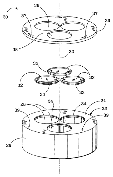
FIGS. 2 through 4 show a susceptor 20 according to
the present invention, which can hold substrates or
wafers for growth of epitaxial layers in an MOCVD
reactor. The susceptor 20 can be mounted over the MOCVD
reactor's heating element at the bottom of the reactor
and can spin during the growth process.
The susceptor 20 includes a base structure 22 made
of a base plate 24 and a cylindrical sleeve 26, which can
be separate or manufactured as one structure. The base
plate 24 has circular through holes 28 equally spaced
around the susceptor's longitudinal axis 30. The number
of through holes 28 can vary depending on the number of
wafers that the susceptor 20 is designed to hold during
growth.
The base structure 22 should be made of a rigid
material that has a low thermal conductivity at high
temperature so that it transmits less heat from the MOCVD
reactor's heating element. It should also be made of a
material that is reflective so that it reflects the
heating element's radiative heat to further reduce the
amount of heat it transmits. It should also have a low
thermal expansion, so that its expansion matches that of
the other susceptor components.
The base structure 22 can be made of many different
materials such as boron nitride, fused quartz, aluminum
, nitride, or a ceramic,, with the aluminum nitride and
ceramic embodiments being coated with a material to
CA 02484700 2004-11-03
WO 03/098667 PCT/US03/13648
7
reduce their reactance with the source gasses. A
preferred base structure 22 is made of boron nitride or
fused quartz covered by boron nitride. These materials
have high thermal conductivity at low temperature, low
thermal conductivity at high temperature, and boron
nitride is, white, which enhances the structure's
reflectivity. The base structure 22 is manufactured using
known methods.
The base structure 22 can have many different
dimensions. A suitable height for the cylindrical sleeve
is approximately 2 inches and a suitable diameter is
approximately 6.2 inches for a susceptor holding three 2
inch wafers. The base plate 24 also has a suitable
diameter of approximately 6.2 inches, with the plate
holes 28 equally spaced around the center of the base
plate 24. A suitable diameter for the plate holes 28 is
approximately 2.3 inches. The base plate 24 and the
sleeve 26 can have many different thicknesses, with a
suitable thickness being approximately 0.2 inches.
The susceptor 20 also includes heat transfer plugs
32, each of which fit within a respective plate hole 28.
Semiconductor wafers are placed in contact with the plugs
32 during growth of the epitaxial layers and heat from
the heating element should be efficiently conducted
through the plugs 32, to the wafers. The plugs 32 a-re
preferably made of a material having high thermal
conductivity at high temperature and a dark color, both
of which promote heat conduction. The preferred material
for the plugs 32 is graphite or silicon carbide coated
graphite. Each of the plugs 32 has an axial lip 33 around
its outer surface, which rests on one of the axial ledges
CA 02484700 2004-11-03
WO 03/098667 PCT/US03/13648
8
34 on the inside surfaces of the through holes 28, such
that a respective plug 32 rests within one of the holes
28. '
A faceplate 36 can also be included that has holes
38 that align with the base structure's plate holes 28.
The faceplate is arranged on the base structure's base
plate 24 with the faceplate and base structure holes 38,
28 aligned. Only the plugs 32 are uncovered by the
faceplate holes 38 and when a wafer is placed over the
plug 32, only the wafer is uncovered by the holes 38.
The susceptor 20 works without the faceplate 36, but
small amounts of reactants can deposit on the base
structure 22 during epitaxial growth. The faceplate 36
provides a surface with a greater resistance to
deposition of reaction species, with the surface also
being easy to clean. It is preferably infrared
transparent so that is does not absorb optical heat. It
should also be made of a material that does not react
with MOCVD source gasses. It can be made of materials
such as quartz, pure silicon carbide, sapphire, silicon,
coated graphite, graphite or tungsten, with a preferred
material being quartz. Deposits can be cleaned from
quartz by etching.
The faceplate 36 should have approximately the same
diameter as the base plate 22 and its holes 38 should
have the same or slightly smaller diameter as the plate
holes 28. The faceplate 36 can have many different
thicknesses with a suitable thickness being approximately
0.16 inches.
The susceptor 20 is designed to spin over the
reactor's heating element during growth, so the face
CA 02484700 2004-11-03
WO 03/098667 PCT/US03/13648
9
plate 36 should be mounted to the base structure 22.
Different mounting methods can be used including, but not
limited to, pins on the structure 22.mated with mounting
holes, axial. slots or J-slots in the faceplate 36.
Alternatively, rotatable hooks can be included on the
structure to mate with slots in the faceplate 36. In one
embodiment, the hooks can be turned away from the center
of the base plate 24 and the faceplate 36 is then placed
over the base plate 24, with the stem of the hooks
aligned with a respective slot. The hooks are then
rotated so they are directed toward the center of the
base plate 24. In the embodiment shown in FIGS. 2 through
4, ,the faceplate has axial slots 37 that mate with pins
39 on the structure 22. Each pin 39 has a head that
passes through the widest section of one of the slots 37.
The faceplate is then turned until the stem of each pin
39 is housed within the narrow section of its respective
slot 37.
A space can be included between the faceplate 36 and
the base structure 32 to limit the conducted heat due to
contact between the faceplate 36 and the base plate 24.
This is best accomplished by including a raised section
on the surface of the base plate 24, around its edge.
The susceptor 20 can be used in MOCVD reactors where
the susceptor is arranged at the bottom of the reactor
with the circular plate facing up. Growth gasses enter
the reactor from the top or sides and are deposited on
the uncovered wafers that are held over the plugs 40.
This susceptor 20 promotes the transfer of heat from
the reactor's heating element through the plugs 32, which
reduces the amount of deposits on the surface of the base
CA 02484700 2004-11-03
WO 03/098667 PCT/US03/13648
structure 22. Reduction of such deposits reduces the
presence of unwanted compounds during fabrication of
subsequent layers. The fabrication process requires less
growth gas because most of the gasses are deposited on
5 the wafer. The resulting semiconductor device has sharper
interfaces and lower levels of unwanted impurities. This
increases the yield and reproducibility of the epitaxial
growth process.
This design also reduces the amount of power
10 required to maintain the wafers at any given temperature
compared to conventional susceptors. The heat primarily
passes through the plugs only, instead of the entire
susceptor as in the prior art. This allows for the use of
smaller and less expensive components in the heater
control assembly, increases the life of the heater
assembly, and allows the growth of the epitaxial layers
using less energy and source gasses.
FIGS. 5 and 6 show one embodiment of a heat transfer
plug 50, according to the present invention. Each plug 50
is substantially puck shaped and is designed to transfer
heat from the reactor's heating element to a
semiconductor wafer 52 (shown in FIGS. 6a and 6b) held
in contact with the plug 50. The plug 50 can have a
circular ridge 54 on its surface adjacent to the wafer
52, with only the ridge 54 contacting the wafer. This
provides a small space between the wafer 52 and the plug
50 to promote even convective heating of the wafer. To
further promote even heating of the wafer 52, the surface
of the plug 50 adj acent to the wafer 52 can also have a
convex, concave, or other shaped surface. The plug 50
should have a diameter that allows it to fit one within
CA 02484700 2004-11-03
WO 03/098667 PCT/US03/13648
11
one of the base plate through holes 28 and should have a
size which allows lfor thermal expansion of the plug or
base plate, with a suitable diameter being approximately
2.l inches. Each plug 50 has a lip 56 (shown as reference
number 33 in FIGS. 3 and 4) around its edge so that the
plug's top section of has a slightly larger diameter than
its lower section. As described above, each plug's lip 56
rests on a respective hole ledge 34.
The plug can have many different thicknesses, with
l0 a suitable thickness being approximately 0.33 inches. The
ridge 54 can be many different sizes, with a suitable
size being 0.002 inches high and 0.003 inches wide.
Prior to growth of the epitaxial layers, the wafers
52 and transfer plugs 50 are ,placed in the through holes
28 and the faceplate 36 is mounted to base structure 22
with the faceplate holes 38 aligned with the base
structure's holes 28. The wafers 52 are uncovered by the
faceplate 36 and when the plugs 50 are heated by the
MOCVD's heating element, the wafers 52 are also heated.
Growth gasses are fed into the reactor as the susceptor
assembly 20 spins and epitaxial layers are grown on the
wafers 52.
FIG. 7 shows one embodiment of an MOCVD reactor 70
that can utilize a susceptor in accordance with the
present invention for growing epitaxial layers on a
wafer. The reactor 70 comprises a reaction chamber 72
having growth susceptor 74 that can spin. One or more
wafers are mounted on the susceptor 74 for growth of
epitaxial layers. During growth, the susceptor 74 is
heated by a heater element (not shown) that is arranged
within the susceptor 74, adjacent to the wafers. The
CA 02484700 2004-11-03
WO 03/098667 PCT/US03/13648
12
heating element can be a variety of heating devices but
is usually a radio frequency (RF) coil, resistance coil,
or a strip heater.
A carrier gas 76 is supplied to a gas line 78, the
carrier gas being an inert gas such as hydrogen or
nitrogen. The carrier gas 76 is also supplied through
mass flow controllers 80a, 80b, 80c to respective
bubblers 82a, 82b, 82c. Bubbler 82a can have a growth
compound, such as an alkylated compound having a methyl
group, e.g. trimethyl gallium (TMG), trimethyl aluminum
(TMA) or timethyl indium (TMI) . Bubbler 82b and 82c may
also contain a similar methyl group compound to be able
to grow an alloy of a Group III compound. The bubblers
82a, 82b, 82c are typically maintained at a predetermined
temperature by constant temperature baths 84a, 84b, 84c
to ensure a constant vapor pressure of the metal organic
compound before it is carried to the reaction chamber 72
by the carrier gas 76.
The carrier gas 76, which passes through bubblers
82a, 82b, 82c, is mixed with the carrier gas 76 flowing
within the gas line 78 by opening the desired combination
of valves 86a, 86b, 86c. The mixed gas is then
introduced into the reaction chamber 72 through a gas
inlet port 88 formed at the upper end of the reaction
chamber 72. A shower head inlet (not shown) can be
included at the inlet port 88.
A nitrogen containing gas 90 such as ammonia, is
supplied to the gas line 78 through a mass flow
controller 92 and the flow of nitrogen containing gas is
controlled by valve 94. If the carrier gas 76 is mixed
with the nitrogen containing gas 90 and the TMG vapor
CA 02484700 2004-11-03
WO 03/098667 PCT/US03/13648
13
within the gas line 78 and then introduced into the
reaction chamber 72, the elements are present to grow
gallium nitride on the wafer through thermal
decomposition of the molecules present in the TMG and
ammonia containing gas.
To dope alloys of gallium nitride on the wafer, one
of the bubblers 82a, 82b, 82c not being used for the TMG
is used for a dopant material, which is usually Magnesium
(Mg) or Silicon (Si), but can be other material such as
beryllium, calcium, zinc, or carbon. Bubbler 82b or 82c
can be used for an alloy material such as boron aluminum,
indium, phosphorous, arsenic or other materials. Once
the dopant and alloy are selected and one of the valves
86a, 86b, 86c is opened to allow the dopant to flow into
gas line 78 with the gallium and nitrogen containing gas
90, the growth of the doped layer of gallium nitride
takes place on wafer.
The gas iaithin the reaction chamber 72 can be purged
through a gas purge line 96 connected to a pump 98
operable under hydraulic pressure. Further, a purge
valve 100 allows gas pressure to build up or be bleed off
from the reaction chamber 72.
The growth process is typically stopped by shutting
off the gallium and dopant sources by closing valves 86a
and 86b, and keeping the nitrogen containing gas and the
carrier gas flowing. Alternatively, the reaction chamber
72 can be purged with a gas 102 that can be controlled
through a mass flow controller 104 and valve 106. The
purge is aided by opening valve 100 to allow the pump 98
to evacuate the reaction chamber 72 of excess growth
gasses. Typically, the purge gas 102 is hydrogen, but can
CA 02484700 2004-11-03
WO 03/098667 PCT/US03/13648
14
be other gasses. The wafer is then cooled by turning off
power to the heater element.
Although the present invention has been described in
considerable detail with reference to certain preferred
configurations thereof, other versions are possible. The
susceptors according to the present invention would work
without a faceplate 36. As described above, susceptors
according to the present invention can be used in many
different reactors beyond MOCVD reactors and can be used
in many different types of MOCVD reactors. The susceptors
can be made of many different materials with many
different dimensions. They can also be arranged
differently with one different arrangement having the
plugs 32 housed within the faceplate holes 38. Therefore,
the spirit and scope of the appended claims should not be
limited to the preferred versions. in the specification.