Note: Descriptions are shown in the official language in which they were submitted.
CA 02486240 2008-08-06
SWITCHED RESONANT ULTRASONIC POWER AMPLIFIER SYSTEM
BACKGROUND OF THE INVENTION
1. Technical Field
The present disclosure relates to devices for amplifying an input signal
and providing an output signal to a surgical instrument. More particularly,
the present
disclosure relates to a switched resonant ultrasonic power amplifier system
for surgical
instruments.
2. Background of Related Art
Conventional power amplifier circuits for supplying drive signals to
ultrasonic transducers are susceptible to drift and droop in power delivery
and variations
in frequency when the ultrasonic transducer is exposed to changing loading
conditions.
Additi0hally, conventional power amplifier circuits require a relatively large
footprint, are
1
CA 02486240 2011-01-07
not lightweight, have efficiency problems, are generally complex circuits, and
require heat sinking to dissipate heat generated during operation. Due to
their
relatively large size and radiated heat, placement of conventional power
amplifier circuits may be problematic in a medical treatment facility.
Therefore,
a need exists for a power amplifier circuit to supply a drive signal to an
ultrasonic transducer and which overcomes the problems of conventional
power amplifiers.
SUMMARY
A switched resonant ultrasonic power amplifier system that has
improved operating efficiency is provided. The switched resonant ultrasonic
power amplifier system of the present disclosure has reduced heat generating
characteristics and a smaller footprint than conventional power amplifiers.
Furthermore, the switched resonant ultrasonic power amplifier system includes
compensation circuitry for changing tissue loads during system operation,
structure for frequency, phase and gain stabilization and structure for
ultrasonic
power loss compensation.
In accordance with one embodiment of the present invention,
there is provided a system for controlling an output of an ultrasonic device.
The
system includes a switched resonant power amplifier receiving and processing
a driver output signal for generating a drive signal that is provided to an
ultrasonic device for controlling the output of the ultrasonic device. An
output
control circuit is provided comprising a wave shaping circuit having a zero
crossing detector receiving and processing a feedback signal related to the
2
CA 02486240 2011-01-07
output of the ultrasonic device and generated by the ultrasonic device. The
zero crossing detector generates a corresponding square wave signal. The
wave shaping circuit further includes a comparator comparing the square wave
signal to a reference signal for generating a reset signal having a
substantially
identical frequency to the feedback signal. The output control circuit further
includes a compensating circuit having a reference timer for receiving and
processing the reset signal for generating a compensated reference signal
having substantially the same frequency as the reset signal and substantially
180 out-of-phase with respect to the reset signal, wherein frequency and
amplitude characteristics of the compensated reference signal are determined
by at least the reset signal. The compensating circuit further includes a
phase
locked loop (PLL) receiving first and second input signals, wherein the first
input signal is the compensated reference signal and the second input signal
is
a divider reference signal, and wherein the PLL processes the first and second
input signals for generating a compensated clock signal that is adjusted for
at
least one of phase and frequency differences between the received first and
second input signals. A compensated drive circuit is operatively coupled to
the
compensating circuit, the compensated drive circuit comprising divider
circuitry
for stepping down the frequency of the compensated clock signal to a
selectable frequency for generating a counter output signal; flip-flop
circuitry for
splitting the counter output signal into first and second complementary square
waves together forming a driver input signal, wherein a sample of at least one
of the first and second complementary square waves is the divider
reference signal; and a driver for amplifying the driver input signal for
2a
CA 02486240 2011-01-07
generating the driver output signal.
The present disclosure relates to a switched resonant ultrasonic
power amplifier system including a switched resonant power amplifier. The
power amplifier system further includes a wave shaping circuit, a frequency
generating and compensating circuit, and a compensated drive circuit. The
switched resonant power amplifier generates a transducer driver signal for
driving an ultrasonic transducer. The wave shaping circuit includes a zero
crossing detector and a comparator. A feedback signal from the ultrasonic
transducer is generally sinusoidal and is applied to an input of
15
2b
CA 02486240 2004-10-28
the zero crossing detector where it is transformed into a square wave. The
square
wave output of the zero crossing detector is capacitively coupled to the input
of the
comparator to form a reset signal.
The frequency generating and compensating circuit includes a reference
timer and a phase-locked loop. The reset signal is applied to an input of the
reference
timer to generate a compensated reference signal having a substantially
identical
frequency that is further applied to an input of the phase-locked loop. The
phase-locked
loop outputs a compensated clock signal at a particular frequency that is
controllable by
the compensated reference signal applied to the input of the phase-locked
loop. The
compensated clock signal is generally at a different frequency than the
desired output
signal to be applied to the ultrasonic transducer.
The phase locked loop compares the compensated reference signal to a
divider reference signal for generating a frequency error signal and/or a
phase error
signal; The phase locked loop provides frequency compensation by adjusting the
compensated clock signal according to a value of the frequency error signal.
In
addition, it may include a phase delay circuit for adjusting the phase
relationship
between the compensated reference signal and the divider reference signal
according
to a value of the phase error signal. Generally, the phase locked loop
receives digital
input signals from the drive circuit and the wave shaping circuit.
Alternatively, the phase
locked' loop may be configured and adapted for mixed-mode signal processing
where
the inputs are a combination of analog and digital signals. By advantageously
adjusting
3
CA 02486240 2004-10-28
the compensated clock signal for frequency and/or phase, the ultrasonic power
ampler
system compensates the gain of the ultrasonic amplifier system.
The compensated clock signal is applied to an input of the compensated
drive circuit. The compensated drive circuit includes a divider, a flip-flop,
and a driver.
A selected step-down ratio is applied to the compensated clock signal in the
divider that
results in a counter output signal delivered by the divider to the flip-flop,
which has a
lower frequency than the compensated clock signal. The counter output signal
has a
frequency that is approximately double the selected operating frequency for
the
ultrasonic transducer. A further reduction in frequency occurs as the counter
output
signal is applied to the flip-flop. The flip-flop generates two complementary
square
waves that are substantially 180 out-of-phase with respect to each other.
Each of the
square waves has a frequency that is at the selected operating frequency for
the power
amplifier and approximately one-half of the frequency of the counter output
signal.
These complementary square waves are applied to inputs of the driver for
amplification
and transmission to the inputs of the switched resonant power amplifier as
driver output
signals.
In another preferred embodiment, the driver includes a phase delay circuit
that cooperates with the driver and provides phase compensation for the
switched
resonant power amplifier input signals. By controlling the phase relationship
between
the input signals, the driver is now phase correlated and random phase
relationships
are significantly minimized.
4
CA 02486240 2004-10-28
The switched resonant power amplifier includes. a pair of insulated gate bi-
polar transistors that receive the driver output signals. The insulated gate
bi-polar
transistors are biased such that when one is conducting the other one is not
conducting,
since one driver output signal has a value that corresponds to a "high" value,
while the
complementary driver output signal has 2 value that corresponds to a "low"
value.
When the driver signals change states (e.g,, high to low and low to high), the
respective
insulated gate bi-polar transistors change from a conducting. state to a non-
conducting
state, thereby providing an output to a primary side of an output transformer.
On a
secondary side of the output transformer is a pair of DC blocking output
capacitors
further coupled to an input of an ultrasonic device. The waveforms on the
primary side
of the output transformer are coupled across to a secondary side of the output
transformer, where the waveforms combine to form the transducer driver signal.
The
ultrasonic device includes an ultrasonic transducer and a feedback transducer
that are
operatively coupled to the secondary side of the output transformer. The
ultrasonic
transducer receives the transducer drive signal from the output transformer
and drives
the transducer element to deliver the ultrasonic energy. The feedback
transducer
generates the feedback signal that is coupled to the wave shaping circuit.
In addition, the ultrasonic power amplifier system includes an output
control circuit. The output control circuit includes the frequency generating
and
compensating circuit and the drive circuit. It cooperates with the wave
shaping circuit
for real time monitoring and control. The reset signal, that is representative
of the
5
rr - z s.. .,. uY are .,-;, .., :'i...'.. fa1'G .a'"..#.x.a1a',., .b Yfi,
<.'~`: u 'OF9+5 ,v='-w"r.tl.$'u a-,Rf n-'Mi~ YV.'t ~"a' rcoFF+ r'=s`m,.a` /
scc lrcF4 -..rr-m ml,, -.-r a-.''.." .:,.-.rw....,m .,.xr w> ,zxw+.m.
rmmrranrn^e; aa-zrre ,'~ls*S *'_
CA 02486240 2004-10-28
feedback signal, is received by the frequency generating and compensating
circuit for
generating a compensated clock circuit. The divider reference signal is
compared to the
compensated reference signal in real time to control the compensated clock
signal for
frequency, phase, and/or gain, Additionally, the drive circuit includes a
phase delay
drive disposed in the driver for additional phase compensation between
switched
resonant power amplifier input signals. By providing real time monitoring and
control of
the drive signal to the ultrasonic device, the ultrasonic power amplifier
system is
capable of automatically monitoring and controlling the output of the
ultrasonic device.
BRIEF DESCRIPTION OF THE DRAWINGS
Embodiments of the presently disclosed switched resonant ultrasonic
power amplifier system are described herein with reference to the drawings,
wherein:
FIG. 1 is block diagram of a switched resonant, ultrasonic power amplifier
system in accordance with an embodiment of the present disclosure; and
FIG. 2 is a schematic diagram of an embodiment of a switched resonant
power amplifier of FIG. 1 in accordance with the present disclosure.
4
6
CA 02486240 2004-10-28
DETAILED DESCRIPTION
Embodiments of the presently disclosed switched resonant ultrasonic
power amplifier system will now be described in detail with reference to the
drawings, in
which like reference numerals and characters designate identical or
corresponding
elements in each of the drawings.
As mentioned above, conventional power amplifier circuits, which supply
drive signals to ultrasonic transducers, are typically susceptible to so-
called "drift" and
"droop" in power delivery and variations in frequency when the ultrasonic
transducer is
exposed to changing loading conditions. Moreover, conventional power amplifier
circuits are typically very complex (e.g., complex circuitry),. require a
relatively large
footprint and are quite burdensome, suffer from efficiency problems, and
require a heat
sink (or other cooling means) to dissipate heat generated during operation. As
a result,
placement of conventional power amplifier circuits may be problematic in a
medical
treatment facility.
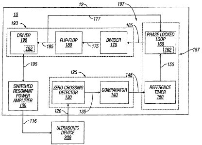
Referring to FIG. 1, an exemplary embodiment of the presently disclosed
switched resonant ultrasonic power amplifier system 10 is illustrated.
Switched
resonant ultrasonic power amplifier system 10 is enclosed by box 12 in FIG. 1
and
includes a switched resonant power amplifier 100, a wave shaping circuit 125
having a
zero crossing detector 130 and a comparator 140, and a frequency generating
and .~
compensating circuit 157 having a reference timer 150 and a Phase locked loop
("PLL")
7
CA 02486240 2004-10-28
160. The switched resonant ultrasonic power amplifier system 10 further
includes a
compensated drive circuit 193 having a divider 170, a flip-flop 180, and a
driver 190. An
ultrasonic device 200 includes an ultrasonic transducer 114 and a feedback
transducer
118 (as shown in FIG. 2) for receiving a transducer driver signal 116 that is
an output of
the switched resonant power ampler 100. Preferably, driver signal 116 is
applied to
ultrasonic transducer 114. A feedback signal 120 is generated by the feedback
transducer 118 and is communicated to zero crossing detector 130. Feedback
signal
120 is proportional to driver signal 116 with substantially similar phase and
frequency
values and generally lower voltage values.
As shown in FIG. 2, switched resonant power, amplifier 100 includes a
plurality of switching elements 102A, 1028; a corresponding number of resonant
tuning
components or elements including a tuning capacitor 104A, 104B and a tuning
inductor
106A, 1068; and an output transformer 108. Tuning capacitors 104A, 1048 and
tuning
inductors 106A, 106B form first and second tuning circuits 109A, 109B
respectively.
Output transformer 108 is operatively coupled to an input of ultrasonic
transducer 114.
A variety of devices may be used for switching elements 102A, 102B, including'
relays,
metal oxide semiconductor field effect transistors ("MOSFET"), and insulated
gate
bipolar transistors ("IGBT").
In operation, driver 190 provides at least one driver output signal 195 that
is coupled to the input of at least one switching element 102. Driver output
signal 195
includes a corresponding number of input signals 195A, 1958 to the number of
8
CA 02486240 2004-10-28
switching elements 102A, 102E of switched resonant power amplifier 100. Each
switching element 102A, 102B is capable of producing an amplified output of
the
respective input signals 195A, 1958. A supply voltage VDC is supplied through
tuning
inductors 106A, 106B to switching elements 102A, 102B where tuning inductors
106A,
106B are connected in a series relationship to a supply lead of each switching
element
102A, 102B. Tuning capacitors 104A, 1048 are connected in a parallel
relationship to
an output lead of each switching element 102A, 102B.
The amplified output of each switching element 102A, 10231s coupled to
the corresponding tuning circuit 109A, 109B. Tuning capacitors 104A, 104B and
tuning
inductors 106A, 106B are selected to correspond to a particular resonant
frequency of
input signals 195A, 195B. For example, if the selected transducer driver
signal 116 has
a frequency of 23 KHz, i.e., a period of 43.5ps, then the tuned period for
each switching
element 102A, 102B is 21.75 Ns. The tuned period for tuning circuits 109A,
1098 is
defined by the formula T = IT (LC)1'2 , where L is the value of tuning
inductors 106A,
106B, C is the value of tuning capacitors 104A, 1048, and T is the tuned
period.
Output transformer 108, in cooperation with output capacitors 110 couples
the amplified output of switching elements 102A, 102B, or driver signal 116,
to
ultrasonic transducer 114. Output capacitors 110 are connected in a series
arrangement with the secondary coil of output transformer 108. Using output
capacitors
110 in a series arrangement substantially blocks any residual direct current
("DC") and
passes substantially all the alternating current ("AC') on the secondary side
of output
9
____.V ..:5`.1SPC.3:Tx,..t8"J`r'.YV. Rr e'u?CMA,,.e41.iTr9.y.e"2iMt`
2tlFxn*x`:.in."bY+1Lrv ..4RXCeE. rsmXttl ..n.msrt.xrmarrcz.m.'mear wm: ..um
...,m...... ,.,..,......,-m. -ea .c'+:.:mRwsacTS) o..w,..
CA 02486240 2004-10-28
transformer 108. Preferably, output transformer 108 has a ratio of
approximately 1:1
while output capacitors 110 have a value of approximately 101f.
In a preferred embodiment, a pair of IGBTs, used as switching elements
102A, 1028, is disposed in switched resonant power amplifier 100. Driver 190
provides
the pair of input signals 195A, 195B that are coupled to the gates of
switching elements
102A, 1028. Input signals 195A, 195B are square waves that are approximately
180
out of phase with respect to each other. Supply voltage VDC is applied to the
drains, or
collectors, of switching elements 102A, 102B through series connected tuning
inductors
106A, 106B. Tuning capacitors 104A, 104B are additionally connected in
parallel to the
drains, or collectors, thereby defining first and second. tuning circuits
109A, 109B.
Switching elements 102A, 102B further include sources, or emitters, that are
connected
to a chassis common. As each input signal 195A, 195B changes in value, a
corresponding inverse change in the output of switching elements 102A, 1028
occurs.
Each switching element 102A, 102B only conducts when each
corresponding input signal 195A, 195B rises above a threshold value. Using a
pair of
switching elements 102A, 102B permits a first switching element 102A to
conduct (e.g.,
a first input signal 195A is above the threshold value) while a second
switching element
102B does not conduct (e.g., a second input signal 1958 is at or below the
threshold
value), since the corresponding first and second input signals 195A, 195B are
approximately 180 out of phase with respect to each other. After a period of
time,
corresponding to the period of first input signal 195A, has elapsed, first
input signal
CA 02486240 2004-10-28
195A is now at or below the threshold value while second input signal 195B is
above
the threshold value. At this point, first switching element 102A stops
conducting while
second switching element 102B begins conducting, thereby providing a switching
capability of switched resonant power amplifier 100.
Further still, each tuning circuit 109A, 109B is operatively coupled to the
primary side of output transformer 108 and connected in a series relationship
to the
other tuning circuit 109B, 109A respectively. Selecting the values of L and C,
for tuning
inductors 106A, 106B and tuning capacitors 104A, 104B, respectively,
determines the
resonant frequency of first and second tuning circuits 109A, 109B,
respectively.
In an exemplary embodiment, the resonant frequency of each tuning
circuit 109A, 109B is tuned near to the operating frequency of each input
signal 195A,
195B. When first switching element 102A is conducting, it generates a first
output that
is operatively coupled through first tuning circuit 109A. The output of first
switching
element 102A and its associated first tuning circuit 109A is operatively
coupled to the
primary side of output transformer 108 and is preferably an AC half sine wave.
Operation of second switching element 102B and tuning circuit 109B is
substantially similar to the operation of first switching element 102A and
first tuning
circuit 109A as described above- Second switching element 102B does not
conduct
when first switching element 102A conducts, since input signal 195B is
approximately
180 out of phase with respect to input signal 195A. Therefore, the output of
switching
11
CA 02486240 2004-10-28
element 102B is essentially an AC half sine waveform that is complementary to
the
output of switching element 102A and provides a substantially smooth combined
sinusoidal output wave at the secondary side of output transformer 108. The
output
wave has a frequency that is substantially equal to the input frequency of
input signals
195A, 195B.
Output transformer 108 is preferably configured for a 1:1 primary to
secondary ratio where the output waveform is substantially equivalent in
magnitude to
the input waveform. Output capacitors 110 are connected to the secondary side
of
output transformer 108 and generally block any DC component of the output
waveform
that may be present on the secondary side of output transformer 108. In
addition,
output capacitors 110 conduct substantially the entire AC component of the
output
waveform, thereby contributing to the smooth sinusoidal AC output waveform.
The
downstream side of output capacitors 110 is connected to the ultrasonic
transducer 114,
which could be magnetostrictive, piezoelectric, or transducer structures as is
known in
the art.
Ultrasonic device 200 includes feedback transducer 118 for providing
feedback signal 120 to wave shaping circuit 125. Output transformer 108 is
electrically
coupled to ultrasonic device 200 such that electrical power is delivered to
ultrasonic
transducer 114 as transducer driver signal 116 and converted to ultrasonic
power.
Furthermore, switched resonant power amplifier 100 generates transducer driver
signal
116 with the desired signal characteristics (e.g., wave shape, amplitude,
and/or
12
CA 02486240 2004-10-28
frequency) and communicates it to an input of ultrasonic device 200. In a
preferred
embodiment, transducer driver signal 116 is a substantially smooth sinusoidal
AC
waveform with the desired signal characteristics for driving ultrasonic
transducer 114.
Feedback transducer 118 is also disposed on the secondary side of output
transformer 108 and generates feedback signal 120 that is electrically coupled
to zero
crossing detector 130. In a preferred embodiment, feedback signal 120 is a
sample of
transducer driver signal 116 having a waveform with substantially the same
frequency
and wave shape. Since feedback signal 120 and transducer driver signal 116 are
coupled within the ultrasonic device 200, characteristics of feedback signal
120 are
related to characteristics of transducer driver signal 116 and reflect changes
in the
characteristics of the transducer(s) (e.g., ultrasonic transducer 114 and/or
feedback
transducer 118) of the ultrasonic device 200. For example, if the frequency of
transducer driver signal 116 increases with a corresponding decrease in its
period,
feedback signal 120 has a corresponding increase it its frequency and
substantially
matches the frequency change of transducer driver signal 116. Changes in other
characteristics of transducer driver signal 116 result in corresponding
changes to the
respective characteristics of feedback signal 120.
Zero crossing detector 130, in cooperation with associated circuitry,
modifies feedback signal 120 and provides an output that is substantially a
square wave
135. Ina preferred embodiment, zero crossing detector 130 includes a
comparison
circuit, such as an LM393 integrated circuit, having biasing circuitry and a
diode coupled
13
CA 02486240 2004-10-28
to the output of the comparison circuit. Preferably, feedback signal 120 is
coupled to
the input of the comparison circuit for providing a more stable output square
wave 135.
As a component of wave shaping circuit 125, zero crossing detector 130
receives an
analog input signal (e.g., feedback signal 120) and produces a digital output
signal (e.g.,
square wave 135).
By applying feedback signal 120 to an appropriate input lead of the
comparison circuit, zero crossing detector 130 generates square wave 135
having a
waveform representative of feedback signal 120. As feedback signal 120
transitions
above a predetermined (zero) voltage reference point, thereby becoming more
positive,
the comparison circuit conducts and provides a positive -portion of square
wave 135.
The output will be of substantially constant amplitude as long as feedback
signal 120 is
more positive than the zero reference point. When feedback signal 120 is at
the zero
reference point, there is no difference in voltage on the input leads of the
comparison
circuit, thereby causing the comparison circuit to stop conducting, and
provide a zero
output. As a result, the output of the comparison circuit rapidly changes from
a constant
positive value to zero, thereby providing a substantially instantaneous
transition of the
output signal.
Once feedback signal 120 transitions below the zero reference point,
thereby becoming more negative, the comparison circuit again conducts and
provides a
negative portion of square wave 135. Zero crossing detector 130 is biased and
configured to provide a rapid change from the constant positive amplitude to
the
14
CA 02486240 2004-10-28
constant negative amplitude forming the leading and trailing edges of square
wave 135,
such that the edges are substantially vertical. Feedback signal 120 and square
wave
135 have substantially identical frequencies, even if their respective
amplitudes are
different.
Square wave 135 is coupled to comparator 140, where square wave 135
is preferably capacitively coupled to comparator 140. Comparator 140 includes
a
comparison circuit and is preferably coupled to a capacitor coupling circuit
that generally
blocks any DC component of square wave 135 from being transmitted from zero
crossing detector 130 and transmits substantially the entire AC component of
square
wave 135 to comparator 140. In a preferred embodiment, comparator 140 includes
an
IC comparator, such as an LM393 along with associated biasing and feedback
circuitry.
As the amplitude of square wave 135 goes positive past the zero voltage
reference point, it biases comparator 140 such that the output of comparison
circuit
goes negative, thereby causing the output of comparator 140, a reset signal
145, to
become more negative. A portion of reset signal 145 is coupled through the
feedback
circuitry to another input of the comparison circuit, thereby providing
feedback to the
comparison circuit to produce a more stable output (e.g., reset signal 145).
Preferably,
reset signal 145 has a substantially identical frequency to square wave 135
with a
waveform that is substantially 180 out-of-phase with respect to square wave
135.
4
CA 02486240 2004-10-28
Reset signal 145 is communicated to an input of reference timer 150 for
controlling a timing function of reference timer 150. As reset signal 145
drops below a
predetermined reset threshold value, it causes reference timer 150 to reset.
When
reference timer 150 resets, it generates a compensated reference signal 155
having a
substantially identical frequency to reset signal 145, square wave 135, and
feedback
signal 120. Compensated reference signal 155 does not have the same phase
characteristics as reset signal 145, but is essentially 180 out-of-phase with
respect to
reset signal 145 and feedback signal 120. Consequently, compensated reference
signal 155 is substantially in phase with square wave 135.
In an exemplary embodiment, reference timer 150 includes an IC timer,
such as a 555 precision timer, having associated biasing and feedback
circuitry.
Reference timer 150 in cooperation with the biasing circuitry is configured
for operation
as an astable multivibrator that produces a square wave output. Frequency and
amplitude characteristics of the square wave are determined by the biasing
circuit and
the signal applied to a reset input of reference timer 150. According to an
exemplary
embodiment of the present disclosure, reset signal 14:5 is applied to a reset
input of
reference timer 150 to produce compensated reference signal 155. Combining the
biasing configuration for the reference timer 150 in cooperation with reset
signal 145
yields compensated reference signal 155 that has substantially the same
frequency as
feedback signal 120.
16
CA 02486240 2004-10-28
In a preferred embodiment, the 555 precision timer and the associated
biasing circuitry of reference timer 150 are configured to generate
compensated
reference signal 155 that has a frequency lower than the selected operating
frequency
of switched resonant ultrasonic power amplifier system 10. More specifically,
the 555
precision timer and its associated biasing circuitry are configured so that
when the
frequency of reset signal 145 is below the frequency of compensated reference
signal
155, the biasing circuitry determines (e.g., controls) the frequency value of
compensated reference signal 155 for providing compensation. In the situation
where
reset signal 145 has a higher frequency value than compensated reference
signal 155,
reset signal 145 acts as a trigger for the 555 precision timer causing a
corresponding
increase in the frequency of compensated reference signal 155.
An input of PLL 160 is coupled to an output of reference timer 150 for
communicating compensated reference signal 155. PLL 160 receives compensated
reference signal 155 and compares it to a divider reference signal 177. When
reference
signal 155 and divider reference signal 177 have substantially identical
frequencies,
PLL 160 produces a compensated clock signal 165 having a set frequency that
corresponds to the frequency of the reference signal 155 and divider reference
signal
177. In the situation where compensated reference signal 155 has a higher
frequency
than divider reference signal 177, PLL 160 lowers the frequency of compensated
clock
signal 165 as described below. Conversely, when compensated reference signal
155
has a lower frequency than divider reference signal 177, PLL 160 raises the
frequency
of compensated clock signal 165 as described below.
17
NS~vu m+Sõ~F~ ..
r. . ". ^ :IMf{ xamCA( . ,.;{-:,". +RPr" at^_. W
CA 02486240 2004-10-28
Advantageously, PLL 160 includes an IC PLL, such as a 4046 PLL IC
chip, and associated biasing circuitry. In a preferred embodiment using PLL
160,
compensated reference signal 155 is coupled to a signal input of the PLL 160
while
divider reference signal 177 is applied to a reference input of PLL 160.
Compensated
clock signal 165 is generated by a voltage-controlled oscillator internal to
PLL 160 chip
and tuned to an output frequency. Internally, the frequencies of compensated
reference
signal 155 and divider reference signal 177 are compared to produce a
frequency error
signal at a phase comparator output of PLL 160-
This frequency error signal is applied to the voltage controlled oscillator
input for adjusting the output. frequency of the voltage controlled
oscillator. If
compensated reference signal 155 has a greater frequency than divider
reference
signal 177; the frequency error signal applied to the voltage controlled
oscillator causes
a decrease in the output frequency of compensated clock signal 165. In the
situation
where compensated reference signal 155 has a lower frequency than divider
reference
signal 177, the frequency error signal applied to the voltage controlled
oscillator results
in an increase of the output frequency of compensated clock signal 165.
While the above embodiment provides frequency compensation for
compensated clock signal 165, it may also be desirable to provide phase
compensation
for clock signal 165. Frequency generating and compensating circuit 157
receives reset
signal 145, which is representative of the output of ultrasonic device 200. As
in the
18
CA 02486240 2004-10-28
previous embodiment, reset signal 145 controls the generation of compensated
reference signal 155 that has substantially the same phase and frequency as
feedback
signal 120. PLL 160 receives compensated reference signal 155 and compares it
to
divider reference signal 177, which is representative of compensated clock
signal 165,
thereby producing a phase error signal. When the phase difference between
compensated reference signal 155 and divider reference signal 177 is at a
minimum
value (e.g., substantially in-phase), the phase error signal will have a low
or first value.
In situations where the phase difference between the signals is at a maximum
value
(e.g., substantially out-of-phase), the phase error signal will have a high or
second
value. If the phase difference between compensated reference signal 155 and
divider
reference signal 177 is between the maximum and minimum values, the phase
error
signal will have a value between the first and second values that is
representative of the
phase difference between the signals.
The phase error signal cooperates with associated circuitry in PLL 160 to
adjust the timing of compensated clock signal 165 and thereby its phase
relationship to
compensated reference signal 155. More particularly, a delay circuit 162, such
as that
discussed in detail below, is included in PLL 160 to control the timing of
compensated
clock signal 165 for adjusting the phase timing of compensated clock signal
165 in
accordance with the phase error signal. When the phase error signal indicates
that
compensated reference signal 155 does. not have the desired phase relationship
to
divider reference signal 177, the delay circuit 162 of PLL 160 adjusts the
phase timing
of compensated clock signal 165 to change the phase relationship between them
and
19
CA 02486240 2004-10-28
preferably synchronize them. Changes to the timing of compensated clock signal
1 E35
are reflected in divider reference signal 177 that is operatively coupled to
PLL 160. In
preferred embodiments, compensated reference signal 155 and compensated clock
signal 165 are substantially in-phase with one another, thereby generating a
phase error
signal having a minimum value.
The PLL 160 may be configured and adapted to process signals that are
analog, digital or a combination thereof. In this configuration, inputs to PLL
160 may be
analog signals, digital signals, or a combination of analog and digital
signals (e.g.,
mixed-mode). In the previous embodiment, the inputs were digital signals
(e.g.,
compensated reference signal 155 and divider reference signal 177) that were
processed by PLL 160. In the mixed-mode configuration, PLL 160 receives an
analog
input signal (e.g., feedback signal 120 directly from ultrasonic device 200)
and
compares it to an analog or digital reference signal, Such as divider
reference signal
177, as in the previous embodiment, for generating the frequency error signal
and/or the
phase error signal and adjusting the compensated clock signal accordingly.
In exemplary embodiments of the present disclosure, frequency
generating and compensating circuit 157 includes frequency and phase
compensation
as discussed hereinabove. The frequency and phase compensation may be provided
substantially simultaneously. By advantageously providing frequency and/or
phase
compensation, ultrasonic power amplifier system 10 provides gain compensation
for ;4
reset signal 145 since the desired frequency and/or phase of compensated clock
signal
CA 02486240 2004-10-28
165 is maintained during operation of ultrasonic power amplifier system 10.
Furthermore, power compensation is provided, such as when adjustment and
compensation of frequency, gain andlor phase (preferably frequency, gain and
phase)
is optimized. In addition, compensation for changing tissue loads is
advantageously
provided, since tissue loading changes the "tune", i.e., the natural frequency
of the
transducer system (e.g., ultrasonic transducer 114 and/or feedback transducer
118),
which is being adjusted and compensated for by the switched resonant
ultrasonic power
amplifier system 10.
By way of example only, assume that the desired frequency is 23 KHz and
compensated clock signal 165 has a frequency of 1MHz that is sampled and
output
from flip-flop 180 as divider reference signal 177. When divider reference
signal 177
and compensated reference signal 155 have substantially matching frequencies,
the
frequency error signal is essentially zero. Therefore, the voltage controlled
oscillator
continues to generate compensated clock signal 165 at a frequency of I MHz. If
compensated reference signal 155 has a frequency greater than the 23 KHz of
divider
reference signal 177, then the frequency error signal causes the voltage-
controlled
oscillator to decrease the frequency of compensated clock signal. 165 below 1
MHz.
This decreases the frequency of divider reference signal 177 to match the
frequency of
compensated reference signal 155, thereby returning switched resonant
ultrasonic
power amplifier system 10 to a state of equilibrium at the desired frequency.
By using
PLL 160 to correct changes in frequency as in the above-given example,
switched
resonant ultrasonic power amplifier system 10 automatically adjusts in real
time for
21
CA 02486240 2004-10-28
frequency variations due to changing load conditions, power supply variations,
or other
frequency shifting conditions. In a similar manner, PLL 160 automatically
adjusts and
compensates for phase differences between compensated clock signal.165 and
divider
reference signal 177.
The output of PLL 160, e.g., compensated clock signal 165, is coupled to
an input of compensated drive circuit 193, and preferably, to an input of
divider 170
where the frequency of compensated clock signal 165 is stepped-down by divider
170
to a desired counter output signal 175. Divider 170 is configurable, using a
plurality of
input to output ratios, to step-down compensated clock signal 165 to one of a
multitude
of different output frequencies. Therefore, switched resonant ultrasonic power
amplifier
system 10 is adaptable for a number of different applications, devices or
systems using
different desired frequencies.
In an exemplary embodiment, divider 170 is a 4059 programmable divide-
by-n counter chip having associated biasing circuitry. A- clock input receives
compensated clock signal 165 for processing by divider 170. Biasing circuitry
for divider
170 establishes the step-down ratio for divider 170 and reduces the frequency
of
compensated clock signal 165 to a desired frequency for counter output signal
175.
Advantageously, the associated biasing circuitry is operatively coupled for
programming the step-down ratio where the biasing circuitry is controllable by
software
and/or hardware switches. Hardware switches allow the operator to manually
change
22
CA 02486240 2004-10-28
the step-down ratio of divider 170 and adjust for different frequency outputs
of switched
resonant power amplifier system 10. Using software switches to control the
biasing
circuitry allows remote operation of the step-down ratio and further permits
automatic
control of the biasing circuitry by associated circuitry coupled to switched
resonant
power amplifier system 10, thereby improving the flexibility and adaptability
of switched
resonant power amplifier system 10.
Coupled to the output of divider 170 is flip-flop 180 for splitting counter
output signal 175 into complementary square waves (e.g., each square wave is
substantially 180 out-of-phase with respect to the other square wave) where
each
square wave has a frequency that is substantially one-half of the frequency of
counter
output signal 175. A portion or sample of one of the output square waves is
diverted to
a comparator input of PLL 160 as divider reference signal 177, which is
discussed
above. Preferably, flip-flop 180 is a quadruple D-type flip-flop with clear,
such as a
74HC175 integrated circuit with associated biasing circuitry.
Flip-flop 180 is biased such that when counter output signal 175 is applied
to a clock input of flip-flop 180, the flip-flop 180 outputs Q and "Q, which
are
substantially 180 out-of-phase with respect to each other. Additionally, the
output AQ is
coupled to a data input of flip-flop 180 for biasing flip-flap 180. By using
^Q as the input
to the data input, the outputs Q and ^Q are toggled by counter output signal
175 such
that each of the outputs Q and AQ are substantially 180 out-of-phase with
respect to
each other and substantially one-half of the input frequency of counter output
signal
23
CA 02486240 2004-10-28
175. Preferably, the output 0 is sampled as divider reference signal 177 for
supplying a
frequency comparison signal to PLL 160 as discussed above.
A driver input signal 185 is the output of flip-flop 180 and is further
coupled
to an input of driver 190. Driver 190 amplifies driver input signal 185 to
supply driver
output signal 195 to switched resonant power amplifier 100. Preferably, driver
190 is
selected for amplifying driver input signal 185 to match the desired input
characteristics
for switched resonant power amplifier 100.
In a preferred embodiment, driver 190 includes a CMOS MOSFET driver
such as the MIC4424 along with associated biasing circuitry. Driver 190 has
electronic
characteristics that are preferred for use with the switching elements 102A,
102E (e.g.,
IGBTs) of switched resonant power amplifier 100. Driver input signal 185
includes the
outputs Q and AQ that are coupled to inputs A and B, respectively, of the
driver 190 as
shown in FIG. 2. Driver 190, in cooperation with its biasing circuitry,
amplifies the
components (Q and ^Q) of driver input signal 185 and communicates the
amplified
signals to outputs A and B as driver signals. The amplified signals
substantially
maintain their frequency and phase characteristics during the amplification
process.
Outputs A and B are combined to form driver output signal 195 and are coupled
to the
inputs of switched resonant power amplifier 100 as input signals 195A, 195B.
Additional frequency stability is provided by combining wave shaping
circuit 125 with frequency generating and compensating circuit 157 to provide
a desired
24
CA 02486240 2004-10-28
frequency and/or phase compensated input signal to driver 190. By
advantageously
matching driver 190 to switched resonant power amplifier 100, proper coupling
between
driver input signal 185 and switched resonant power amplifier input signals
195A, 195B
is obtained thereby effecting the desired amplification by switched resonant
power
amplifier 100.
In another preferred embodiment, driver 190 includes one or more
components and/or circuits to form a phase delay circuit 192 as are known in
the art.
One such circuit includes two 555 timers (not shown) connected in series and
associated biasing components. Alternatively, the 555 timers may be replaced
by a 556
timer, which includes two 555 timers. Another example of a delay circuit
includes two
74121 integrated circuits and associated biasing components. Preferably, the
biasing
circuitry in phase delay circuit 192 includes components that are adjustable
by the
system and/or the operator for adjusting the phase relationship between
switched
resonant power amplifier input signals 195A, 195B and/or the pulse widths of
the input
signals 195A, 195B. Advantageously, the above-mentioned delay circuits are
capable
of producing an output signal that is time delayed with respect to the input
signal. In
addition, each of the above-mention circuits is capable of producing an output
signal
that has a width that is less than, greater than, or equal to the input
signal's width.
Phase delay circuit 192 advantageously cooperates with driver 190 for
controlling the phase relationship between switched resonant power amplifier
input
signals 195A, 195B and for controlling their respective pulse widths. In the
previous
CA 02486240 2004-10-28
embodiment, switched resonant power amplifier input signals 195A, 195B were
substantially 180 out-of-phase with respect to each other. However, by adding
phase
delay circuit 192 to driver 190, the timing and the pulse widths of each of
the switched
resonant power amplifier input signals 195A, 195B is controllable. In
preferred
embodiments, the phase relationship between switched resonant power amplifier
input
signals 195A and 195B is variable between about 0 to a value about 360 ,
while the
pulse widths of the input signals 195A and 195B are substantially equal to one
another.
By adjusting the phase relationship and the pulse widths, ultrasonic power
amplifier
system 10 regulates an output from.. ultrasonic device 200 having the desired
characteristics for a particular procedure.
When the phase relationship between swiitched resonant power amplifier
input signals 195A and 195B is modified, drive signal 116 is pulsed and the
ultrasonic
power amplifier system 10, in turn, produces a pulsed output from ultrasonic
device 200
rather than a substantially continuous output, where the time delay between
the output
pulses is proportional to the phase relationship. The duration of pulses
output by
ultrasonic device 200 is adjustable by changing the pulse widths of input
signals 195A,
195B. Numerous advantageous combinations of pulse width and phase relationship
may be used in ultrasonic power amplifier system 10 depending on the
particular
procedure.
Additionally, driver 190 in cooperation with phase delay drive 192 provides
phase correlation between switched resonant power amplifier input signals
195A, 195B.
26
...__,. e_..-
.... ,.a `~ti' 2-~a. ~m.ffiC ..'Ieys .. eCu^ee.wma^.f'sv~m-.+r..m,.---
...........~_..,,................e. .........,...~......e...-.
CA 02486240 2004-10-28
Since the desired phase relationship is established and maintained between the
input.
signals 195A and 195B by phase delay circuit 192, random or undesirable phase
relationships between the input signals is significantly minimized.
Changes in the loading characteristics of transducer driver signal 116
caused by changes in the loading of ultrasonic device 200 are fed back to zero
crossing
detector 130 as changes in feedback signal 120. By way of example only, if
ultrasonic:
device 200 is rapidly unloaded, its operating frequency rises and is reflected
as a
frequency rise in feedback signal 120. This increase in the operating
frequency of
ultrasonic device 200 is communicated to feedback transducer 118 with a
corresponding frequency increase in feedback signal 120. As discussed in
detail
hereinabove, as feedback signal 120 increases in frequency, zero crossing
detector 130
generates square wave 135 having a corresponding increase in frequency. The
increased frequency of square wave 135 is capacitively coupled to comparator
140 for
generating reset signal 145 that reflects the frequency increase in feedback
signal 120.
In cooperation with reference timer 150, the increased frequency of reset
signal 145
raises the frequency of compensated reference signal 155 that is communicated
to PLL.
160.
An increased frequency input to PLL 160, as evidenced by the increased
frequency of compensated reference signal 155, causes PLL 160 to raise
compensated
clock signal 165. A higher frequency of compensated clock signal 165 is
transferred to
an input of divider 170 thereby causing a corresponding increase in the
frequency of
27
CA 02486240 2004-10-28
counter output signal 175 that is communicated to flip-flop 180. Output from
flip-flop
180 is supplied as driver input signal 185 and as driver reference signal 177,
both
signals having increased frequency. The resulting increase in the frequency of
driver
input signal 185 is applied to driver 190 and raises the frequency of driver
output signal
195. By raising the frequency of driver output signal 195, switched resonant
power
amplifier 100 produces a higher frequency transducer driver signal 116 in
response.
Preferably, the higher frequency of transducer driver signal 116 is
substantially identical
to the frequency of frequency feedback signal 120, thereby returning power
amplifier 10
to a steady-state equilibrium condition where transducer driver signal 116 and
feedback
signal 120 are at the substantially identical frequency.
By actively monitoring the output of ultrasonic device 200 through
feedback signal 120 and adjusting driver signal 116 in response thereto,
ultrasonic
power amplifier system 10 automatically adjusts the output of ultrasonic
device 200 in
response to changes in operating parameters in real time. More specifically,
ultrasonic
power amplifier system 10 includes an output control circuit 197 that includes
frequency
generating and compensating circuit 157 and drive circuit 193. Output control
circuit
197 receives reset signal 145 and generates switched resonant power amplifier
input
signals 195A, 195B having the desired frequency, phase, and/or gain
compensation as
discussed in detail above.
By advantageously selecting and using solid-state and/or semi-conductor
components, switched resonant power amplifier system 10 can be made to have a
28
CA 02486240 2004-10-28
smaller footprint, or size, than a conventional power amplifier circuit for a
comparable
output. In addition, switched resonant power amplifier system 10 produces less
heat
and is more efficient than prior art systems due to the use of solid-state
and/or semi-
conductor components in the system.
Although the illustrative embodiments of the present disclosure have been
described herein with reference to the accompanying drawings, it is to be
understood
that the disclosure is not limited to those precise embodiments, and that
various other
changes and modifications may be affected therein by one skilled in the art
without
departing from the scope or spirit of the disclosure. All such changes and
modifications
are intended to be included within the scope of the disclosure.
29