Note: Descriptions are shown in the official language in which they were submitted.
CA 02486335 2004-10-29
DIRECT ACCESS ARRANGEMENT
Field Of The Invention
[001] This invention relates in general to communication systems, and
more particularly to a Direct Access Arrangement (DAA) incorporating
optocouplers for interfacing analog devices (e.g. telephone, modem, fax) to a
Central Office (CO) or Private Branch Exchange (PBX).
Backciround of the Invention
[002] DAAs provide an interface between the CO telephone line (tip
and ring pair) and analog devices such as a telephone, modem, or fax
machine. A DAA is required to perform several functions in accordance with the
national specifications of a country. The tip and ring pair is required to be
compatible with Plain Old Telephone Service (POTS), giving rise to the
requirement that the DAA, for the purposes of coupling with the CO line, must
resemble a POTS device.
[003] In order to resemble a POTS device, the DAA must perform a
number of electrical functions. It must provide over-voltage protection from
signaling or environmental conditions such as lightning, power cross, or
electrostatic discharge, along with polarity definition to mate the
appropriate tip
and ring voltages with the local circuit. The DAA must present a specific AC
impedance (600 ohms in North America, but varying by jurisdiction) to the CO
line and, more importantly, sink a predetermined DC current (20-120 mA,
depending on the jurisdiction of the CO line). Receiver handset on/off hook
control must be provided, as well as conversion of the bi-directional line
signal
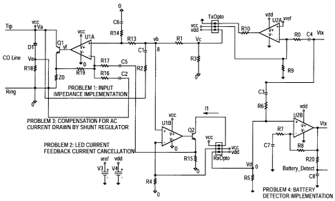
to individual unilateral transmit and unilateral receive signals. Typically,
the DAA
must also include a detector to ensure line availability and a transhybrid
balance network to cancel any transmitted signal that is reflected from the CO
line.
[004] Furthermore, inclusion of a DAA in highly integrated technology
(e.g. a PCMCIA modem) requires compact placement of components on a
CA 02486335 2004-10-29
2
printed circuit board (PCB). It is desirable that the components use a minimum
of PCB real estate and that component elevation from the PCB surface is
minimal.
[005] In reference to the DAA requirement of presenting a specific AC
input impedance to the line, this is usually accomplished by using a discrete
impedance or an active impedance block. However, the use of discrete
components conflicts with the need for compact placement discussed above
[006] Typically, optocouplers are used to provide isolation between the
device and CO line. However, optocouplers require active components (i.e.
buffers) on the line side. These active components use power isolated from the
device side circuitry. Therefore, the line side circuitry is often line
powered.
Filtering tip and ring for power usage introduces extra bulky components while
directly coupling the tip and ring to the line side circuitry introduces AC
current
feedback signals that cause distortion and noise.
[007] The problem of AC current feedback is addressed in USP
5,481,606 (Andrieu), USP 5,528,686 (Cwynar), and USP 5,946,393
(Holcombe). The solutions of Andrieu and Holcombe use a parallel current
method to eliminate feedback. The solution of Cwynar uses substantially
constant current sink amplifiers that do not generate feedback.
[008] The above-discussed prior art DAA implementations that address
current feedback suffer from extensive use of large or discrete parts. This is
also in conflict with the aforementioned goal of compact placement.
[009] Also, with reference to the requirement that the DAA must
resemble a POTS device, the prior art teaches the use of gyrators for sinking
CO line current. Such gyrators use large reactive components, or
alternatively,
introduce high distortion and add to cost and real estate.
[010] Finally, with reference to the DAA requirement of providing line
status detection, the prior art teaches the use of battery detector circuits
implemented by inserting an isolated current or voltage sensor in the current
path, thereby adding to cost and real estate.
CA 02486335 2004-10-29
3
Summary of the Invention
[011] According to one aspect of the invention, a DAA is configured to
resemble a current source for generating an AC current flow in the tip and
ring
that is proportional to the voltage thereon, with a given proportionality
constant.
The DAA therefore presents a specific input impedance to the CO line
depending on the proportionality constant of the current source.
[012] According to another aspect of the invention, feedback of AC
current on the tip and ring resulting from line side powering of isolation
optocouplers is eliminated by monitoring feedback AC current flow through the
line and generating equal and opposite current flow in the line to cancel the
feedback AC current..
[013] According to a further aspect of the invention, a shunt regulator is
used to draw or sink DC current from the line at 20 - 120 mA (depending on the
jurisdiction). Although the shunt regulator also allows AC current to flow,
the AC
current is sensed, as discussed above, and an equal but opposite phase
current is generated on the tip and ring to compensate for the AC current
drawn
by the load (i.e. shunt regulator).
[014] According to yet another aspect of the invention, DC bias current
flowing through the receive optocoupler as a result of the application of line
power, is sensed to provide a battery detect function. This eliminates the
prior
art requirement for a separate isolated battery detector.
Brief Description of the Drawings
[015] A detailed description of the preferred embodiment of the present
invention is provided herein below with reference to the accompanying
drawings in which:
Figure 1 is a block diagram of a Direct Access Arrangement
(DAA) of the prior art;
CA 02486335 2004-10-29
4
Figure 2 is a schematic diagram of a Direct Access Arrangement
(DAA) in accordance with the preferred embodiment of the invention; and
Figures 3a - 3d are schematic diagrams showing prior art line
current sink circuits.
Detailed Description of the Invention
[016] Turning to Figure 1, a prior art DAA is shown connected to the
CO line.
[017] The two-wire CO line includes a tip and ring pair that is connected
to an over-voltage protection circuit which, in tum, is connected to a
polarity
circuit (e.g. diode bridge) to define proper line polarity for the DAA
circuitry. The
purpose of the protection circuit is to prevent over-voltages from damaging
the
DAA or device.
[018] A ring detector and a battery detector are connected in parallel to
detect ringing voltage on the CO line and line availability, respectively. A
hook
switch controls on/off hook status of the DAA. A gyrator is connected to the
line
pair via the hook switch for sinking 20 - 120 mA DC current, for POTS
compatibility.
[019] A hybrid provides two-to-four-wire signal conversion between the
bi-directional line pair and unidirectional transmit (Vtx) and receive (Vrx)
lines.
Additional circuitry provides the necessary input impedance.
[020] The line side signals must be isolated from the device side.
Conventionally, transformers have been used to provide device isolation from
the CO line. A capacitor or capacitors are typically used to block the DC
voltages present on the line. Large values of transformer inductance (i.e. > 3
H)
and capacitance (i.e. 2 F) are required for good low frequency response,
resulting in increased size and added cost. The capacitor in most
configurations
must also be capable of handling high AC line voltages (caused by the ringing
signal), resulting in large capacitance size. The use of such large discrete
components is not suitable in a device where PCB real estate is limited and
CA 02486335 2004-10-29
component height is constrained. For example, for a PCMCIA standard size
card, whose components need to fit within a molded package having a total
thickness of less than 0.1" thick, it is desirable to only use small
capacitors (i.e.
< 0.1 F).
5 [021] In an effort to address the shortcomings of prior art DAAs
incorporating transformers in terms of real estate constraints and the
requirement for good low frequency response, capacitors and optocouplers
have also been used for isolation. The typical optocoupled DAA circuit is
divided into a CO line side that is not isolated and a device side that is
isolated
from the line by the optocouplers. The line side circuitry must be powered to
drive the LED of the transmit optocoupler and LDD of the receive optocoupler.
This power is typically drawn from the line. However this results in a number
of
problems such as the necessity of voltage filtering, the necessity of voltage
regulation, and the feedback of signals to the CO line.
[022] When the DAA is in an inactive (i.e. on-hook) state the line is at a
high potential (typically -48 V). During the active (i.e. off-hook) state, the
CO
line is typically at a 5 V to 12 V potential. The DAA draws a specified amount
of
current from the line (i.e. a minimum of 20 mA and up to 120 mA). Since high
AC signals are present on the line, the line signal must be filtered in order
to be
used as a clean power source. The filters and regulation circuits introduce
circuit complexity and increase the component count as well as real estate
requirement.
[023] The tip and ring (after polarity correction by the diode bridge) can
be used to provide supply voltage and ground, respectively, for the line side
circuitry. However, AC voltages on the supply must not significantly impact
the
performance of the line side circuitry. Also, the load between supply and
ground
must not result in an AC current flow from tip to ring. The CO line, without
filtering or regulation, is an acceptable power source where these two
conditions are met.
CA 02486335 2004-10-29
6
[024] The presence of AC signals on the supply gives rise to power
supply noise on the DAA amplifiers. However, this problem is overcome where
operational amplifiers having high Power Supply Rejection Ratio (PSRR) are
used. Typical operational amplifiers have high enough PSRR that this noise
does not significantly impact the transmission characteristics of the DAA.
[025] However, considerable distortion and gain variation still results
from powering the optocouplers with line power due to the feedback currents.
Existing solutions to correct this problem either require a DC holding circuit
and
a high current transistor, or require limits on amplifier selection along with
additional components.
[026] The present invention relates specifically to improvements in prior
art use of line power, input impedance and battery detection for providing
line
availability. Other aspects of the DAA shown in Figure 1 are set forth in the
prior
art literature, and therefore are not further discussed in relation to the
present
invention, unless strictly necessary to illustrate the improvements.
[027] Figure 2 illustrates an exemplary embodiment of a DAA according
to the present invention. The DAA interfaces a standard CO line having tip and
ring to an analog device via unidirectional receive (Vrx) and transmit (Vtx)
lines.
For simplification, overvoltage protection, polarity bridge, ring detect and
hook
control circuits are not shown.
[028] Electrical isolation between the CO and the device is provided by
a pair of optocouplers (TxOpto and RxOpto). In keeping with real estate
requirements for DAAs, optocouplers are normally low height components.
Each optocoupler contains a Light Emitting Diode (LED) for transmitting light
with an intensity proportional to the current traveling through the diode, and
a
Light Detector Diode (LDD). The incident light from the LED modulates the
current flowing through the LDD.
[029] One drawback of optocouplers is that the coupling between the
LED and LDD is not constant over temperature. For this reason, for every LED
in an optocoupler, two LDDs are provided wherein one of the LDDs is used to
CA 02486335 2004-10-29
7
provide feedback to compensate for the coupling variation over temperature.
This is possible since the ratio of coupling factor associated with first LDD
and
coupling factor associated with second LDD remains fairly constant over
temperature.
[030] The device (not shown) communicates via transmission Vtx and
reception Vrx lines, with the voltage bias level of the device side circuits
being
established via Vref applied to the non-inverting input of amplifier U2A.
[031] Active circuits on the CO side are powered from the tip via node
Va (CO side power Vcc) and ring via node 0 (CO side common). Active circuits
on the device side are powered by device power Vdd and device ground.
[032] The transmission circuitry of the DAA is characterized by two
operational amplifiers U2A and U1A. The inverting input of first transmission
stage (device side) amplifier U2A is connected to Vtx via capacitor C4 and
resistor RO, and connected to device ground via resistor R9. The output of
amplifier U2A is connected to the transmission LED of optocoupler TxOpto via
output resistor RIO. Diode balancing feedback is provided by the LDD
connected between the inverting input of amplifier U2A and device side power
Vdd.
[033] The first and second transmission stages are optically coupled
across the isolation barrier from the transmission LED of TxOpto to the second
LDD connected between node Vc and Vcc. Consequently, signal output from
U2A is reproduced across resistor R3 connected between node Vc and the line
side common. The voltage on node Vc (i.e. V(Vc)), is thus responsive to Vtx.
Node Vc is connected to Node Vb via resistor R1. Node Vb is connected to the
second transmission amplifier U 1 A at the non-inverting input thereof via
resistor
R13. The inverting input of amplifier U1A is connected to CO line side common
via resistor R17, capacitor C5, and resistor R15. The output of amplifier U1A
is
connected to the base of BJT Q1 base. The collector of Q1 is connected to the
tip and the emitter thereof is connected to feedback resistor R19, which is
CA 02486335 2008-03-27
8
connected to the inverting input of amplifier U1A. The emitter of BJT Q1 is
also
connected to the ring via resistor ZO.
[034] The receiver circuitry of the DAA is also characterized by two
operational amplifiers U 1 B and U2B. The non-inverting input of first
receiver
stage (CO side) amplifier U1 B is connected to Vb. The inverting input thereof
is
connected to CO line side common via resistor R4. The output of amplifier U1B
is connected to the base of BJT Q2. Node Vb is connected to the tip via
capacitor C1 and resistor R2. The BJT Q2 collector is connected to CO power
Vcc via the transmission LED of RxOpto and the emitter is connected to the
Zo junction of capacitor C5 and resistor R15. Optical feedback is provided, as
discussed above in connection with TxOpto. CO power Vcc is applied to the
inverting input of amplifier U1B via the LDD of RxOpto connected to R4.
[035] The first and second receiver stages are optically coupled across
the isolation barrier from the transmission LED of RxOpto to the LDD connected
between node Vd and Vdd. Consequently, signal output from U1 B is
reproduced across resistor R5 connected between node Vd and device side
ground. The voltage at node Vd is thus responsive to the CO line signals.
Node Vd is connected directly to the non-inverting input of amplifier U2B. The
inverting terminal of amplifier U2B is connected to device ground via resistor
R7, and capacitor C7. The output of amplifier U2B is connected directly to the
Vrx terminal of the device and via feedback resistor R8 to the inverting input
thereof. The output of U2B is also connected via resistor R20 and capacitor C8
to device ground. The node connecting R20 and C8 is connected to a battery-
detect output terminal.
[036] Since the CO line is bi-directional, signal transmissions from the
device are fed back to the device for reception, via node Vb. In order to
compensate for this feedback the transmitter (at Vtx) is coupled to the
receiver
(at Vd) via bi-directional feedback resistor R6 and capacitor C3.
[037] The DAA of the present invention incorporates a shunt regulator
from tip to ring including zener diode Dl in series with a resistor R18. The
CA 02486335 2004-10-29
9
junction of the regulator is node Ve. This node is connected to the inverting
input of amplifier U 1 A via capacitor CZ and resistor R16.
[038] The non-inverting input of amplifier U1A is connected to CO line
side common via resistor R14 and capacitor C6.
[039] One inventive feature of the DAA according to the present
invention is the elimination of AC feedback current in the line by monitoring
amount of current flowing and in response generating an equal but opposite
current flow resulting in zero net current flow. This approach eliminates the
need for a DC holding circuit and any high current transistors. Moreover there
is
no constraint requiring the use of constant current sink amplifiers, nor is
the
generation of an invariant bias voltage required. This reduces the part count,
parts complexity and real estate requirement.
[040] Operation of this feature is as follows. As shown in Figure 2, an
AC current, 11, flows from Vcc through BJT Q2 and resistor R15 to the line
side
circuit common. Hence the AC voltage across resistor R15 is 11 *RR15. The AC
voltage at the emitter of Q1 is
V(QQ1e) = -RR19/RR17 * 11 * RR15, (1)
and the AC current flow through 0 1 e is
1(QQ1e) = -RR19/RR17 * 11 * RR15/ZO (2)
This requires the current flow through the collector of Q1 to be
I(QQ1c) = ,8/(,6+1) * I(QQ1e) = - ,8/(,(3+1) * RR19/RR17 * 11 * RR15/ZO (3)
If
RR19/RR17 = I and ZO = RR15 *p/(,13+1)
Then
I(QQ1c) = -11. (5)
[041] Since AC current 11 flows from Vcc to common and AC current -
11 also flows from power Vcc to common, the net AC current flowing is zero.
[042] In addition to constraints imposed by equation (4), the values of
resistors are chosen such that enough DC current flows through the transmit
and receive LEDs for them to operate in a linear region. Since very little
current
CA 02486335 2004-10-29
is consumed by the operational amplifiers U2A, U1A, U1B, and U2B, sufficient
current is available to enhance the linearity of the optocoupler LEDs.
[043] A second feature of the DAA according to the present invention is
the incorporation of an improved transhybrid network. The AC Voltage at Vb
5 passes through the receive optocoupler RxOpto such that voltage on Vd is
equal to the voltage on Vb. The voltage on Vb comprises both the transmit and
receive signals. However, the amount of the transmit signal at Vb is known.
This is subtracted from the voltage on Vd at the device side via compensating
resistor R6, resulting in a cancellation of transmit signal at the summing
node
10 Vd. In this implementation of the transhybrid network, extra amplifier
stages are
not required.
[044] The input impedance is produced by the additional feedback path
comprising resistor R2 and capacitor Cl in conjunction with the 2nd
transmission stage (the transmission stage incorporating operational amplifier
U2A) and the ground path resistor R14 and capacitor C6. The existing
configuration taps the tip/ring voltage (the tap is the resistor network R2,
R13,
R14), and feeds it back to the 2"d stage amplifier U1A. The amplifier U1A is
configured with respect to the additional feedback as a voltage controlled
current source, where the positive terminal is the voltage input from the tap.
The resulting current, determined by the selection of feedback resistor R19
and
output resistor ZO, sources transistor Q1, largely determines AC tip/ring
current. The ultimate effect is one of apparent impedance, determined by the
ratio of tip/ring AC voltage to tip/ring AC current.
[045] For POTS compatibility, the DAA of the present invention draws
at least 20 mA and up to 120 mA of line current. By drawing the holding
current
from the telephone line, the DAA signals the central telephone office that it
is
active to either originate or complete a communications connection with the
central office (CO). The holding current is generally specified by a national
standard, which varies from one country to another in the range of 20 to 120
mA.
CA 02486335 2004-10-29
11
[046] Varying existing solutions have drawbacks, such as requirements
for large discrete capacitors or inductors, poor performance over a wide range
of frequencies, lower line termination impedance, high levels of distortion in
the
signals transmitted and received, and/or utilization of current that cannot be
used to drive other circuits.
[047] According to a further aspect of the invention, the line side
circuitry is line powered and the driving transistors are biased such that
about
20 mA of current is used when tip/ring voltage is at an operating voltage of
6V.
Hence, there is no need to activate a separate DC current sink circuit.
However,
at higher tip/ring voltages the DAA is required to draw more line current (up
to
120 mA).
[048] Zener diode Dl, in series with a resistor R18 is connected across
the tip and ring. The zener voltage is selected as the operating voltage of
the
DAA. Where the tip/ring voltage increases beyond the operating voltage, the
zener D1 conducts and a constant resistive load is present across the
tip/ring.
This resistor R18 is selected such that it draws any excess current once the
tip/ring voltage goes higher than the operating voltage of the DAA. However,
since the resistor R18 is not coupled via a coil it also presents an AC load
across the CO line. To eliminate this AC loading effect, the amount of current
flowing through R18 is sensed via a voltage tap at Ve. This tap voltage is fed
back via resistor R16 to the 2"d transmission stage (the stage based on
amplifier U2A). BJT Q1 subsequently generates an equal current but with
opposite phase such that the net AC current flow on the tip/ring is zero.
[049] As shown in Figure 2,
Ve =12 * RR18 (6)
V(QQ 1 e) = - RR 19 / RR 16 * Ve (7)
V(QQ1e) =-RR19/RR16 *12 *RR18 (8)
l (QQ1e) = -RR19/RR16 *12 *RR18/ZO (9)
I(QQ1c) =Pl(,8+1) *I(QQ1e) =-/l3/(/3+1)*RR19/RR16 *12 *RR18/Z0. (10)
Therefore if
CA 02486335 2004-10-29
12
,8/(,8+1)*RR19/RR16 *RR18/Z0= 1 (11)
Then
I(QQ1c) = -11 (as required) (12)
[050] This solution eliminates the need for large capacitors to be used.
Also there is no AC current leakage. Any AC current flow through resistor R18
is fed back to produce an equivalent opposite phase current on the line. The
use of high current transistors, high current inductors, or FETs, as shown in
the
prior art circuits of Figures 3a - 3d, with their attendant real estate
requirements
and cost, is not required. Only zener diode Dl is required to implement the DC
current sink feature of the present invention. Hence, the component count and
cost is reduced as compared to the prior art.
[051] In some communication devices (e.g. a fax machine) it is
desirable to know if a line is connected to the DAA and is available for use.
Conventionally, this is implemented by inserting an isolated current sense
device including a dedicated optocoupler, in the DAA current path. This
approach requires an extra optocoupler and a buffer for the battery detector
circuit, thereby contributing to added cost and real estate requirements.
[052] Therefore, in accordance with yet another aspect of the invention,
line availability information is transmitted through the receive optocoupler
RxOpto and, hence, a separate detector (i.e. optocoupler etc.) is not
required.
The line side is powered from the CO line, as discussed above. When the
battery voltage is present (i.e. line available), the line side circuitry is
active and
bias current flows through the receive optocoupler LED. The coupled current
through the associated LDD generates a bias voltage on node Vd. This results
in a bias voltage charging capacitor C8. The device then determines line
availability by taking the voltages across C8.
[053] The present invention, as embodied in the DAA of Figure 2,
combines an improved receive LED circuit, a transmit circuit, an input
impedance circuit, a transhybrid loss circuit, a battery detect circuit,
isolation
circuit, and a DC line current draw circuit. The described improvements
significantly decrease the component count and real estate requirements and
CA 02486335 2004-10-29
13
thereby drive the DAA cost down while maintaining or excelling the
performance of conventional designs.
[054] It will be appreciated that, although an embodiment of the
invention has been described and illustrated in detail, various modifications
and
changes may be made. The selection of resistances and capacitances may be
made by those familiar with the operating requirements of a standard DAA,
except where this disclosure provides direction. It will be appreciated that
the
aspects of the invention may be implemented separately, or cooperatively. Any
such choice of implementation may be made without departing from the sphere
and scope of the invention as described by the claims appended herein.