Note: Descriptions are shown in the official language in which they were submitted.
CA 02486394 2004-10-25
a
P105002CAlSAB
1
MULTI-PULSE CONVERTER CIRCUITS
FIELD OF THE INVENTION
The present invention relates to a multi-pulse converter circuit for
performing
conversion between an alternating current and a direct current.
S BACKGROUND OF THE INVENTION
A typical power distribution system comprises a generator connected via some
distribution network to one or more loads. The generator is typically a
multiphase
generator and the voltage output on each phase is nominally sinusoidal. If the
generator
supplies a purely resistive load then the current drawn from the generator
will also be
sinusoidal, and is also in phase with the voltage. If the generator is
connected to a load
with a significant reactive component then the relationship between the
current and
voltage becomes altered and the current starts to move out of phase with the
voltage
thereby giving rise to additional distribution losses and also de-rating the
maximum
capacity of the power source. Furthermore, if the load is non-linear then it
tends to
1 S draw a distorted current (i.e. not sinusoidal current) from the generator.
These
distortions can give rise to harmonic variations in voltage which are seen by
other loads
connected to the generator. These distortions may affect the performance of
these other
loads, as well as degrading the performance of the power supply system. Thus
it is well
known that it is desirable to keep harmonic distortion low.
Aeronautical systems represent a particular challenge to control of harmonic
distortion.
This is because in some modern aircraft the generators typically operate over
a wide
frequency range, and thus methods of reducing harmonic distortion using
filters that
work well with fixed frequency systems cannot be used in aeronautical systems.
Furthermore, many of the flight surfaces may be electrically actuated and
these
2S actuators can by virtue of their variable speed drives or power supply
arrangement
impose significant non-linear electrical loads. Finally, solutions for
providing control of
harmonic distortion often involve the use of transformers. These transformers
have to
be rated to be able to handle the maximum power that is to be transferred
across them
CA 02486394 2004-10-25
2
together with an acceptable margin of safety. Transformers capable of handling
large
amounts of power tend to be relatively heavy.
Variable speed controllers and DC converters are often based on a three phase
bridge
circuit, an example of which is shown in Figure S. Such a bridge circuit is
also known
as a 6 pulse bridge because there are six pulses per cycle - this being formed
on one per
half cycle for each of the three phases.
In theory a six pulse bridge circuit produces current harmonics at 6n+ 1 and
6n- l,
where n is an integer, i.e. at 5, 7, 11, 13, 17, 19 and so on times the
fundamental
frequency. Also the magnitude of each harmonic is approximately a reciprocal
of its
harmonic number. Consequently there would be 20% fifth harmonic, 14% seventh
harmonic, 9% eleventh harmonic and so on.
In principle there are no even-order harmonics because the bridge circuit is a
full wave
rectifier.
SUMMARY OF THE INVENTION
According to a first aspect of the present invention there is provided a
converter circuit
for converting between an alternating current (AC) supply and a direct current
(DC)
load; the converter circuit comprising:
a first semiconductor bridge circuit having first and second DC rails, and a
plurality of AC rails for connection to an AC bus;
at least one further semiconductor bridge circuit having first and second DC
rails and a plurality of AC rails;
at least one phase shifting device; and
a harmonic injector,
wherein the or each phase shifting device interconnects an associated one of
the
further semiconductor bridge circuits to the AC bus, the semiconductor bridge
circuits
are connected in series, the harmonic injector is responsive to a harmonic
signal
developed across at least one of the semiconductor bridge circuits and uses
this to form
a signal which is used to reduce harmonic interference in the AC bus.
CA 02486394 2004-10-25
3
In order to ensure that the current mismatches give rise to the generation of
repetitive
waveforms across each semiconductor bridge circuit there are no current paths
that are
completely individual to any one of the bridge circuits. Thus there are no
components,
such as DC filtering/smoothing capacitors, connected solely across the output
of the
individual semiconductor bridge circuits. Where series connected capacitors
form a
chain of capacitors between the positive and negative DC output rails of the
converter
circuit such that a "central node" is formed, any connection between the
central node
and a node between the first and second semiconductor bridges is via a shared
path and
via at least one intermediate component. The intermediate component is
advantageously part of the harmonic injector.
Preferably the AC supply is a three phase supply.
Preferably the converter circuit is a rectifier for converting an AC supply to
a DC
supply. The AC supply need not be at a fixed frequency as the rectifier
circuit is
suitable for use with variable frequency AC supplies. Preferably each
semiconductor
bridge circuit comprises, for each individual one of the AC supply rails, a
pair of
semiconductor devices in series connection between the first and second DC
rails with
their associated AC supply rail being connected to the node formed by the
interconnection between the pair of semiconductor devices.
Advantageously the at least one phase shifting device comprises a transformer.
A three
phase transformer having its secondary windings connected in a delta
configuration is
well known in the art for the generation of a 30° phase shift. However
other
transformer configurations, such as star or delta configurations in which
components of
other windings are added into a secondary winding current path, see for
example the
winding schemes proposed by Georges - Emile April and Guy Olivier, "A Novel
Type
of 12 Pulse Converter" IEEE Transactions on Industry Applications Vol. lA -
21, No.l,
1985.
CA 02486394 2004-10-25
4
Preferably the connections from the AC supply to the phase shifting device and
the first
semiconductor bridge circuit are in series. This ensues that an equal current
balance, or
a predetermined current balance, can be forced in each bridge circuit.
In a preferred embodiment each of the primary windings of the or each
transformer
forming the or each phase shifting device is in series with a respective input
of the first
bridge circuit. However, in a further embodiment of the present invention the
AC
supply paths to at least two of the semiconductor bridges are in parallel.
The inventors have noted that by connecting the AC supplies to inputs to the
semiconductor bridges in series, and by connecting the outputs of the
semiconductor
bridge circuits (which form three phase rectifier circuits) in series, but
with a capacitor
filter being connected across the series combination of the bridge circuits
rather than
solely across each individual bridge circuit then the instantaneous mismatch
of output
currents from the bridge circuits causes repetitive bypass paths to be formed
through the
diodes of the bridge circuits for the excess currents. This causes a voltage
collapse on
one bridge and a corresponding voltage on the other bridge (and vice versa)
and results
in individual bridge circuit output voltages that are repetitive waveforms,
and in
particular are signals in the form of unidirectional square waves at six times
the supply
frequency rather than constant voltage levels. The square waves are
complimentary and
sum to a constant direct voltage level across the series connected arrangement
of bridge
circuits, as seen at the capacitor filter. In embodiments where P
semiconductor rectifier
bridges are connected in series a square wave is developed across each bridge
with a
period of '-'-n .
In a first embodiment having only a first and second semiconductor bridge
circuits the
harmonic injector is interposed between the first and second semiconductor
bridge
circuits. Preferably the harmonic injector is a passive device that is
responsive to the
current mismatch produced between the semiconductor bridge circuits. In a
preferred
embodiment of a rectifier unit the harmonic injector comprises a transformer
having a
first winding herein known as the injection winding connected to one of the
bridge
CA 02486394 2004-10-25
circuits such that the transformer is responsive to the harmonic signal
developed across
the bridge circuit. A second winding herein known as the sensing winding of
the
injection transformer is connected to the AC terminals of a rectifier block,
and the DC
terminals of the rectifier block are connected between the first and second
5 semiconductor bridges. Using this circuit arrangement, the turns ratio of
the insertion
transformer can be chosen to optimise the level of harmonic injection. In
addition the
normal AC and DC side voltage and current relationships are preserved such
that the
circuit components may be optimised and undesirable effects for example
transformer
saturation, are prevented. The deliberate injection of harmonic components
having a
selected harmonic order number and phase can be used to cancel or minimise
other
harmonic components which are inherently generated during the rectification
process
thereby reducing harmonic distortion of the current drawn by the rectifier.
In other embodiments of the invention, part of the harmonic injector may be
connected
between the "central node" formed between the filter capacitors and a node
located
between the semiconductor bridge circuits, whereas other components of the
harmonic
injector may be either in series with the semiconductor bridge circuits or in
parallel with
the series connected semiconductor bridge circuits.
According to a second aspect of the present invention there is provided a
method of
reducing total harmonic distortion arising from an AC to DC converter, the
method
comprising: providing first and second three phase passive rectifiers in
series, with the
second rectifier being supplied via a delta connected transformer and the
first rectifier
being supplied by connection to a star connected transformer or via series
connection to
the primary windings of the delta connected transformer, and wherein a common
current path is provided through the first and second rectifiers such that
instantaneous
current conflicts cause the creation of "by-pass" current paths through one or
other of
the rectifiers giving rise to the generation of a waveform at six times the
supply
frequency which is used to drive an harmonic injector compensation circuit for
injecting
a harmonic waveform at a node between the first and second rectifiers.
CA 02486394 2004-10-25
6
BRIEF DESCRIPTION OF THE DRAWINGS
The present invention will further be described, by way of example, with
reference to
the accompanying drawings, in which:
Figure 1 schematically illustrates a twelve pulse transformer based multiphase
rectifier
S of the type known in the prior art;
Figure 2 schematically illustrates a further prior art twelve pulse rectifier
wherein
galvanic isolation has been dispensed with in order to eliminate one of the
transformers
compared to the arrangement shown in Figure 1;
Figure 3 shows a further prior art AC to DC converter;
Figure 4 schematically illustrates an AC to DC converter having series
connected
rectifier bridges;
Figure 5 illustrates a rectifier bridge in greater detail;
Figure 6 illustrates the individual current contributions through the upper
diodes in the
rectifier bridge shown in Figure 5 together with their sum;
Figure 7 schematically illustrates the current flow paths in a pair of series
connected
rectifier bridges of the type shown in Figure 5;
Figure 8a to 8f show various waveforms relating to the operation of the
circuit shown in
Figure 7;
Figure 9 schematically illustrates a rectifier constituting an embodiment of
the present
invention;
Figure 10 schematically illustrates a rectifier constituting a further
embodiment of the
present invention;
CA 02486394 2004-10-25
7
Figure 11 is a plot of total harmonic distortion versus turns ratio of the
injection
transformer in Figure 9;
Figures 12a to 12d show voltage waveforms at various points within the circuit
shown
in Figure 4;
Figures 13a to 13c shows the improvement in equivalent waveforms with the
embodiment of the present invention illustrated in Figure 9;
Figure 14 shows a further embodiment of the present invention;
Figure 15 shows a current waveform for the circuit of Figure 9;
Figure 16 shows a further embodiment of the present invention in which part of
the
harmonic injection circuit has been placed in the DC output rail of the
converter;
Figure 17 shows a further embodiment of the present invention in which the AC
inputs
are in parallel;
Figure 18 shows a further embodiment of the present invention;
Figures 19a to 19i schematically illustrates voltage waveforms occurring at
various
points within the circuit shown in Figure 18;
Figure 20 is a graph showing harmonic distortion versus injection transformer
turns
ratio for the circuit shown in Figure 19;
Figure 21 is a circuit diagram of an embodiment of the present invention
utilizing
current injection and voltage injection;
Figure 22 schematically illustrates the interrelation between the current
injection and
voltage injection waveforms; and
CA 02486394 2004-10-25
Figures 23a to 23i shows waveforms in the converter circuit shown in Figure
21.
DESCRIPTION OF PREFERRED EMBODIMENTS OF THE INVENTION
The arrangement shown in Figure 1 is that of a prior art twelve pulse
rectifier. A three
phase supply comprising phase A having a voltage VA and a current IA and
phases B
and C similarly designated are supplied to star connected windings 2, 4 and 6
of a
transformer generally designated 8. It is common for the phases to be referred
to as
"red", "yellow" and "blue", and designated by R, Y and B respectively where
red is the
zero phase, yellow is the 120° phase and blue is the 240° phase.
Both conventions will
be used here with A = red, B = yellow and C = blue. The transformer has two
sets of
secondary windings. A first set of windings 10, 12 and 14 are also connected
in a star
configuration, i.e. the windings are connected to a common node 16 and for
simplicity
may be referred to as a "star" windings 17. Outputs of the windings 10, 12 and
14 are
supplied to a first rectifier assembly 20 which has the configuration shown in
Figure 5.
A second set of windings 22, 24 and 26 are connected in the delta
configuration and for
simplicity may be referred to as "delta" windings 27. Outputs from the delta
connected
windings 27 are supplied to a second rectifier block 28 whose construction is
the same
as the rectifier block 20. It is well known that, and can also be shown by
graphical
analysis, that the delta configuration in which each winding forms the
difference
between two of the input phases, for example VA - VB, Va - V~, or V~ - VA
results in
the generation of further sinusoids 30° out of phase with the input
sinusoids. In order to
maintain the correct current and voltage relationship between the primary and
secondary windings the relative turns ratio must be 1:1 for the star windings
and
1: ~~ 3 for the star-to-delta windings. T'he transformers can also be
configured for step up
or step down action.
The rectifier units 20 and 28 are connected in parallel and the positive
output rails 30
and 32 are provided as inputs to an inter-phase reactor 34, which is required
to ensure
instantaneous current balance between the two rectifier units.
CA 02486394 2004-10-25
9
Whilst this arrangement works adequately to give harmonic cancellation of the
5th and
7th order harmonics the input transformer 8 has to be rated to carry the
entirety of the
power requirement of the load connected to the rectifier together with some
suitable
margin of safety. This impacts on the gauge of the transformer windings and
the weight
S and size of the device in general.
Figure 2 shows a further prior art arrangement described by Derek A Paice in
his book
titled "Power Electronic Converter Harmonics - Multi-pulse Methods for Clean
Power".
This arrangement, taken from Figure 5-16 of the book shows that the
arrangement
shown in Figure 1 can be simplified by dispensing with the star connected
transformer
and connecting the primary windings 2, 4 and 6 directly to respective inputs
34, 36 and
38 of the first rectifier block 20. This results in a reduction of the power
handling
requirements of the transformer 8 but simultaneously also results in the loss
of galvanic
isolation between the input supplies VA, VB and V~ and the DC output bus 40.
In each of these prior art arrangements the DC rectifier blocks are connected
in parallel
and the output of each is held at the DC output voltage of the rectifier by
virtue of being
coupled to a smoothing capacitor, for example as shown in Figure 1.
The inventors have realised that the apparently minor reconfiguration of the
circuit
achieved by placing the outputs of the converter blocks in series whilst
simultaneously
placing their inputs effectively in series and removing individual voltage
smoothing
capacitors from around the blocks results in a radically different mode of
operation, in
which conflict between the bridges can be used to self generate a waveform for
harmonic cancellation.
The paper "A New High-Pulse Voltage Sourced Converter for HVdc Transmission" Y
H Liu, J Arrillaga and N Watson, IEEE Transactions on Power Delivery Vol. 18,
no. 4,
October 2003, pages 1388 - 1393 discloses a re-injection converter as shown in
Figure
3. In order to simplify the discussion of the Figure like reference numerals
will be used
to refer to items which have already been described with respect to Figures 1
and 2.
Thus star winding 17 is connected to a first rectifier block 20 and delta
winding 27 is
CA 02486394 2004-10-25
connected to a second rectifier block 28. The rectifier blocks 20 and 28 are
arranged in
series. The rectifier block 28 has capacitor 40 in parallel with it, whereas
capacitor 41
is in parallel with the rectifier block 20. An "H" bridge composed of four
silicon
controlled rectifiers 42-45 (active switches) which are electronically
controlled to be
5 either conducting or non-conducting is connected between the DC output
rails.
Switches 42 and 44 are connected in series, as are switches 43 and 45. A
common node
for switches 42 and 43 is connected to the positive DC rail. A common node of
the
switches 44 and 45 is connected to negative DC rail. A primary winding of a
transformer 46 is connected between the opposing sides of the H bridge. A
secondary
10 winding of the transformer is connected between a midpoint between the
rectifiers 20
and 28, and a common node between the capacitors 40 and 41.
In use, the switches 42 to 45 are switched so as to derive a re-injection
voltage U~ which
is imposed upon the node 48 between the rectifier bridges. The switches can be
controlled either to:
a) short circuit the primary winding of the injection transformer;
b) connect the primary winding in a forward direction;
c) connect the primary winding in a reverse direction;
as set out in column 2 on page 1388 of the IEEE Journal.
Short circuiting the transformer primary requires the use of active devices,
(in
conjunction with commutation diodes) in order to ensure that switches 42 and
43, or
switches 44 and 45 are simultaneously conducting in order to short circuit the
transformer primary winding whilst avoiding shorting the DC rails together.
This
arrangement requires the provision of a controller to control the operation of
each of the
active switches and introduces a potentially damaging failure mode in which
series
connected switches could both be turned on or fail on, thereby shorting the DC
output
rails together. This circuit operates in a significantly different way to the
present
invention.
Figure 4 schematically illustrates an AC to DC converter whose operation will
be
considered so as to exemplify the generation of conflict between the bridges.
As
CA 02486394 2004-10-25
11
before, the three phase supply is schematically represented by voltage sources
VA, VB
and V~ which nominally have the same output voltage but which are displaced in
phase
with respect to one another by 120°. Voltage supply VA is connected by
way of a first
primary winding 50 of transformer 51 to a first input 52 of a first rectifier
bridge
generally designated 54 having first and second DC rails SSa and SSb.
Similarly the
voltage supplies VB and V~ are connected by way of respective transformer
primary
windings 56 and 58 to input connections 60 and 62 of the bridge 54. Each
supply VA,
VB and V~ is shown as being in series with a respective inductor LA, LB and L~
which
could be an individual component but which may be present simply as a result
of self
inductance of the conductors used to interconnect the three phase supply to
the rectifier
and/or the leakage inductance of the transformer 51. The winding 50 is
magnetically
coupled via transformer action with the corresponding secondary winding 70,
primary
winding 56 is magnetically coupled to corresponding secondary winding 72, and
primary winding 58 is magnetically coupled to corresponding secondary winding
74,
and the windings 70, 72 and 74 are connected such that each is in series with
the others
and a connection point is made at each node between the windings. Thus the
windings
70, 72 and 74 are connected in a delta configuration. A connection is made
from a first
node 76 between windings 72 and 74 to a first input 78 of a second rectifier
bridge
circuit, generally indicated 80 having first and second DC rails 81 a and 81
b. A
connection is made from a second node 82 between windings 70 and 72 to a
second
input 84 of the rectifier 80, and a connection is made from a third node 86
between
windings 70 and 74 to a third input 88 of the second rectifier 80.
The windings 50, 56 and 58 are placed in series connection with the inputs 52,
60 and
62 of the first bridge 54 and this has the consequence that a predetermined
relationship
is established between the currents in the first and second rectifier bridges
54 and 80.
By choosing a primary to secondary transformer ratio of 1/.~ the rectifier
bridges are
fed with the same current amplitude, but the phase difference between them is
30°. Any
instantaneous current imbalance results in a "conflict" which can only be
resolved by
the generation of "by-pass" paths within one or other of the bridges.
CA 02486394 2004-10-25
12
In order to appreciate the working of the present invention it is advantageous
to
consider the operation of each individual rectifier bridge in greater detail.
The rectifier
bridge is shown in greater detail in Figure 5 and is of a 6 pulse design. The
bridge
comprises positive and negative rails 100 and 102, respectively.
Interconnecting the
rails 100 and 102 are three pairs of diode rectifiers. The diodes in each pair
are in series
configuration and each pair rectifies a respective phase of the multiphase
supply. Thus
the first diode pair 104 comprises diodes 106 and 108. The anode of diode 106
is
connected to the negative rail 102 and the cathode of the diode 106 is
connected both to
an input terminal P1 for accepting a first input phase, but also to a anode of
the second
diode 108. The cathode of the second diode 108 is connected to the positive
supply rail
100. A second diode pair 110, comprising diodes 112 and 114, is similarly
connected,
but this time to supply P2, and a third diode pair 116 comprising diodes 118
and 120 is
similarly connected to supply P3.
For simplicity, we shall consider the sum of the currents flowing in diodes
108, 114 and
120 resulting from the positive half cycles of the supplies Pl, P2 and P3. It
will be
appreciated that similar analysis can be done for the diodes 106, 112 and 118
during the
negative half cycles P1, P2 and P3.
Figure 6 schematically illustrates the current flowing in diode 108 from
supply P1,
current flowing in diode 114 from supply P2 and current flowing in diode 120
from
supply P3. It can be seen that the conduction period of diode 108 connected to
supply
P 1 commences approximately 120° before the conduction period of
diode 114
connected to supply P2, which in turn is 120° in advance of the
conduction period of
diode 120 connected to supply P3. When a diode is forward conducting the
voltage
drop across it falls to one diode drop, i.e. approximately 0.7 volts, and thus
when two
diodes are conducting simultaneously then to a first approximation their
respective
supplies are effectively connected together. Thus during the period TA shown
in Figure
6 when diodes 108 and 114 are both conducting supply P 1 is effectively
shorted to the
positive supply rail 100, and supply P2 is also effectively shorted to the
positive rail
100.
CA 02486394 2004-10-25
13
The total current flowing through the rectifier during the positive half
cycles is the sum
of the currents flowing through diodes 108, 114 and 120. Either numerical or
graphical
analysis shows that the sum of the currents can be considered as a DC value
with a
ripple current occurring at six times the fundamental frequency of the input
supplies.
The above analysis holds true for the currents flowing in each of the bridges
54 and 80.
That is each bridge rectifies the associated three phase supply to produce an
output
current of the type shown in Figure 6 comprising a DC component with a ripple
component where the ripple has a fundamental frequency of six times the input
supply
frequency. Thus the peaks in the ripple current are displaced at 60°
intervals with
respect to the input currents. However it will also be noted that the input
currents to the
bridges in Figure 4 are displaced by 30° with respect to one another by
virtue of the
delta transformer action. Thus the peak ripple current in one bridge coincides
with the
minimum ripple current in the other bridge. Thus the instantaneous bridge
currents
resulting in their rectification action are generally different. However the
bridges have
1 S been connected in series (both at their input side and their output side)
and consequently
the same current is forced to flow in each bridge.
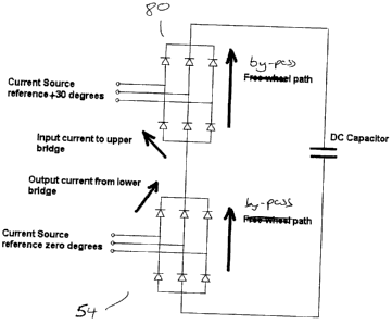
Referring to Figure 7, it can be seen that the output current from the lower
bridge 54
flows as an input current to the upper bridge 80. Considering an instant in
time in
which the current provided by the lower bridge 54 is greater than the current
provided
by the top bridge 80, excess current forces its way through the upper bridge
by opening
up a bypass path through the serially connected diodes. The emergence of a
bypass
path causes one of the diode pairs to switch on. From this it follows that the
voltage
difference across the upper bridge assembly collapses to approximately zero.
When a
bypass path is opened all of the output voltage appears across the lower
rectifier bridge
assembly. However, due to the periodic nature of the ripple current the
current
originating from the upper diode bridge increases and that originating from
the lower
diode bridge decreases such that after '/12 of a cycle of the AC input
waveform the
upper diode bridge now wishes to pass more current than the lower diode bridge
and as
a consequence the bypass path of the upper diode bridge closes and a bypass
path in the
lower rectifier block opens. Thus the voltage difference across the lower
rectifier block
CA 02486394 2004-10-25
14
collapses to substantially zero and substantially the entirety of the output
voltage now
appears across the upper rectifier block.
It can therefore be seen that each rectifier block has a square wave voltage
appearing
across it having a frequency which is six times the input frequency and a
magnitude
which is the entirety of the output voltage (the voltage drop across a diode
to turn it on
will be ignored as it is insignificant). The square waves occurring across the
upper and
lower rectifier bridges are in anti-phase and automatically passively
synchronise with
the input frequency.
Figure 8a shows the current Ii which results from rectification of the AC
input current
to the first (or lower) rectifier block 54, whereas Figure 8b shows the
current IZ which
results from the rectification of the AC input currents to the second (or
upper) rectifier
block 80. Figure 8c shows the sum of these currents as a function of time.
Figures 8d
and 8e show the by-pass current (i.e. the current difference between Ii and
I2) in the
lower and upper rectifier blocks 54 and 80, respectively. Figure 8f shows the
voltage
Vo, developed across the first (lower) rectifier block 54.
The described current mismatches can be utilised to control the generation of
harmonic
components that are to be injected into the system in order to cause
destructive
harmonic interference and thereby reduce the total harmonic distortion in the
current
waveforms drawn from the three phase generator. For many applications adequate
harmonic compensation can be achieved through the use of passive components
acting
on the current mismatch, thereby providing a relatively inexpensive and yet
reliable
system.
Figure 9 schematically illustrates a rectifier constituting an embodiment of
the present
invention wherein a harmonic injector circuit, generally designated 140,
comprising a
harmonic injection transformer 150 and an associated diode bridge 152 is
interposed
between the first rectifier bridge 54 and the second rectifier bridge 80. The
diode
bridge 152 comprises four diodes D 1 to D4 arranged to form a full wave
rectifier. The
diodes D 1 and D2 are in series, as are D3 and D4. The anodes of diodes D2 and
D4 are
CA 02486394 2004-10-25
connected together forming a first DC terminal DC 1. Similarly the cathodes of
diodes
D1 and D3 are connected together, forming a second DC terminal DC2. A first AC
terminal, AC 1, is defined by the node between diodes D 1 and D2, whereas a
second AC
terminal, AC2, is defined by the node between diodes D3 and D4. An injection
5 winding 151 of the injection transformer 150 is connected between the
positive supply
rail 100 of the first rectifier bridge 54 and a virtual ground 154. The
virtual ground 154
is formed by first and second series connected capacitors 160 and 162
connected
between DC output rails 164 and 166. The capacitors provide a high impedance
to the
DC voltage but a low impedance path to the AC mismatch current that flows in
the
10 injection winding 151. It has been noted in this circuit there is an
instantaneous
mismatch of the output currents from each bridge which causes repetitive
bypass paths
to be formed and each bridge output voltage is an unidirectional square wave
at 6 times
the supply frequency. The harmonic injector circuit is used to provide the
mismatch in
bridge currents at carefully chosen periods of time. This is controlled by the
injection
15 transformer turns ratio and gives a simple and automatically scaled control
mechanism
which is used to alter the formation of the bridge bypass paths. This has the
desirable
effect of altering both the unidirectional square-wave bridge output voltages
and
corresponding AC side converter terminal voltages such that the harmonic
components
of voltage and current are minimised.
The sensing winding 156 carries an alternating current waveform with a peak
value
equal to the DC load current, however the corresponding voltage across winding
156 is
very low by virtue of the required turns ratio and gives a resultant
transformer VA
rating that is very low compared to the throughput power of the overall
rectifier system.
Figure 10 shows an alternative embodiment of the invention where the primary
winding
is now connected to one of the AC terminals of the injection diode bridge 152
rather
than to the positive rail of the first bridge 54. Otherwise the mode of
operation remains
essentially unchanged. However the circuit shown in Figure 10 gives output
waveforms
with better symmetry and hence represents an improvement over the circuit
shown in
Figure 9.
CA 02486394 2004-10-25
16
Other possible connections exist, for example the injection winding may be
connected
to the negative rail. Thus the "direction" of the injection winding with
respect to the
sensing winding may be reversed. Additionally, compared to Figure 10, the
direction of
both the injection and sensing windings may be reversed. The connection to the
injection winding can be made to either the positive rail of semiconductor
bridge 54 or
to the negative rail of semiconductor bridge 80. These alternative possible
arrangements can be implemented singly or in combination
Figure 11 shows a graph of the total harmonic distortion of the AC terminal
voltage of
the converter (shown at points R, Y, B of Figure 10) as a function of the
injection
transformer turns ratio N. It can be seen that a minimum total harmonic
distortion
occurs with a turns ratio of approximately 14, although it can also be seen
that the
circuit is relatively insensitive to small variations from this value. In this
context the
turns of ratio N =14 = V' . The input current total harmonic distortion also
depends on
s
the value of the input inductors interposed between the idealised voltage
generators and
the windings 50, 56 and 58.
It will be appreciated that the closer the voltages and currents drawn from
the supply
approximate a single sinusoid then the better the performance of the supply
will be with
regard to harmonic distortion.
It is worth comparing the voltage and current waveforms of the circuit shown
in Figure
9 with those of the circuit shown in Figure 4.
Figure 12a shows the voltage waveform V~ between point Rl and virtual ground
154
in the circuit of Figure 9. As used herein the rectifier 54 may be referred to
as the first
rectifier or the lower rectifier and waveforms associated with it may include
the
subscript "1" or "L". Similarly the rectifier 80 may be referred to as the
second or
upper rectifier and waveforms associated with it may include the subscript "2"
or "U".
A square wave shape as indicated by waveform 200 with peak values of~
2° where Vo
is the rectifier output voltage. In order to refer the point Rl to the neutral
point N, zero
CA 02486394 2004-10-25
17
sequence components 202 which mathematically can be shown to be the average of
the
red phase voltage V~,o and equivalent voltages on the yellow and blue phases
i.e.
V~G + V,z~ + VBLG need to be subtracted from V~,G, to give V~,N as shown in
Figure
3
12b. We then need to add the voltage reflected across the transformer S 1
resulting from
the voltage difference between nodes 76 and 86 in Figure 4, and as shown in
Figure
12c. The sum of these contributions gives a step wise approximation between
measuring point R and neutral as shown in Figure 12d.
However, in the circuit shown iwFigure 9 the action of the harmonic injection
circuit is
to modify V~,N as shown in Figure 13a. Similarly the voltage reflected back
across the
transformer S1 is also modified by as shown in Figure 13b to give a voltage V~
in
Figure 13c is a 24 pulse stepped waveform which is a much better approximation
to a
sinusoid than the 12 pulse prior art voltage shown in Figure 12d.
Figure 14 shows a variation of the circuit of Figure 9 whereby two
transformers are
used. The circuit operates in an identical manner but enables the DC output
voltage to
1 S be varied and also provides galvanic isolation.
A 15 kW prototype has been built and tested by the applicant using either the
inherent
transformer leakage inductance and the input inductors or additional external
inductors
having a value of 100 ~H to represent the source and cable inductance of a
typical
installation. Under both circumstances the total harmonic distortion obtained
remained
below 2%. Figure 15 shows the three phase current waveforms drawn by the
rectifier
from the three phase generator using the circuit shown in Figure 9 and loaded
to 15 kW.
Furthermore during the test the injection transformer was confirmed to have a
power
rating of 2% of the main converter rating. Furthermore, since the injector
transformer
operates at six time the fundamental frequency it has the characteristics of a
high
frequency magnetic component and hence the reduced physical size.
In each of the preceding embodiments harmonic cancellation has occurred by
virtue of
injecting current between the rectifier bridges. The current injection circuit
can also be
CA 02486394 2004-10-25
18
implemented in different ways. In the configuration represented in Figure 16,
the
sensing winding 156 winding and its associated diode bridge have been moved
from the
mid-point of the rectifiers (semiconductor bridges) 54 and 80 to the positive
terminal or
positive rail. It could have equally been placed in the negative
terminal/rail. The
optimum turns ratio N for the arrangement shown is in the region of 14.
The sensing winding could also be spread into several windings and distributed
across
the circuit, i.e. a second diode bridge and winding are inserted in the
negative rail, with
the polarity of the diodes reversed to give mirror injection circuits. The
optimum turns
ratio for this circuit is in the region of 28.
Another possibility could also involve connecting the primary winding (which
can also
be thought of as an injection winding to the secondary or sensing winding
using a tap in
the sensing winding.
Figure 17 shows a further embodiment of the present invention in which, as
with the
embodiments shown in Figures 9 and 10 a harmonic injection transformer 150 and
its
associated rectifier bridge 152 is disposed in series connection in between a
first
rectifier bridge 54 and the second rectifier bridge 80. A DC output from the
rectifier is
developed across rails 220 and 222 and smoothed by a split storage capacitor
arrangement 224 in which a capacitor is centre tapped to ground. The first
bridge 54
has its AC input terminals connected directly to the polyphase AC supply. The
phase
shifter in the form of a star delta transformer 230 also has its primary
windings
connected to the polyphase AC supply. Thus, the input sides of the
semiconductor
bridges 54 and 80 are connected in parallel whereas the bridges themselves are
connected in series. However, unlike the earlier embodiments, a squarewave
voltage
waveform is not developed across the bridges because current balancing can
occur by
virtue of the parallel connected input arrangements. Thus each bridge develops
a DC
voltage across it upon which is superimposed a ripple at six times the
fundamental
frequency. The ripple current as seen by the injection transformer 150 is
transformed
and re-injected back via the diode bridge 152 thereby generating ripples at
twelve times
the input frequency such that these can engage in harmonic cancellation. The
CA 02486394 2004-10-25
19
magnitude of the ripple occurring across the semiconductor bridge 54 is much
less than
the magnitude of the equivalent square wave in the earlier embodiments of the
invention and hence the transformer ratio needs to be modified. Initial work
suggests
that the transformer ratio should have a one to two times step up ratio with
initial
indications indicating that a step up ratio of about 1.5 gives adequate
results.
Figure 18 shows a further embodiment of the present invention. This is similar
to the
arrangement shown in Figure 4 and hence a current mismatch occurs between the
rectifier bridges 54 and 80 that gives rise to the generation of a
substantially square
wave voltage at six times the input frequency. A harmonic injector, generally
designated 290 comprises a transformer in combination with a full wave
rectifier. The
transformer 300 is connected such that one end of its primary or injection
winding 301
is connected to a node 302 directly between the rectifier bridges 54 and 80.
The other
end of the injection winding is connected to a node 304 between a pair of
capacitors
306 and 308 which are connected between a positive DC rail 310 and a negative
DC rail
312.
A secondary or sensing winding 320 has a first connection made to a node 322
between
a pair of series connected rectifiers 324 and 326. A second connection is made
to a
node 328 between series connected rectifiers 330 and 332. The rectifiers are
diodes.
The cathodes of diodes 326 and 332 are connected to the positive rail 310 and
the
anodes of diodes 324 and 330 are connected to the negative rail 312. Typically
the
transformer 300 is rated to about 2% of the power throughput.
In the earlier examples of the invention the current conflict in the rectifier
bridges gave
rise to a square wave voltage being developed across the bridges. In this
embodiment
the same process is still at work, and the current mismatch between the series
connected
rectifiers causes a current flow through the injection winding of the
transformer to the
node between the capacitors 306 and 308 which serve to block a DC current path
but to
permit an AC flow.
CA 02486394 2004-10-25
The transformer action couples the current flow across to the diodes 324, 326,
330 and
332. Each diode can only be either non-conducting or conducting. When a diode
is
conducting the voltage drop across it is close to zero volts. Consequently the
secondary
transformer can be thought of being connected to the DC supply either in one
direction
5 when for example diodes 326 and 330 conduct or in the other direction when
diodes
324 and 332 conduct.
The transformer action from the transformer 300 causes a voltage change to be
imposed
on the node 302 and this in turn is imparted onto the AC supply via the
windings 70,
72, 74 and 50, 56 and 58 of the supply transformer. Thus a square wave voltage
V;~~, at
10 six times the supply frequency is injected between the midpoint of the
rectifier (e.g.
node 302) and the midpoint of the output filtering capacitors.
The injection of this voltage creates complementary stepped waveforms at the
output of
the main rectifiers, which are implemented as semiconductor bridges, 54 and 80
which
result in 24-pulse shaped waveforms at the right hand side of the input
inductors 340,
15 342 and 344 (i.e. the side remote from the AC generator).
The injected voltage is added to the output voltage of the upper rectifier
bridge 80, and
subtracted from the output voltage of the lower rectifier bridge 54. Therefore
the output
voltages of the main rectifiers are given by:
Vo, = V~ + V;~~ (1)
V
20 Voz = ~ - V~; (2)
where Vol is the voltage across the lower rectifier bridge 54 and Vo2 is the
voltage
across the upper rectifier bridge 80.
When the output current provided by the lower rectifier bridge 54 is greater
than the
output current provided by the upper rectifier bridge 80, the imposed
injection current
CA 02486394 2004-10-25
21
I;"~ is negative. Due to the amp-turns balance in the transformer, a negative
current will
flow in the sensing winding 320 which will bring diodes 332 and 324 into
conduction.
Consequently, a voltage of Vo will be imposed across the sensing winding, and
will be
reflected to the injection winding as ~° , where N is the injection
transformer turns
S ratio N = NS where Ns is the number of turns in the sensing winding and Ni
is the
N;
number of turns in the injection winding. Therefore the output voltages across
the main
rectifier blocks will become:
v°~ ° v~y+ N) ~3)
v°Z - viC~_ N) ~4>
When the output current of the upper rectifier 80 becomes greater than the
output
current of the lower rectifier 54, the injection current reverses and the
insertion voltage
becomes negative and of the same magnitude. Since the output currents of the
rectifiers
are phase-shifted by 30°, both the injection current and voltage are
synchronised to them
and have a frequency of six times the supply frequency.
Figure 19 shows how the modification of the Vol and Vo2 waveforms to
complementary mufti-level stepped shapes results in a 24-pulse shaped waveform
at the
right hand side of the input inductors.
Figures 19a, b and c first shows the input voltages of the lower rectifier 54
with respect
to the mid-point of the output DC link, V~,G, VLL,o and VBr.G respectively. In
the
convention used herein the subscript 'L' refers to the lower rectifier 54 and
the
subscript 'U' refers to the upper rectifier 80. When the input current Ice, is
negative,
diode 360 of the RL leg conducts and the V~,G voltage equals -Vo/2. When the
input
current becomes positive, the terminal RL is connected to the positive
terminal rail of
the lower rectifier block 54 by diode 362 becoming conductive, and the voltage
V~,G
CA 02486394 2004-10-25
22
equals the injection voltage V;"~. The waveforms V~ and VBLG are identical to
V~,G
but phase-shifted 120° and 240° respectively.
The common mode voltage VNG shown in Figure 19d is then determined using
equation
(S),
S VNG = V nt,c + Vmc + V a vc (S)
3
allowing the calculation of V~,N, since V~,N = V~,G - VNC. V~,N is shown in
Figure
19e.
The VRUG and VBUG input voltages to the upper rectifiers are shown in Figures
19f and
19g. When the input current IRU is positive, the Ru input terminal becomes
connected to
the positive output of the converter by virtue of diode 364 switching on and
consequently the voltage VRUG equals 2° . When the input current IRU
becomes
negative, the bottom diode 366 of the Ru leg conducts, connecting Ru to the
negative
output terminal of the upper rectifier 80. Therefore VRUG equals the injection
voltage
V,a~. VBUG is again identical to VRUG, but phase shifted by 240°. The
V~ voltage is
1S shown in Figure 19h derived using V~L = (VRUG - VBUG) ~~. Finally, the VRrr
voltage shown in Figure 19i is formed from the addition of V~,N and V~. A
similar set
of waveforms may be drawn for the other supply phases, the only difference
being the
120° and 240° phase shift.
To determine the optimum injection transformer turns ratio, N, the total
harmonic
distortion, THD of the converter input voltage V~ was calculated from the
harmonic
Fourier analysis of the line-to-neutral voltage V~ at the right hand side of
the line
inductor 340. A graph of percentage THD versus the injection transformer turns
ratio is
shown in Figure 20. The lowest THD of 7.S% is achieved with a transformer
turns
ratio of N = 4.1. The lowest input line current THD is also achieved for the
same turns
ratio.
CA 02486394 2004-10-25
23
A prototype was built to verify the converter operation. It consisted of a
lSkW Y/~
transformer with a primary-to-secondary turns ratio of 1 / ~ The primary-
referred
leakage inductance of the transformer was 111 pH per phase and the series
resistance
was 0.2152 per phase. The injection transformer was wound on an EPCOS N87 ETD
ferrite core with a turns ratio of N = 4. Two polypropylene capacitors of 141
p,F were
connected in series to form the DC-link output filter to which one end of the
winding
301 is attached. The prototype was supplied from a variable frequency solid-
state power
supply at a phase voltage of 115Vrms and tested over the range of 400Hz to
800Hz and
a wide range of loads and gave 24 pulse performance.
The harmonic suppression techniques described hereinbefore, namely the current
injection technique described with respect to Figures 4 to 14 and the voltage
injection
technique described with respect to Figures 18 to 20 can be combined in a
single circuit,
for example as shown in Figure 21.
In essence the harmonic injector, generally designated 400, is a combination
of the
harmonic injector 140 as shown in Figure 9 or 10 and the harmonic injector 290
shown
in Figure 18. Each harmonic injector sub-unit 140 and 290 remains essentially
as
described before. However now the windings 151 and 301 are connected in series
in
order to ensure that each transformer sees the same current in these windings.
Both the current injection and voltage injection techniques produce
complementary
stepped mufti-level shaped voltages in the outputs of the main rectifiers. As
Figure 22
illustrates, those levels are complementary, therefore the combination of the
two
techniques produces a four level stepped waveform at the output of the
rectifiers 54 and
80, which results in a 36-pulse stepped waveform at the right hand side of the
input
inductors, i.e. at the positions designated B, Y and R in Figure 21.
The duration of the angle y, represented in Figure 22, depends on the turns
ratio N~ of
the current injection transformer 140, and the injection voltage level V;~~
depends on the
turns ratio Nv of the voltage injection transformer. Therefore, the optimum
shape of the
CA 02486394 2004-10-25
24
output voltage waveform can be achieved by the appropriate selection of the Nc
and Nv
turns ratios.
The main waveforms of the circuit are presented in Figure 23. The waveform
shown in
Figure 23a is the voltage of the input terminal R1 (Figure 21) of the lower
rectifier,
rectifier 1 and designated 54 for consistency, with respect to the mid-point
of the output
capacitors G. When the input current Ice, is negative, the lower diode 400 of
that leg
conducts and V~,G is clamped to Z° . When the current becomes positive,
the upper
diode 402 on that leg will conduct and the voltage V~G will equal Vol-Vo/2
where Vo,
is the output voltage of the lower rectifier 54, Vo2 is the output voltage of
the upper
rectifier 80 and Vo is the output voltage of the AC to DC converter. VYLG arid
VBLG
shown in Figures 23b and 23c, respectively, are obtained by phase-shifting by
120° and
240° respectively. Subsequently, VNG is obtained using equation 5 and
V~,N by
subtracting VNO from V~,G shown in Figures 23d and 23e. The voltage at the
input
terminal R2 of the top rectifier with respect to the virtual ground G is
obtained in a
similar manner. When the input current to that terminal, IRU is positive, the
top diode of
that leg conducts and the VRUG (Figure 23f) voltage equals Vo/2. When the IRU
is
negative, the bottom diode conducts and VRUG equals (Vol2)-Vo2 Vsuc shown in
Figure 23g is obtained by phase-shifting V~,G by 240°. The V~ voltage
of Figure 23h
is derived using V~, _ (VRUG - VsuG) ~~ and, the voltage V~ shown in Figure
23i
is formed from the addition of V~,N and V~. It can be seen that this is an
even closer
approximation to a sinusoid and has 36 pulse characteristics.
It is thus possible to provide an inexpensive rectifier arrangement with a
transformer
power rating of approximately 50% of the power required by the load.
Furthermore, the
passive generation of harmonic waveforms allowing harmonic cancellation of
supply
currents in the 3-phase supply provides a relatively inexpensive yet reliable
system.