Note: Descriptions are shown in the official language in which they were submitted.
CA 02486740 2004-11-19
WO 03/098961 PCT/CA03/00749
WAVELENGTH SELECTIVE SWITCH
FIELD OF THE INVENTION
This invention relates to the field of DWDM fibre
optics telecommunications and in particular to the field of
all-optical switching.
BACKGROUND OF THE INVENTION
The advent of DWDM fibre optics telecommunications
systems in the early 1990s have enabled a dramatic increase in
the transmission capacity over point-to-point links. This was
achieved through multiplexing of a large number of individually
modulated light beams of different wavelengths onto the same
optical fibre. Typical systems installed today would have 64
or more independent channels precisely aligned onto an ITU-T
standardized grid at 100GHz, 50GHz or even narrower channel
spacing. With routine modulation speeds of 10 Gb/s and
attaining 40 Gb/s in field trials, it is not unusual to obtain
aggregated capacities in the order of several terabits per
second of information being transmitted onto a single optical
fibre (S. Bigo, Optical Fibre Communications conference, WX 3,
pp. 362-364, Anaheim, 2002). At the same time, electrical
switching capacities have been growing at a much slower rate,
with the largest current electrical switch matrices limited to
typically 640 Gb/s in single stage. Furthermore, the cost of
converting the signal from optical to electrical for switching
and then back from electrical to optical becomes prohibitively
expensive as the number of optical channels increases. All
optical switching technologies are therefore becoming more and
more attractive to manage this enormous bandwidth.
An all-optical switch would consist of a large core
optical switching matrix surrounded by DWDM demultiplexers and
1
CA 02486740 2004-11-19
WO 03/098961 PCT/CA03/00749
multiplexers at the fibre interface. However, for a large
number of wavelength channels per optical fibre, this leads to
a very large switching core size: for example, a 50 GHz channel
spacing system with 128 channels per fibre would require a
1024x1024 switching matrix to switch traffic between 8 incoming
fibres and 8 outgoing fibres on a per wavelength basis. Large
optical switching matrices are hard to fabricate, complex to
control, require overwhelming fibre management and are very
expensive. Furthermore, in the absence of wavelength
conversion, only a sub-set of the switching matrix capacity is
actually in use: with each wavelength being switched
independently, only 128 8x8 independent connections are used in
the 1024x1024 available (0.8% of the overall switching
capacity). This huge inefficiency is the primary reason for
considering a wavelength switching architecture in which the
DWDM demultiplexing and multiplexing are integrated with the
switching function.
Both free-space optics (J. E. Ford et al., Journal of
Lightwave Technologies, Vol. 17, No. 5, May 1999) and waveguide
optics (M. Katayama et al., Optical Fibre Communication
conference, WX4, Anaheim, 2001) embodiments have been proposed
in the past. So far, free-space optics embodiments have enabled
the highest optical performance in terms of spectral
efficiency, with for example, 85 GHz full width at half maximum
passband for 100 GHz spacing (D. T. Neilson et al., Optical
Fibre Communication conference, ThCC3, pp. 586-588, Anaheim,
2002). However, to obtain this level of spectral efficiency
requires an array of actuators (in the case of this last
reference, MEMS micro-mirrors) with a very high fill factor.
This poses severe constraints on manufacturing and on long term
reliability, due to increased risk of lateral stiction from
neighbouring mirrors for example in the case of MEMS.
2
CA 02486740 2004-11-19
WO 03/098961 PCT/CA03/00749
Furthermore, the finite gap between actuators shows as "dips"
in the spectrum, even when consecutive switching elements are
not actuated. Upon multiple cascades in the network; these dips
could cause signal degradation.
It would therefore be advantageous to have a
wavelength selective switch. in which a low fill factor
actuation array can be used while maintaining high spectral
efficiency.
SUN~ARY OF THE INVENTION
According to one broad aspect, the invention provides
a wavelength switch comprising: at least one quantized
dispersive element having a substantially quantized dispersion
characteristic adapted to demultiplex an incoming DWDM light
beam to produce a plurality of demultiplexed light beams; a
plurality of switching elements each adapted to perform light
beam redirection; the at least one quantized dispersive element
being arranged to direct a respective one of the plurality of
demultiplexed light beams to a respective single switching
element in the plurality of switching elements for redirection.
In some embodiments, the switch further comprises: a
bulk optical element having optical power between the at least
one quantized dispersive element and the plurality of switching
elements adapted to couple each demultiplexed light beam onto
the respective switching element.
In some embodiments, the bulk optical element having
optical power is selected from a group consisting of a lens, a
curved mirror, an assembly of lenses and mirrors, and an
assembly of lenses, mirrors and curved mirror.
3
CA 02486740 2004-11-19
WO 03/098961 PCT/CA03/00749
In some embodiments, the switch comprises: a
plurality of dispersive elements including said at least one
quantized dispersive element; a respective port for each
dispersive element; wherein the switching elements are adapted
to redirect each of the plurality of light beams to a
respective one of the dispersive elements.
Tn some embodiments, all of the dispersive elements
have a substantially quantized dispersion characteristic.
Tn some embodiments, the switch comprises a plurality
of dispersive elements including said at least one quantized
dispersive element, wherein the switching elements are adapted
to redirect each of the plurality of light beams through the
bulk optical element to a respective one of the dispersive
elements.
In some embodiments, the array of switching elements
comprises an array of tiltable micro-mirrors.
In some embodiments, the array of switching elements
comprises transmissive switching elements, the switch further
comprising: a plurality of dispersive elements, wherein at
least one of the plurality of dispersive elements has a
substantially quantized dispersion characteristic; and a
respective port for said at least one quantized dispersive
element and for each of the plurality of dispersive elements;
wherein the transmissive switching elements are adapted to
redirect each of the plurality of light beams to a respective
one of the plurality of dispersive elements.
In some embodiments, all of said plurality of
dispersive elements have a substantially quantized dispersion
characteristic.
4
CA 02486740 2004-11-19
WO 03/098961 PCT/CA03/00749
In some embodiments, the array of switching elements
comprises an array of tiltable micro-mirrors and wherein the
dispersive elements and the array of tiltable micro-mirrors are
placed substantially at focal planes of the bulk optical
element having optical power.
In some embodiments, the plurality of switching
elements comprises a plurality of beam steering means in
transmission.
In some embodiments, the plurality of switching
elements comprises a plurality of beam steering means in
transmission comprising either an optical phase array or an
electro-hologram and wherein the dispersive elements and the
plurality of beam steering means are placed substantially at
focal planes of the bulk optical element having optical power.
In some embodiments, the switch further comprises: a
respective port for each dispersive element; a micro-optics
coupling scheme adapted to couple light from each input port to
and from the respective dispersive element.
In some embodiments, the switch further comprises: a
respective port for each dispersive element; an integrated
coupling optics scheme adapted to couple light from each port
to and from the respective dispersive element.
In some embodiments, each quantized dispersive
element is fabricated on a waveguide substrate.
In some embodiments, the bulk optical element having
power comprises: a first transverse cylindrical lens adapted to
substantially collimate light in a plane perpendicular to a
plane of the waveguide substrate; a main cylindrical lens
5
CA 02486740 2004-11-19
WO 03/098961 PCT/CA03/00749
element adapted to focus light in a second plane in the plane
of the waveguide substrate.
In some embodiments, the main cylindrical lens has a
focal length such that the at least one waveguide dispersive
elements are in a focal plane of the lens on a first side of
the lens, and the plurality of switching elements are in a
focal plane of the lens on a second side of the lens.
In some embodiments, each substantially quantized
dispersive element comprises: two continuous dispersive
elements providing respective dispersion steps of D/2; a
plurality of micro-telescopes situated between the two
continuous dispersive elements adapted to invert wavelengths
within respective predetermined bands defined by a physical
extent of the micro-telescopes and their spacing.
In some embodiments, the two continuous dispersive
elements comprise transmissive diffraction gratings.
In some embodiments, the two continuous dispersive
elements comprise reflective diffraction gratings.
In some embodiments, the two continuous dispersive
elements comprise prisms.
In some embodiments, each substantially quantized
dispersive element comprises: a concatenation of a first
arrayed waveguide grating (AWG) and a second AWG with a free
spectral range (FSR) of the first AWG equalling a channel
spacing of the second AWG.
In some embodiments, each substantially quantized
dispersive element comprises: at least two groups of
waveguides, each group containing multiple waveguides having a
6
CA 02486740 2004-11-19
WO 03/098961 PCT/CA03/00749
predetermined relative phase relationship, and one of the at
least two groups having a larger relative phase offset.
In some embodiments, a phase offset between the .at
least two groups of waveguides corresponds to a channel spacing
while the relative phase relationship between the waveguides in
each of the at least two groups is chosen to provide a large
FSR and the channel spacing.
In some embodiments, the array of switching elements
is a low fill factor switching array.
According to another broad aspect, the invention
provides a switch comprising: a plurality of ports; for each
port, a respective dispersive element with a substantially
quantized dispersion characteristic; a plurality of switching
elements; a bulk optical element having optical power adapted
to couple a demultiplexed light beam received from any of the
dispersive elements to one of the switching elements and to
couple each light beam received from one of the switching
elements to a respective one of the dispersive elements;
wherein each dispersive element further multiplexes any light
beams received from the bulk optical element having power to
produce a respective a multiplexed output signal at the
respective port.
According to another broad aspect, the invention
provides a method of wavelength switching comprising:
demultiplexing an incoming DWDM light beam using a quantized
dispersive element to produce demultiplexed beams; coupling the
demultiplexed beams onto respective switching elements in an
array; remultiplexing the light beams into output ports.
Another broad aspect of the invention provides an
apparatus comprising at least one quantized dispersive element
7
CA 02486740 2004-11-19
WO 03/098961 PCT/CA03/00749
having a substantially quantized dispersion characteristic
adapted to demultiplex an incoming DWDM light beam to produce a
plurality of demultiplexed light beams; a plurality of light
processing elements each adapted to perform light processing;
the at least one quantized dispersive element being arranged to
direct a respective one of the plurality of demultiplexed light
beams to a respective single light processing element in the
plurality of light processing elements for processing.
Tn some embodiments, each light processing element is
adapted to perform at least one of changing polarization state,
attenuating power, detecting light signals, and limiting
optical power.
Another broad aspect of the invention provides a
method comprising demultiplexing an incoming DWDM light beam
using a quantized dispersive element to produce demultiplexed
beams; coupling the demultiplexed beams onto respective light
processing elements in an array; processing the demultiplexed
beams with the light processing elements.
More generally, methods based on any of the disclosed
apparatuses are provided.
BRIEF DESCRIPTION OF THE DRAWINGS
Figure 1 shows a conventional free-space wavelength
selective switch;
Figure 2A shows a conventional continuous dispersion
profile;
Figure 2B shows a superimposed continuously dispersed
light beams on top of a high fill factor MEMS switching array
achieved with the conventional arrangement of Figure 1;
8
CA 02486740 2004-11-19
WO 03/098961 PCT/CA03/00749
Figure 2C shows the "dips" on the output spectrum
resulting from the finite gap in-between mirrors of Figure 2B;
Figure 3A shows a quantized dispersion profile in
which predetermined wavelength bands are dispersed by a set of
finite values;
Figure 3B shows a wavelength switch provided by an
embodiment of the invention;
Figure 3C shows the superimposed dispersed light
beams of Figure 3B on top of a low fill factor MEMS array;
Figure 3D shows that with the arrangement of Figure
3B, there is no light landing on the gaps in-between the
mirrors and therefore, the spectrum is continuous and shows no
dips;
Figure 4 shows a conventional free-space arrangement
capable of performing quantized dispersion;
Figure 5 shows a wavelength switch provided by an
embodiment of the invention based on free-space quantized
dispersion elements and low fill factor switching array;
Figure 6 shows a conventional waveguide arrangement
of a quantized dispersion based wavelength demultiplexer;
Figure 7 shows a preferred a hybrid waveguide and
MEMS arrangement combining waveguide quantized dispersion
elements and a low fill factor switching array provided by an
embodiment of the invention;
Figure 8 shows another embodiment of the invention
using a hybrid waveguide and a low fill factor switching array
with another waveguide quantized dispersion element;
9
CA 02486740 2004-11-19
WO 03/098961 PCT/CA03/00749
Figure 9 shows the beam displacement in the focal
plane of the main lens of Figure 8 if a regular continuous
dispersion element was used;
Figure 10 shows the beam transformation in the focal
plane of the main lens of figure 8 with the provided waveguide
quantized dispersion arrangement;
Figure 11 shows the same result as Figure 10 over a
broader frequency range; and
Figure 12 shows another embodiment of the invention
similar to that described in Figure 7 in which the switching
elements are transmissive switching elements.
DETATLED DESCRIPTION OF THE PREFERRED EMBODIMENTS
Figure 1 shows a wavelength selective switch
configured as a 1x3 as per the prior art (D. M. Marom et al.,
Optical Fibre Communication conference, PD FB7, Anaheim, 2002).
It consists of a set of parts 10 coupled to a continuous
wavelength dispersive optical arrangement 12 coupled to an
array of micro-mirrors 14 capable of tilting in the plane of
the figure.
The key characteristics of this arrangement is the
use of a continuous dispersive arrangement coupled to a
relatively high fill factor switching array. There is a.need
to precisely align the wavelengths dispersed by the dispersive
arrangement to their respective switching element of the array.
Figure 2A shows the dispersion profile of the
continuous dispersive element used in prior art. Regardless of
the specific dispersive element used amongst those listed
above, a constant feature is the fact that the angles (or
CA 02486740 2004-11-19
WO 03/098961 PCT/CA03/00749
positions) of the beams containing different consecutive
wavelengths exiting the continuous dispersive element are
spread continually over a range of angles and positions. There
are no steps in the curve.
Figure 2B shows nine such beams containing
wavelengths spanning three wavelength channels (this is a
simplification for ease of description since there is actually
a continuum of such beams) superimposed with the switching
array. Some beams land perfectly within the boundaries of
their respective switching elements and are therefore switched
efficiently with low loss, and some other beams fall right in-
between the mirrors and therefore are lost, causing insertion
loss.
Figure 2C shows the insertion loss curve for the
arrangement of Figures 1, 2A and 2B when all switching elements
are actuated to couple the light to the same output port. The
above mentioned beams that land perfectly on the switching
elements have minimum insertion loss, while the lost beams in-
between the mirrors contribute to a significant loss, for
example 2dB. This shows up as a "dip" in the spectrum. Even
with extremely high fill factor (>98%), this dip is typically
on the order of a few dBs (D. M. Marom et al., Optical Fibre
Communication conference, PD FB7, Anaheim, 2002, see
particularly Figure 5). Since such an optical switch is likely
to reside in most of the network's switching nodes, a signal
propagating through an optical network can see a large number
of cascades of optical switches (up to 10-20). In this case,
the 2dB per switch adds up at every cascade, yielding a 20-40
dB dip. At such a level, the pass-band is severely narrowed and
the signal gets distorted.
11
CA 02486740 2004-11-19
WO 03/098961 PCT/CA03/00749
Furthermore, as there is light present on the edges
of the switching elements, there is a significant amount of
spurious diffraction from those edges potentially causing
cross-talk into the output ports.
Finally, the centre wavelengths of each wavelength
channel have to be precisely aligned to the centre of their
respective switching element, and this alignment has to be
maintained over a wide range of temperature or mechanical
conditions.
Embodiments of the invention provide an all-optical
wavelength switch in which a quantized dispersive element is
employed. Figure 3A shows the dispersion profile of a
quantized dispersion element. Such an element produces a
staircase-like curve of angles (or locations) versus
wavelength. Figures 4, 6 and 8 show examples of such a
quantized dispersive element. Basically, all wavelengths within
predetermined bands are routed to a finite set of angles
(locations). For the best mode, each predetermined band is
associated with a respective switching element. Tn a first
embodiment of the invention, an arrangement like that of Figure
1 is provided in which the dispersive element forming part of
the continuous wavelength dispersive optical arrangement 12 is
replaced with a quantized dispersive element. An example of
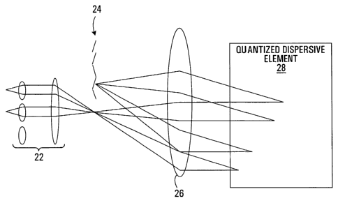
this is shown in Figure 3B. Shown are a number of input ports
coupled through coupling optics 22. Light is coupled through a
main lens 26 to the quantized dispersive element 28 which
causes wavelength dependent dispersion to occur and redirects
light back through the main lens 26 to the array of switching
elements 24. Light then traverses back through the main lens
26 to the quantized dispersive element 28 and back to one of
12
CA 02486740 2004-11-19
WO 03/098961 PCT/CA03/00749
the ports via the coupling optics 22. The quantized dispersive
element 28 has a characteristic such as shown in Figure 3A.
Figure 3C, as for Figure 2B, shows nine beams
containing wavelength spanning three wavelength channels. Due
to the quantized dispersion curve showed in Figure 3A, all~of
the beams within a wavelength band are routed to a respective
single location (thus there are only three locations containing
three overlapped beams shown in the figure). The fill factor no
longer needs to be extremely high, as the overlapped beams are
condensed in the vicinity of the central region of the mirrors.
As long as the switching elements are loosely aligned with.
those overlapped beams, they will be switched efficiently and
with minimal losses. The alignment tolerance can be increased
by providing switching elements slightly bigger than the
overlapped beams. Any relative movement between the switching
array and the dispersive element has no effect as long as the
overlapped beams are still within the boundaries of the
switching element. In the particular case of Figure 3C, a
misalignment to the left has been shown, but has no impact on
the coupling efficiency of the beam. Furthermore, since no
light is impinging on the switching elements' edges, there is
no problem with spurious diffraction.
Figure 3D shows the insertion loss curve for a device
as per an embodiment of the invention and described in Figure
3B when all switching elements axe actuated to couple the light
in the same output port. There is no dip since no light is
lost in the gaps in-between the switching elements.
Therefore, by providing a quantized dispersive
element and an array of switching elements aligned such that
the overlapped beams produced by the quantized dispersive means
lie within the physical boundaries of their respective
13
CA 02486740 2004-11-19
WO 03/098961 PCT/CA03/00749
switching element, a very efficient wavelength switch is
realized that has significantly improved wavelength alignment
tolerance (initial alignment and maintaining of this alignment
over temperature and averse mechanical conditions), no spectral
dips, no spurious diffraction from the switching elements'
edges and lower fill factor requirement for the switching
array.
It should be noted here that since in general
wavelength switches like the one shown in Figure 1 have a flat-
top channel shape, it is counter-intuitive to use a flat-
topping dispersion arrangement within a wavelength switch that
may be one of many reasons why it has never been done before.
It is indeed rather strange to use a complex flat-topping
technology for an intrinsically flat-top device. However this
combination of quantized dispersion and wavelength switching
yields surprising results in terms of optical performances
(mainly absence of dips in-between wavelength channels, absence
of spurious diffraction problem, use of lower fill factor array
of switching elements and improved wavelength alignment
tolerances) .
Figure 4 shows one example of a quantized dispersive
element taught in US patent 6,381,052, V. Delisle hereby
incorporated by reference in its entirety. The arrangement
provides a first dispersion step of D/2 with dispersive element
40, inversion optics 44 for doing an inversion of the
wavelength bands in the focal plane, and providing a second
dispersion amount of D/2 with dispersive element 42 yields a
dispersive device with a staircase-like dispersion curve (see
Figure 8C of the patent cited in reference) useful for
producing flat-top channel shape multiplexors/ demultiplexors.
In the case of Figure 4, transmissive diffraction gratings
14
CA 02486740 2004-11-19
WO 03/098961 PCT/CA03/00749
(shown with a bold dotted line) are used to provide the two
dispersion steps of D/2, while an array of 1:1 micro-telescopes
is used to invert the wavelengths within the predetermined
bands in the focal planes of the second and third lens. The
bands are defined by the physical extent of those micro-lenses
and their spacing.
Another example of a quantized dispersive element is
presented in 6,337,935 by J. Ford hereby incorporated by
reference in its entirety. Again the device is used to produce
a flat top multiplexer. An embodiment of the present
invention contemplates using a pair of such flat top
demultiplexer/multiplexer based on quantized dispersive means
coupled with switching means to perform wavelength switching
with improved performances (mostly enabling the use of low fill
factor switching array).
Figure 5 shows a free-space wavelength switch
embodiment as per the invention, for example based on a
quantized dispersive means as described in U.S. Patent
No. 6,381,052 hereby incorporated by reference in its entirety.
It consists of an array 51 of quantized dispersive elements
50,52,54 (only three shown) and an array S5 of switching
elements 56,58,60 (only three shown) arranged such that each
wavelength within predetermined wavelength bands are routed by
the quantized dispersive element onto a respective switching
element of the switching array. The switching elements
56,58,60, are capable of routing the light from/to any of the
quantized dispersive elements to/from any of the quantized
dispersive elements 50,52,54. In this embodiment, all provided
dispersive elements are quantized.
CA 02486740 2004-11-19
WO 03/098961 PCT/CA03/00749
Other free-space embodiments of a wavelength switch
as per the invention are provided using quantized dispersive
means as described in 6,337,935.
In another embodiment there only needs to be at least
one quantized dispersive element, while the others are regular
continuous dispersive elements. This would enable a reduction
in the cost and the complexity of the device, while still
providing at Least one high quality optical path (the one going
from and to the at least one quantized dispersive element) and
multiple alternate switching paths of lesser optical quality
(i.e. narrower passband). This is typically acceptable in ROADM
applications, where the express traffic needs to be of superior
quality (extremely flat pass band with no spectral dips) and
the local drop traffic can have a non flat-top channel shape
(and in some cases, where the local drop ports are directly
connected to optical receivers, this extra non flat-top
filtering could even be beneficial).
In the example in Figure 5, each quantized
dispersive element performs the subsequent steps of providing a
first dispersion D/2, inverting wavelengths within the
predetermined wavelength bands, and providing a second
dispersion D/2 as taught in 6,381,052. In the embodiment of
Figure 5, a big lens 62 on the right of the picture is used to
provide a telecentric optical system (with the centre of the
second diffraction gratings substantially lying on the focal
plane of this big lens) which simplifies the routing of the
light beams. Lenses 64 collimate light from optical ports (not
shown) to quantized dispersive elements 50,52,54. Figure 6
shows another quantized dispersive element taught in US patent
6,144,783, from R, E. Epworth hereby incorporated by reference
in its entirety where it is explained how the concatenation of
16
CA 02486740 2004-11-19
WO 03/098961 PCT/CA03/00749
two arrayed waveguide gratings 70,72 (AWG) with proper designs,
and most notably with the free spectral range (FSR) of the
first AWG equalling the channel spacing of the second AWG,
yields such a staircase-like dispersion curve (see Figure 5 in
the cited patent). Again, this reference only covers the use of
a quantized dispersion element to realize flat-top channel
shape multiplexors/ demultiplexors. A similar embodiment can be
found in: C. R. Doerr, European Conference on Optical
Communications, PD F.1.1, Amsterdam, 2001.
Figure 7 shows an array 74 of waveguide-based
quantized dispersive elements (five shown) coupled to a low
fill factor array of switching elements 76 through a
combination of cylindrical lenses 78 to realize an embodiment
of a wavelength switch as per the invention. A similar
1S wavelength switch assembly is described in detail in applicants
co-pending patent applications 60/381,364 filed on May 20, 2003
and <attorney docket 50088-4> which is hereby incorporated by
reference in its entirety. In the embodiment shown in Figure
7, the replacement of the continuous dispersive elements by
quantized dispersive elements enables the above mentioned
benefits of using lower fill factor mirror array, absence of
spectral dips and absence of spurious diffraction problems from
the mirrors' edges and improved wavelength alignment tolerances
to the wavelength switch described in the cited patent
application.
Figure 8 shows another preferred embodiment of the
invention using an array 80 of arrayed waveguide based
quantized dispersive elements (three shown) and a low fill
factor array of switching elements 76 and cylindrical lens
combination 78 as in Figure 7. The quantized dispersive
elements each consist of at least two groups of waveguides,
17
CA 02486740 2004-11-19
WO 03/098961 PCT/CA03/00749
each group containing multiple waveguides having a
predetermined relative phase relationship, and one of the at
least two groups having a larger relative phase offset.
Preferably, the design parameters are chosen such that the
phase offset between the at least two groups of waveguides
correspond to the channel spacing (in the case of 100GHz
spacing, this would mean a physical path offset of about 2065.5
microns), while the relative phase relationship between the
waveguides in each of the at least two groups is chosen to
provide a large FSR and the same channel spacing (in the case
of 100GHz spacing and 8THz FSR, the relative physical path
length difference between each consecutive waveguides is about
25.5 microns) .
Figure 9 shows the displacement of the focal spot
after the big lens of Figure 8 if a continuous dispersive
element is used as disclosed in applicants invention as claimed
in the above referenced co-pending patent applications . In
this specific example, 250 waveguides have been used, with a
relative path length difference of 25.5 microns. The big lens's
focal length has been arbitrarily chosen to be 5 mm, but the
actual value depends mainly on the limitation of the mirror
array tilting angle and the smallest mirror array pitch
achievable. As is clearly shown on Figure 9, the peak of the
focussed spots is displaced continuously with frequency over
the -30 GHz to +30 GHz range with respect to ITU.
Figure 10 shows a similar plot as in Figure 9
corresponding to the preferred embodiment described in Figure
8, with each quantized dispersion element containing 2 groups
of 125 waveguides having a physical path length offset of
2065.5 microns between each group and each of the 125
waveguides in a group having a relative optical path length
18
CA 02486740 2004-11-19
WO 03/098961 PCT/CA03/00749
difference of 25.5 microns. As can be seen on the figure, the
peaks of the light beams do not substantially move over a range
of -30 GHz to +30 GHz with respect to ITU. This corresponds to
a quantized dispersion operation since all the beams carrying
the wavelength within this -30 GHz to 30 GHz wavelength band
are all routed to the same position. The side lobe level is a
little high with these specific parameters, but could be
reduced by design optimization.
Figure 11 shows the same result as shown in Figure 10
but over a broader frequency range. The quantized operation of
the quantized dispersive element is clearly Shown in that only
a finite set of locations are possible for the focussed light
beams, corresponding to a channel spacing of 100 GHz (in the
case of the figure, there are only 3 locations permitted
corresponding to -100, 0 and +100 GHz).
Figure 12 shows another embodiment as per the
invention in which the switching elements are transmissive
switching elements 100. Although the figure shows a similar
embodiment to that of Figure 7, the transmissive arrangement
can be used with any alternate combination of dispersive means,
waveguide or free-space optics based. The transmissive
switching. elements 100 are capable of routing the light beam
going through them from an input quantized dispersion element
102 at the left of the Figure to any of the output dispersion
elements 120 on the right of the Figure. At least one of the
output dispersive elements 120 is a quantized dispersion
element to provide at least one high quality optical port (with
wide flat-top passband and no spectral dips), although the
figure is shown with all 5 output dispersive elements being
quantized. The array of transmissive switching elements 100 can
be fabricated using electro-holograms, optical phase arrays,
19
CA 02486740 2004-11-19
WO 03/098961 PCT/CA03/00749
liquid Crystal beam steering elements, movable micro-prisms or
movable micro-lenses. Full details of this embodiment, but
with continuous dispersive elements, are provided in applicants
co-pending patent applications 60/381,364 filed on May 20, 2003
and <attorney docket 50088-4> which is hereby incorporated by
reference in its entirety. The invention described in this
document basically enables to dissociate the design of the
optical filtering response (mainly governed by the quantized
dispersive element) from the design of the space switch itself.
This is particularly important for the case of a wavelength
cross-connect, since the switching requirements (larger beams
are easier to switch) contradicts the wavelength filtering
requirements (smaller beams are preferred to increase the
spectrograph resolution, thus the channel shape). Typically,
this difference is quite pronounced, usually a factor of two or
more. With the described invention, it is possible to use
whatever beam size is convenient for the switching core and
design the necessary optics, while the wavelength filtering
response is still primarily governed by how efficiently a
quantized dispersion profile has been obtained.
It is also possible using the teachings of the
present invention to use quantized dispersive means and an
array of light processing means (capable of attenuating power,
changing polarization state or detecting light signals,
performing a limiting function) with the same benefit of
enabling the use of a low fill factor array of light processing
means.
CA 02486740 2004-11-19
WO 03/098961 PCT/CA03/00749
Numerous modifications and variations of the present
invention are possible in light of the above teachings. It is
therefore to be understood that within the sCOpe of the
appended claims, the invention may be practised otherwise than
as specifically described herein.
21