Note: Descriptions are shown in the official language in which they were submitted.
CA 02487602 2007-11-08
METAL AND CERAMIC BLEND DONOR ROLL COATINGS
BACKGROUND
The present invention relates to coatings for members of
ionographic or electrophotographic machines, including digital, image on
image, imaging, copying, and printing apparatuses and machines. In
embodiments, the present invention is directed to coatings for donor
members. In embodiments, the invention is directed to coatings for donor
members including donor rollers and the like, and electrodes closely
spaced from a donor member to form a toner powder cloud in a
development zone to develop a latent image. The present invention is
directed, in embodiments, to suitable conductive and semiconductive
overcoatings, especially for donor member or transport members like
scavengeless or hybrid scavengeless development systems. In
embodiments, the coatings include a blend of metal and ceramic.
Generally, the process of electrophotographic printing includes
charging a photoconductive member to a substantially uniform potential so
as to sensitize the surface thereof. The charged portion of the
photoconductive surface is exposed to a light image of an original
document being reproduced. This records an electrostatic latent image on
the photoconductive surface. After the electrostatic latent image is
recorded on the photoconductive surface, the latent image is developed.
Two component and single component developer materials are commonly
used for development. The following discusses the development process.
Toner particles are attracted to the latent image forming a toner powder
image on the photoconductive surface. The toner image is subsequently
transferred to a copy sheet. Finally, the toner powder image is heated to
permanently fuse it to the copy sheet in image configuration.
-1-
CA 02487602 2007-11-08
One type of development system is a single component
development system such as a scavengeless development system that
uses a donor roll for transporting charged toner (single component
developer) to the development zone. At least one, and preferably a
plurality of electrode members, are closely spaced to the donor member in
the development zone. An AC voltage is applied to the electrode members
forming a toner cloud in the development zone. The electrostatic fields
generated by the latent image attract toner from the toner cloud to develop
the latent image.
Another type of development system is a two component
development system such as a hybrid scavengeless development system
which employs a magnetic brush developer member for transporting carrier
having toner (two component developer) adhering triboelectrically thereto.
A donor member is used in this configuration also to transport charged
toner to the development zone. The donor member and magnetic member
are electrically biased relative to one another. Toner is attracted to the
donor member from the magnetic member. The electrically biased
electrode members detach the toner from the donor member forming a
toner powder cloud in the development zone, and the latent image attracts
the toner particles thereto. In this way, the latent image recorded on the
photoconductive member is developed with toner particles.
Coatings for donor members are known and may contain a
dispersion of conductive particles in a dielectric binder. The desired
volume resistivity is achieved by controlling the loading of the conductive
material. However, very small changes in the loading of conductive
materials at or near the percolation threshold can cause dramatic changes
in resistivity. Furthermore, changes in the particle size and shape of such
materials can cause wide variations in the resistivity at constant weight
loading. If the resistivity is too low, electrical breakdown of the coating
can
occur when a voltage is applied to an electrode or material in contact with
the coating. Also, resistive heating can cause the formation of holes in the
-2-
CA 02487602 2007-11-08
coating. When the resistivity is too high, charge accumulation on the
surface of the overcoating can create a voltage which changes the
electrostatic forces acting on the toner. The problem of the sensitivity of
the resistivity to the loading of conductive materials in an insulative
dielectric binder is avoided, or minimized with the coatings of the present
invention.
Currently, ceramic materials are used for donor members such as
donor members used in hybrid scavengeless development apparatuses
and hybrid jumping development (HJD). Several problems may be
associated with the use of ceramic materials inciuding non-uniform
thickness, non-uniform run-out, pinhole defects, and rough surface finish.
These problems can result in print defects. The problems are not easily
overcome because they may be related to the deformation of substrate
during high temperature thermal spray coating of ceramic materials.
Grinding the ceramic coatings is needed to provide the desired surface
finish.
However, with the coatings of the present invention, the above
problems with use of ceramic materials are reduced or eliminated.
U.S. Patent 5,600,414 discloses a charging roller with blended
ceramic layer. The ceramic layer includes plasma spraying of a blend of
insulating ceramic material and a semiconductive ceramic material in a
specified ratio. The desired blend is alumina and titania.
U.S. Patent 6,560,432 BI discloses a donor roll having a ceramic
outer layer coating. The coating consists of particles containing a ratio of
pure alumina and pure titania held together with an organic binder.
There exists a need for a donor member coating which provides
conductivity or resistivity within a desired range, minimizes residue voltage,
is relatively uniform and virtually free from defects and pinholes, provides
good wear resistance for up to several million copies and/or prints, for
example 10 million copies or prints, provides consistent performance with
-3-
CA 02487602 2007-11-08
variable temperature and humidity, is low in manufacturing cost, and is
environmentally acceptable. In addition, there exists a need for wear
resistant, electrically tunable coatings for hybrid scavengeless and hybrid
jumping development.
SUMMARY
Embodiments of the present invention include: a donor member
comprising a substrate and thereover a coating comprising ceramic and
metal.
Embodiments further include: an apparatus for developing a latent
image recorded on a surface, comprising: a) wire supports; b) a donor
member spaced from the surface and being adapted to transport toner to a
region opposed from the surface, wherein said donor member comprises a
substrate and thereover a coating comprising ceramic and metal; and c) an
electrode member positioned in the space between the surface and said
donor member, said electrode member being closely spaced from said
donor member and being electrically biased to detach toner from said
donor member thereby enabling the formation of a toner cloud in the space
between said electrode member and the surface with detached toner from
the toner cloud developing the latent image.
Moreover, embodiments include: an image forming apparatus for
forming images on a recording medium comprising a) a charge-retentive
surface to receive an electrostatic latent image thereon; b) a development
component to apply toner to said charge-retentive surface to develop said
electrostatic latent image to form a developed image on said charge
retentive surface, said development component comprising a donor
member comprising a substrate and thereover a coating comprising
ceramic and metal; and c) a transfer component to transfer the developed
image from said charge retentive surface to a copy substrate.
-4-
CA 02487602 2007-11-08
According to another aspect of the present invention, there is
provided a donor member comprising a substrate and thereover a coating
comprising ceramic and metal, wherein said ceramic is present in said
coating in an amount of from about 80 to about 99 percent by weight of
total solids.
According to another aspect of the present invention, there is
provided an apparatus for developing a latent image recorded on a surface,
comprising:
a) a donor member spaced from the surface and being adapted
to transport toner to a region opposed from the surface, wherein said donor
member comprises a substrate and thereover a coating comprising ceramic
and metal, wherein said ceramic is present in said coating in an amount of
from about 80 to about 99 percent by weight of total solids; and
b) an electrode member positioned in the space between the
surface and said donor member, said electrode member being closely
spaced from said donor member and being electrically biased to detach
toner from said donor member thereby enabling the formation of a toner
cloud in the space between said electrode member and the surface with
detached toner from the toner cloud developing the latent image.
According to a further aspect of the present invention, there is
provided an image forming apparatus for forming images on a recording
medium comprising:
a) a charge-retentive surface to receive an electrostatic latent
image thereon;
b) a development component to apply toner to said charge-
retentive surface to develop said electrostatic latent image to form a
developed image on said charge retentive surface, said development
component comprising a donor member comprising a substrate and
thereover a coating comprising ceramic and metal, wherein said ceramic is
present in said coating in an amount of from about 80 to about 99 percent
by weight of total solids; and
-5-
CA 02487602 2007-11-08
c) a transfer component to transfer the developed image from
said charge retentive surface to a copy substrate.
BRIEF DESCRIPTION OF THE DRAWINGS
For a better understanding of the present invention, reference may
be had to the accompanying figures.
Figure 1 is a schematic illustration of an image apparatus in
accordance with the present invention.
Figure 2 is a schematic illustration of an embodiment of a
development apparatus useful in an electrophotographic printing machine.
Figure 3 is an enlarged illustration of a donor roll.
DETAILED DESCRIPTION
The present invention relates to coatings for donor members in
development units for electrostatographic, including digital, image on
image, imaging and printing apparatuses, and especially for hybrid
scavengeless development and hybrid jumping development units.
Referring to Figure 1, in a typical electrostatographic reproducing
apparatus, a light image of an original to be copied is recorded in the form
of an electrostatic latent image upon a photosensitive member and the
latent image is subsequently rendered visible by the application of
electroscopic thermoplastic resin particles which are commonly referred to
as toner. Specifically, photoreceptor 10 is charged on its surface by means
of a charger 12 to which a voltage has been supplied from power supply
11. The photoreceptor 10 is then imagewise exposed to light from an
optical system or an image input apparatus 13, such as a laser and light
emitting diode, to form an electrostatic latent image thereon. Generally, the
electrostatic latent image is developed by bringing a developer mixture
from developer station 14 into contact therewith. Shown in Figure 1 is
-6-
CA 02487602 2007-11-08
donor roller 40. Development can be affected by use of a magnetic brush,
powder cloud, or other known development process. A dry developer
mixture usually comprises carrier granules having toner particles adhering
triboelectrically thereto. Toner particles are attracted from the carrier
granules to the latent image forming a toner powder image thereon.
Alternatively, a liquid developer material may be employed, which includes
a liquid carrier having toner particles dispersed therein.
After the toner particles have been deposited on the
photoconductive surface, in image configuration, they are transferred to a
copy sheet 16 by transfer means 15, which can be pressure transfer or
electrostatic transfer. Alternatively, the developed image can be
transferred to an intermediate transfer member, or bias transfer member,
and subsequently transferred to a copy sheet. Examples of copy substrates
include paper, transparency material such as polyester, polycarbonate, or
the like, cloth, wood, or any other desired material upon which the finished
image will be situated.
After the transfer of the developed image is completed, copy sheet
16 advances to fusing station 19, depicted in Figure 1 as fuser roll 20 and
pressure roll 21 (although any other fusing components such as fuser belt
in contact with a pressure roll, fuser roll in contact with pressure belt, and
the like, are suitable for use with the present apparatus), wherein the
developed image is fused to copy sheet 16 by passing copy sheet 16
between the fusing and pressure members, thereby forming a permanent
image. Alternatively, transfer and fusing can be effected by a transfix
application.
Photoreceptor 10, subsequent to transfer, advances to cleaning
station 17, wherein any toner left on photoreceptor 10 is cleaned therefrom
by use of a blade 1(as shown in Figure 1), brush, or other cleaning
apparatus.
-7-
CA 02487602 2007-11-08
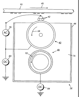
Referring now to Figure 2, in an embodiment of the invention,
developer unit 14 develops the latent image recorded on the
photoconductive surface of photoreceptor 10. Preferably, developer unit 14
includes donor roller 40 and electrode member or members 42. Electrode
members 42 are electrically biased relative to donor roll 40 to detach toner
therefrom so as to form a toner powder cloud in the gap between the donor
roll 40 and photoconductive surface of photoreceptor 10. The latent image
attracts toner particles from the toner powder cloud forming a toner powder
image thereon. Donor roller 40 is mounted, at least partially, in the
chamber 76 of developer housing 44. The chamber 76 in developer
housing 44 stores a supply of developer material which is a two component
developer material of at least carrier granules having toner particles
adhering triboelectrically thereto. A magnetic roller 46 disposed interior of
the chamber 76 of housing 44 conveys the developer material to the donor
roller 40. The magnetic roller 46 is electrically biased relative to the donor
roller 40 so that the toner particles are attracted from the magnetic roller
46
to the donor roller 40.
The donor roller 40 can be rotated in either the 'with' or 'against'
direction relative to the direction of motion of photoreceptor 10. In Figure
2,
donor roller 40 is shown rotating in the direction of arrow 68. Similarly, the
magnetic roller 46 can be rotated in either the 'with' or 'against' direction
relative to the direction of motion of photoreceptor 10. In Figure 2,
magnetic roller 46 is shown rotating in the direction of arrow 92.
Photoreceptor 10 moves in the direction of arrow 45.
A pair of electrode members 42 are shown extending in a direction
substantially parallel to the longitudinal axis of the donor roller 40. The
electrode members 42 are made from one or more thin (i.e., 50 to 100 m
in diameter) stainless steel or tungsten electrode members 42 which are
closely spaced from donor roller 40. The distance between the electrode
members and the donor roller 40 is from about 5 to about 35 m, or about
10 to about 25 m or the thickness of the toner layer on the donor roll. The
-8-
CA 02487602 2007-11-08
electrode members 42 are self-spaced from the donor roller 40 by the
thickness of the toner on the donor roller 40.
As illustrated in Figure 2, an alternating electrical bias is applied to
the electrode members 42 by an AC voltage source 78. The applied AC
establishes an alternating electrostatic field between the electrode
members 42 and the donor roller 40 is effective in detaching toner from the
donor roller 40 and forming a toner cloud about the electrode members 42,
the height of the cloud being such as not to be substantially in contact with
the photoreceptor 10. The magnitude of the AC voltage is relatively low
and is in the order of 200 to 500 volts peak at a frequency ranging from
about 9 kHz to about 15 kHz. A DC bias supply 80 which applies
approximately 300 volts to donor roller 40 establishes an electrostatic field
between photoreceptor 10 and donor roller 40 for attracting the detached
toner particles from the cloud surrounding the electrode members 42 to the
latent image recorded on the photoconductive member. At a spacing
ranging from about 10 m to about 40 m between the electrode members
42 and donor roller 40, an applied voltage of 200 to 500 volts produces a
relatively large electrostatic field without risk of air breakdown. A DC bias
supply 84 which applies approximately 100 volts to magnetic roller 46
establishes an electrostatic field between magnetic roller 46 and donor
roller 40 so that an electrostatic field is established between the donor
roller
40 and the magnetic roller 46 which causes toner particles to be attracted
from.
In an alternative embodiment of the present invention, one
component developer material consisting of toner without carrier may be
used. In this configuration, the magnetic roller 46 is not present in the
developer housing 44. This embodiment is described in more detail in U.S.
Patent 4,868,600.
The donor member of the present invention may be in the form of a
donor roller 40 as depicted in Figure 2 and 3, or in another known
configuration. As shown in Figure 3, the donor member 40 includes a
-9-
CA 02487602 2007-11-08
substrate 41 which may comprise metal substrates such as, for example,
copper, aluminum, nickel, and the like metals, plastics such as, for
example, polyesters, polyimides, polyamides, and the like, glass and like
substrates, which may be optionally coated with thin metal films, and a
coating 43 including a blend of ceramic and metal.
Examples of suitable ceramics include alumina including, for
example, pure alumina, chromium oxide, silicon nitride, silicone carbide,
zirconium, and the like ceramics, and mixtures thereof.
Examples of suitable metals include molybdenum, tungsten,
tantalum, and the like metals, and mixtures thereof.
The metal is present in the outer blended coating in an amount of
from about 1 to about 20 weight percent with respect to the total weight of
metal and other solids in the outer layer, or from about 10 to about 12
weight percent by weight of total solids. The ceramic is present in the outer
blended coating in an amount of from about 80 to about 99 percent by
weight of total soiids, or from about 90 to about 92 percent by weight of
total solids.
In an embodiment, the outer donor member layer 43 comprises a
blend of molybdenum and alumina.
ln embodiments, the outer donor member coating 43 has a resistivity
of from about 103 to about 1010, or from about 106 to about 109 ohms-cm, or
about 108 ohms-cm.
The blended outer coatings herein are formed by known methods
including alumina powder and molybdenum powder provided by Saint
Gobain of Northhampton, Massachusetts. These materials can be blended
to the appropriate weight percent using a standard v-blender. The blended
powder may then be coated onto a donor member using known methods
such as spraying, dipping, roll coating, flow coating, extrusion, and the
like.
In embodiments, the outer layer is plasma spray coated onto a donor
member substrate, or over a coating on a donor member substrate.
-10-
CA 02487602 2007-11-08
The blended outer coating on the donor member substrate is coated
to a thickness of from about 200 to about 400 microns, or from about 250 to
about 300 microns.
In an embodiment of the invention, an additional outer protective
coating may be present on the blended layer coating described above. The
outer protective layer may comprise inorganic or organic materials with
coating thicknesses in the range of from about 10 nm to about 10 micron,
or from about 0.5 to about 5 micron. The inorganic coatings may comprise
polysilicates derived from a sol-gel process and diamond-like
nanocomposites derived from plasma deposition, and mixtures thereof.
The organic coatings may comprise soluble polymers or cross-linked
polymers. Soluble polymers include but not limited to polycarbonates,
polyimides, polyamides, polyesters, polysiloxanes, polyesters and mixtures
thereof. Crosslinked polymers can be selected from but not limited to
thermal or radiation curable vinyl or epoxy monomers, oligomers and
polymers, unsaturated polyesters, polyamides, carbazole containing
polymers, thiophene containing polymers, bistriarylamine containing
polymers, and mixtures thereof. The organic coatings may contain
additives in the range of from about 0.1 to about 50 percent by weight of
the protective coatings. The additives include, but are not limited to,
charge transport molecules and oxidants, the oxidized charge transport
molecule salts, and particulate fillers such as silica,
polytetrafluoroethylene
or TEFLON powder, carbon fibers, carbon black, and mixtures thereof. In
embodiments, an outer protective coating may not be used.
The blended coating may be coated onto a donor member including
a donor roller, belt, or applied over electrode donor members such as
electrode wires. The outer coating may be ground using a diamond wheel
to a desired surface finish and thickness.
The following Examples further define and describe embodiments of
the present invention. Unless otherwise indicated, all parts and
percentages are by weight.
-11-
CA 02487602 2007-11-08
EXAMPLES
Example 1
Preparation of Roller Substrate
A suitable roller substrate or core can be gritblasted to a suitable
surface finish.
Example 2
Preparation of Bond Coat
It is possible to use a bond coat to enhance adhesion of the coating
to the roller or sleeve. A chrome aluminum yttrium cobalt powder,
commercially available from Praxair as CO-106-1, can be plasma sprayed
over a grit blasted steel substrate according to manufacturer recommended
spray parameters accompanying the powder. This would be followed by an
optional plasma spray midcoat consisting of a 1:1 by volume mixture of
chrome aluminum yttrium cobalt powder and titanium dioxide commercially
available from Sulzer Metco as 102. Other commercially available bond
coats are believed to be useful for either or both bond or mid-coating.
Example 3
Blended Ceramic/Metal Coating
Plasma spray coating of a blended alumina/molybdenum layer was
accomplished with Praxair Thermal Spray Equipment using a SG 100
torch. The powder was obtained from Saint Gobain of Northhampton,
Massachusetts, and mechanically blended to specific weight ratios. The
coating was sprayed to between 250 and 400 microns thickness.
Alternative plasma coating approaches can use other equipment, gases,
and/or powder particle sizes, wherein parameters are adjusted accordingly
to achieve the same or similar result. For example, High Velocity Oxy Fuel
(HVOF) or other thermal spray processes are believed to be adaptable and
satisfactory to achieving comparable and equivalent coating results.
-12-
CA 02487602 2007-11-08
Example 4
Grinding of Blended Alumina/Molybdenum Outer Coating
The coating can be ground to between 150 and 200 microns
thickness to achieve a desired diameter and surface finish.
While the invention has been described in detail with reference to
specific and preferred embodiments, it will be appreciated that various
modifications and variations will be apparent to the artisan. All such
modifications and embodiments as may readily occur to one skilled in the
art are intended to be within the scope of the appended claims
-13-